EP2793400B1 - Commutateurs de permutation double pour répondre aux demandes de linéarité d'agrégation de porteuses - Google Patents
Commutateurs de permutation double pour répondre aux demandes de linéarité d'agrégation de porteuses Download PDFInfo
- Publication number
- EP2793400B1 EP2793400B1 EP14169092.5A EP14169092A EP2793400B1 EP 2793400 B1 EP2793400 B1 EP 2793400B1 EP 14169092 A EP14169092 A EP 14169092A EP 2793400 B1 EP2793400 B1 EP 2793400B1
- Authority
- EP
- European Patent Office
- Prior art keywords
- switch
- antenna
- band
- low
- signal
- Prior art date
- Legal status (The legal status is an assumption and is not a legal conclusion. Google has not performed a legal analysis and makes no representation as to the accuracy of the status listed.)
- Not-in-force
Links
- 230000002776 aggregation Effects 0.000 title claims description 10
- 238000004220 aggregation Methods 0.000 title claims description 10
- 230000009977 dual effect Effects 0.000 title description 19
- 238000000034 method Methods 0.000 claims description 17
- 230000008569 process Effects 0.000 claims description 9
- 230000004044 response Effects 0.000 claims description 9
- 238000010295 mobile communication Methods 0.000 claims description 8
- ZCJJIQHVZCFSGZ-UHFFFAOYSA-N 2,8-bis(diphenylphosphoryl)dibenzothiophene Chemical compound C=1C=CC=CC=1P(C=1C=C2C3=CC(=CC=C3SC2=CC=1)P(=O)(C=1C=CC=CC=1)C=1C=CC=CC=1)(=O)C1=CC=CC=C1 ZCJJIQHVZCFSGZ-UHFFFAOYSA-N 0.000 description 61
- 238000004891 communication Methods 0.000 description 28
- 230000001413 cellular effect Effects 0.000 description 10
- 238000010586 diagram Methods 0.000 description 9
- 230000005540 biological transmission Effects 0.000 description 8
- 230000015654 memory Effects 0.000 description 7
- 238000005516 engineering process Methods 0.000 description 6
- 230000006870 function Effects 0.000 description 4
- 238000012545 processing Methods 0.000 description 3
- 230000010267 cellular communication Effects 0.000 description 2
- 230000000694 effects Effects 0.000 description 2
- 230000007774 longterm Effects 0.000 description 2
- 238000005259 measurement Methods 0.000 description 2
- 238000012986 modification Methods 0.000 description 2
- 230000004048 modification Effects 0.000 description 2
- 238000010521 absorption reaction Methods 0.000 description 1
- 238000003491 array Methods 0.000 description 1
- 230000008901 benefit Effects 0.000 description 1
- 229910010293 ceramic material Inorganic materials 0.000 description 1
- 238000004590 computer program Methods 0.000 description 1
- 238000010276 construction Methods 0.000 description 1
- 230000003247 decreasing effect Effects 0.000 description 1
- 230000001419 dependent effect Effects 0.000 description 1
- 239000003989 dielectric material Substances 0.000 description 1
- 238000005562 fading Methods 0.000 description 1
- 238000001914 filtration Methods 0.000 description 1
- 239000012774 insulation material Substances 0.000 description 1
- 238000001465 metallisation Methods 0.000 description 1
- 230000005404 monopole Effects 0.000 description 1
- 238000006386 neutralization reaction Methods 0.000 description 1
- 238000000059 patterning Methods 0.000 description 1
- 230000002441 reversible effect Effects 0.000 description 1
- 238000012552 review Methods 0.000 description 1
- 230000003595 spectral effect Effects 0.000 description 1
- 239000000758 substrate Substances 0.000 description 1
Images



Classifications
-
- H—ELECTRICITY
- H04—ELECTRIC COMMUNICATION TECHNIQUE
- H04B—TRANSMISSION
- H04B1/00—Details of transmission systems, not covered by a single one of groups H04B3/00 - H04B13/00; Details of transmission systems not characterised by the medium used for transmission
- H04B1/005—Details of transmission systems, not covered by a single one of groups H04B3/00 - H04B13/00; Details of transmission systems not characterised by the medium used for transmission adapting radio receivers, transmitters andtransceivers for operation on two or more bands, i.e. frequency ranges
Definitions
- the present inventive concepts generally relate to the field of communications and, more particularly, to antennas and wireless electronic devices incorporating the same.
- GSM global system for mobile communications
- DCS digital cellular system
- UMTS Universal Mobile Telecommunications System
- GSM global system for mobile communications
- DCS digital cellular system
- UMTS Universal Mobile Telecommunications System
- TRP total radiated power
- FEM platform front-end-module
- Wireless communication devices such as WIFI 802.11N and LTE compliant communication devices, are increasingly using Multiple Input-Multiple Output (MIMO) antenna technology to provide increased data communication rates with decreased error rates.
- MIMO antenna includes at least two antenna elements.
- MIMO technology may offer significant increases in data throughput and/or transmission range without the need for additional bandwidth or transmit power. It can achieve this due to the ability of MIMO to obtain higher spectral efficiency (more bits per second per hertz of bandwidth) and/or reduced fading.
- MIMO based systems allow the use of a variety of coding techniques that take advantage of the presence of multiple transmit and receive antennas.
- wireless communications performed over a MIMO channel can use beamforming, spatial multiplexing and/or diversity coding techniques.
- CA downlink carrier aggregation
- main + diversity two receivers, two at each frequency band (main + diversity) are working at the same time but with only one transmitter.
- DPDT antenna swapping switch
- Document WO2012/048741 discloses an antenna switch structure comprising a plurality of transceivers, a low frequency band antenna and a high frequency band antenna.
- the antenna switch structure also comprises a first receiver comprising a low band diversity circuit path configured to process signals of a low diversity frequency band and a second receiver comprising a high band diversity circuit path configured to process signals of a high diversity frequency band.
- the structure also comprises first and second low band antennas configured to transmit and receive wireless signals of a low frequency band and first and second high band antennas configured to transmit and receive wireless signals of a high frequency band.
- the structure further comprises a first low pass filter connected to the first low band antenna and a second low pass filter connected to the second low band antenna.
- the structure also comprises a first switch and a second switch.
- the first switch is controlled to switch between a first mode that connects the first low pass filter to the first transceiver and the second low pass filter to the first receiver and a second mode that connects the first low pass filter to the first receiver and the second low pass filter to the first transceiver.
- the mode of the first switch is selected in response to signals received at the first switch.
- the second switch is controlled to switch between a first mode that connects the first high band antenna to the second transceiver and the second high band antenna to the second receiver and a second mode that connects the first high band antenna to the second receiver and the second high band antenna to the second transceiver.
- the mode of the second switch is selected in response to signals received at the second switch.
- the mode of the first switch is further selected in response to a frequency of a signal received at the second switch and the mode of the second switch is further selected in response to a frequency of a signal received at the first switch.
- the first mode of the first switch transmits a low band main signal to the low band main circuit path of the first transceiver and the second mode of the first switch transmits a low band diversity signal to the low band diversity circuit path of the first receiver.
- the first mode of the second switch transmits a high band main signal to the high band main circuit path of the second transceiver and the second mode of the second switch transmits a high band diversity signal to the high band diversity circuit path of the second receiver.
- the first switch is configured to switch between transmitting a signal to the first low pass filter and transmitting a signal to the second low pass filter
- the second switch is configured to switch between transmitting a signal to the first high band antenna and transmitting a signal to the second high band antenna.
- the antenna switch structure may perform carrier aggregation.
- spatially relative terms such as “above”, “below”, “upper”, “lower” and the like, may be used herein for ease of description to describe one element or feature's relationship to another element(s) or feature(s) as illustrated in the figures. It will be understood that the spatially relative terms are intended to encompass different orientations of the device in use or operation in addition to the orientation depicted in the figures. For example, if the device in the figures is turned over, elements described as “below” other elements or features would then be oriented “above” the other elements or features. Thus, the exemplary term “below” can encompass both an orientation of above and below. The device may be otherwise oriented (rotated 90 degrees or at other orientations) and the spatially relative descriptors used herein interpreted accordingly. Well-known functions or constructions may not be described in detail for brevity and/or clarity.
- wireless electronic devices may include multi-band wireless communication terminals (e.g., portable electronic devices/wireless terminals/mobile terminals/terminals) that are configured to carry out cellular communications (e.g., cellular voice and/or data communications) in more than one frequency band.
- cellular communications e.g., cellular voice and/or data communications
- present inventive concepts are not limited to such embodiments and may be embodied generally in any device and/or system that is configured to transmit and receive in two or more frequency bands.
- mobile communication terminal includes, but is not limited to, a terminal that is configured to receive and/or transmit communication signals via a wireless air interface with, for example, a cellular network, a wireless local area network (WLAN), and/or another communication terminal (e.g., via a Bluetooth interface).
- mobile communication terminals include, but are not limited to, cellular phones, satellite phones, headsets (e.g., Bluetooth headset), laptop and/or palmtop computers configured to receive and/or transmit wireless communication signals.
- embodiments of the invention may be implemented in an electronic device, such as a mobile terminal, that includes a Multiple-Input Multiple-Output (MIMO) antenna that is configured to transmit and receive RF signals in two or more frequency bands.
- MIMO antenna may be configured, for example, to transmit/receive RF communication signals in the frequency ranges used for cellular communications (e.g., cellular voice and/or data communications), WLAN communications, and/or TransferJet communications, etc.
- the term "mobile terminal” may include a satellite or cellular radiotelephone with or without a multi-line display; a Personal Communications System (PCS) terminal that may combine a cellular radiotelephone with data processing, facsimile and data communications capabilities; a PDA or smart phone that can include a radiotelephone, pager, Internet/intranet access, Web browser, organizer, calendar and/or a global positioning system (GPS) receiver; and a conventional laptop and/or palmtop receiver or other appliance that includes a radiotelephone transceiver.
- Mobile terminals may also be referred to as "pervasive computing" devices.
- the network may provide services broadly labeled as PCS (Personal Communications Services) including advanced digital cellular systems conforming to standards such as IS-136 and IS-95, lower-power systems such as DECT (Digital Enhanced Cordless Telephone), data communications services such as CDPD (Cellular Digital Packet Data), and other systems such as CDMA-2000, that are proposed using a format commonly referred to as Wideband Code Division Multiple Access (WCDMA).
- PCS Personal Communications Services
- advanced digital cellular systems conforming to standards such as IS-136 and IS-95
- DECT Digital Enhanced Cordless Telephone
- CDPD Cellular Digital Packet Data
- CDMA-2000 Wideband Code Division Multiple Access
- LTE mobile devices may need antenna systems that cover twenty or more frequency bands, including, but not limited to, 704-746MHz, 760-800 MHz, 824-894 MHz, 880-960 MHz, 1710-1850 MHz, 1820- 1990 MHz, 1920-2170 MHz, and 2500-2700 MHz.
- the antenna systems used in LTE devices may also need to meet the requirements of Single In-Single Output (SISO) and Single In-Multiple Output (SIMO) applications for other 3GPP and 2G bands.
- SISO Single In-Single Output
- SIMO Single In-Multiple Output
- the antenna systems may be required to meet Specific Absorption Rate (SAR) requirements and other industry standards.
- an intelligent control system may be used to select particular antenna(s) for transmitting and receiving wireless signals based on various performance factors and criteria.
- the antenna selection may be based on various modes of operation of the device, such as particular ways a user holds the device during operation.
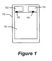
- Figure 1 illustrates a mobile terminal 100 including a MIMO antenna that includes at least two radiating elements or antennas 152, 154.
- the first and second radiating elements 152, 154 may be formed on a planar substrate, such as on a conventional printed circuit board, which includes a dielectric material, ceramic material, or insulation material.
- the first and second radiating elements 152, 154 are adjacent to grounding elements 160, which couple the first and second radiating elements 152, 154 to a ground plane on the printed circuit board.
- the first and second radiating elements 152, 154 may be formed by patterning a conductive (e.g., metallization) layer on a printed circuit board.
- the ground plane 160 may act as a counterpoise for each of the first and second radiating elements 152, 154.
- RF signals are coupled to the first radiating element 152 through a first feed element or port 162, while RF signals are coupled to the second radiating element 154 through a second feed element or port 164.
- the first feed element 162 is coupled to the first radiating element 152 near an end of the first radiating element 152, so that the first radiating element 152 generally extends away from the first feed element 162 along an upper end of the mobile terminal 100.
- the second feed element 164 is coupled to the second radiating element 154 near an end of the second radiating element 154, so that the second radiating element 152 generally extends away from the second feed element 164 along the upper end of the mobile terminal 100.
- the two radiating elements 152 and 154 may be separated via an isolator element.
- the radiating elements or antennas 152, 154 may be disposed in a variety of positions in mobile terminal 100 in accordance with various embodiments of the present invention. Moreover, more than two antennas can be used in other embodiments of the present invention.
- FIG. 2 is a block diagram illustrating an example MIMO antenna system 200 for selecting an antenna in a mobile terminal, such as mobile terminal 100 of Figure 1 .
- the MIMO antenna system 200 comprises antennas 250 and 260, comparable to radiating elements 152 and 154 of Figure 1 , which are connected to downconvertor circuitry via a DPDT 240.
- the downconvertor circuitry comprises low noise amplifiers (LNAs) 224 and 232 in the main circuit path 220 and diversity circuit path 230, respectively, along with power amplifiers (PAs) 222 in the main circuit path.
- LNAs low noise amplifiers
- PAs power amplifiers
- a Radio Frequency (RF) Application Specific Integrated Circuit (ASIC) 210 is coupled to the amplifier circuits 222, 224 and 232 and may be configured to implement the mixer circuits, oscillators, and input/output filters to generate the complex baseband signal from a received RF signal via antennas 250 and 260 and to generate the RF signal for transmission on one of the antennas 250 and 260 from a complex baseband signal.
- RF Radio Frequency
- ASIC Application Specific Integrated Circuit
- the DPDT 240 is operable in response to various control circuitry and signals to select one the antennas 250 and 260 for transmission and to select which of the antennas 250 and 260 is to be used for the main circuit path signal and which is to be used for the diversity circuit path signal when processing a received RF signal.
- Carrier aggregation is a technique where two or more frequency bands are used together in order to increase the total (aggregated) bandwidth.
- CA Carrier aggregation
- a harmonic of the transmitted signal falls directly in the receive band of the other carrier, there will be extremely high linearity requirements on the circuit path between the transmitter and the antenna.
- the harmonic of a transmission frequency of 700MHz may be three times as high, equivalent to the 2100 MHz receiving frequency.
- extreme linearity requirements will be put on the antenna swapping switch (DPDT) when the antenna swapping technique is combined with CA.
- DPDT antenna swapping switch
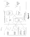
- FIG. 3 is a block diagram illustrating MIMO antenna system 300 for selecting antennas in a mobile terminal according to some embodiments.
- the MIMO antenna system 300 is similar to that illustrated in FIG. 2 , but includes dual swapping switch system 320.
- Dual swapping switch system 320 includes two or more DPDT switches, such as DPDT 1 330 and DPDT 2 340.
- System 320 also includes diplexer 1 350 and diplexer 2 360.
- DPDT 1 330 is connected to diplexer 1 350 and/or diplexer 2 360.
- DPDT 2 340 is connected to diplexer 1 350 and/or diplexer 2 360.
- Diplexer 1 350 is electrically connected to dual band antenna 1 370.
- Diplexer 2 360 is electrically connected to dual band antenna 2 380.
- Each antenna may be internal to a mobile communication terminal, and which may be internal to the antenna switch structure, and are configured to transmit and receive wireless signals of different frequency bands.
- Diplexer 1 350 and diplexer 2 360 may each have two ports.
- DPDT 1 330 is a DPDT switch controlled to switch between a first mode that connects the first port of diplexer 1 350 to the circuit path of low band main 312 and the first port of diplexer 2 360 to the circuit path of low band diversity 316 and a second mode that connects the first port of diplexer 1 350 to the circuit path of low band diversity 316 and the first port of diplexer 2 360 to the circuit path of low band main 312.
- DPDT 2 340 is a DPDT switch configured to switch between a first mode that connects the second port of diplexer 1 350 to the circuit path of high band main 314 and the second port of diplexer 2 360 to the circuit path of high band diversity 318 and a second mode that connects the second port of diplexer 1 350 to the circuit path of high band diversity 318 and the second port of diplexer 2 360 to the circuit path of high band main 314.
- the mode for DPDT 1 330 and the mode for DPDT 2 340 are selected based on the signal or signals that each switch respectively receives. For example, if DPDT 1 330 receives a low band main signal from diplexer 1 350 or diplexer 2 360, the first mode may be selected to transmit that signal to the circuit path of low band main 312. Otherwise, if a low band diversity signal is received by DPDT 1 330, DPDT 1 330 is switched to the second mode to transmit the low band diversity signal to the circuit path of low band diversity 316.
- DPDT 1 330 may be switched to transmit a low band main signal
- DPDT 2 340 may be switched to transmit a high band main.
- DPDT 1 330 and DPDT 2 340 may be controlled to coordinate modes based on the signal that one or both of them receive.
- Modes and switching may be controlled by DPDT switches 330 and 340 or other components of dual swapping switch system 320.
- swap controller 390 may be configured to receive frequency and switch state information from switches 330 and 340, diplexers 350 and 360, and/or other circuitry in dual swapping switch system 320. It may then use algorithms to determine which modes will be most efficient for each switch (or diplexer) and will coordinate switch modes to help control traffic flow in both directions and to reduce harmonics. Some algorithms will coordinate transmission of high and low main and diversity pairs, both in reception and in transmission or aggregation, so that associated signals are received or transmitted in a timely way.
- each of diplexer 1 350 and diplexer 2 360 may receive wireless signals from dual band antennas 370 or 380 and send the signals along an appropriate circuit path either to DPDT 1 330 and/or DPDT 2 340.
- a signal for high band main circuit path 314 may be aggregated with a signal for high band diversity circuit path 318 and a signal for low band main circuit path 312 may be aggregated with a signal from low band diversity circuit path 316.
- DPDT 1 330 may receive a low band main signal or a low band diversity and may switch accordingly between both low band signals.
- DPDT 2 340 may receive a high band main signal or a high band diversity signal and may switch accordingly between both high band signals.
- system 320 may swap high band signals and low band signals separately. In some cases, only one switch may be operating while the other switch is inactive. This may be the case if there are four downlink signals but only one uplink signal.
- the high band switch may be active but the low band switch may be inactive or vice versa.
- a signal from high band main circuit path 314 may be sent to DPDT 2 340 and a signal from low band main circuit path 312 may be sent to DPDT 1 330.
- DPDT 1 330 may receive a low band main signal or a low band diversity and may switch accordingly between both low band signals.
- DPDT 2 340 may receive a high band main signal or a high band diversity signal and may switch accordingly between both high band signals.
- system 320 may swap high band signals and low band signals separately.
- Each of diplexer 1 350 and diplexer 2 360 may receive signals from DPDT 1 330 or DPDT 2 430, combine them if necessary and send the signals to respective dual band antennas 370 and 380.
- the DPDT switches placed before diplexers 350 and 360, are used to filter transmitter harmonics when antenna swapping is combined with carrier aggregation. By swapping high band and low band separately, it will be possible to relax the linearity specification of the swapping switch.
- Harmonics need to be filtered and rejected before signals are combined. It may be too late otherwise. Therefore, all non-linear components need to be placed before the filtering devices or diplexers.
- DPDT 1 330 may be configured to transmit a low band main signal to the low band main circuit path 312 of a first transceiver or a low band diversity signal to the low band diversity circuit path 316 of a first receiver.
- DPDT 2 340 may be configured to transmit a high band main signal to the high band main circuit path 314 of a second transceiver or a high band diversity signal to the high band diversity circuit path 318 of a second receiver.
- DPDT 1 330 may be configured to switch between transmitting a signal, such as a low band main signal, to the first diplexer 350 and transmitting a signal to the second diplexer 360.
- DPDT 2 340 may be configured to switch between transmitting a signal, such as a high band main signal, to the first diplexer 350 and transmitting a signal to the second diplexer 360.
- Figure 3 has been described with respect to comparing the performance of two antennas and determining which to assign to a main demodulation circuit path for high or low bands and which to assign to a diversity demodulation circuit path for high or low bands.
- Some mobile terminals may include a quad-element LTE MIMO antenna array. In some applications only the optimal two antenna elements of the four are selected for operation with the other two antenna elements being disabled. As the antenna elements are typically spread out in the mobile terminal, the two antenna elements providing the best performance may vary depending on, for example, user effects or other external obstructions affecting signal reception.
- FIG. 4 is a block diagram that illustrates a dual switch antenna swapping system for selecting an antenna in a mobile terminal that includes a MIMO antenna system 400 having four antenna elements, according to other embodiments.
- the MIMO antenna system 400 is similar to that illustrated in FIG. 3 , but includes dual swapping switch system 410. Dual swapping switch system 410 has a different configuration then that of system 320.
- System 410 includes two or more low pass filters, such as low pass filter 1 440 connected to low band antenna 1 460 and low pass filter 2 450 connected to low band antenna 2 470.
- Low pass filters 440 and 450 are configured to filter out high band signals so as to allow low band signals to continue down the chain.
- Dual antenna swapping switch system 410 includes DPDT 1 420 and DPDT 2 430.
- DPDT 1 420 is connected to low pass filter 1 440 and/or low pass filter 2 450.
- DPDT 2 430 is connected to high band antenna 1 480 and/or high band antenna 2 490.
- Each antenna may be internal to a mobile communication terminal, and which may be internal to the antenna switch structure, and are configured to transmit and receive wireless signals of different frequency bands relative to each other.
- DPDT 1 420 is a DPDT switch that is controlled to switch between a first mode that connects low pass filter 1 440 to the circuit path of low band main 312 and low pass filter 2 450 to the circuit path of low band diversity 316 and a second mode that connects low pass filter 1 440 to the circuit path of low band diversity 316 and low pass filter 2 450 to the circuit path of low band main 312.
- DPDT 2 430 is a DPDT switch that is controlled to switch between a first mode that connects high band antenna 1 460 to the circuit path of high band main 314 and high band antenna 2 470 to the circuit path of high band diversity 318 and a second mode that connects high band antenna 1 460 to the circuit path of high band diversity 318 and high band antenna 2 470 to the circuit path of high band main 314. Modes and switching may be controlled by DPDT switches 420 and 430 or other components of dual swapping switch system 410, such as by swap controller 495. Swap controller 495 may operate similar to swap controller 390 described above.
- DPDT 1 420 may receive a low band main signal or a low band diversity and may switch accordingly between both low band signals.
- DPDT 2 430 may receive a high band main signal or a high band diversity signal and may switch accordingly between both high band signals.
- system 410 may swap high band signals and low band signals separately.
- DPDT 1 420 may be active to switch low band signals while DPDT 2 430 may be inactive, and vice versa.
- DPDT 1 420 may be configured to switch between transmitting a low band main signal to the low band main circuit path 312 of the first transceiver and transmitting a low band diversity signal to the low band diversity circuit path 316 of the first receiver.
- DPDT 2 430 may be configured to switch between transmitting a high band main signal to the high band main circuit path 314 of the second transceiver and transmitting a high band diversity signal to the high band diversity circuit path 318 of the second receiver.
- DPDT 1 420 may be configured to switch between transmitting a signal to low pass filter 1 440 and transmitting a signal to low pass filter 2 450.
- DPDT 2 430 may be configured to switch between transmitting a signal to high band antenna 1 480 and transmitting a signal to high band antenna 2 490.
- Figures 3 and 4 illustrate systems 320 and 410, respectively, as well as some additional components. It is to be understood that although only some elements have been illustrated for purposes of explanation of various embodiments of the present invention, further elements have been omitted for the sake of clarity.
- the embodiments of Figures 3 and 4 be coupled to processors and memories, including or in addition to swap controllers 390 and 495, containing computer readable code that when executed performs necessary algorithms to allow antenna reassignments between the main and diversity circuit paths to be conducted at any time without any loss in channel estimation and signal demodulation performance.
- an antenna swapping algorithm may determine that one of the antennas (or combination of antennas) has a better/stronger signal quality measurement, and may thus command the DPDT switches, or other switches with similar functions and/or properties, (and maybe diplexers) to swap the antennas to use the better/stronger antenna (or combination/pair of antennas). Moreover, it will be understood that the antenna swapping algorithm may save/access the signal quality measurement or carrier aggregation information of the antenna configuration that was used by the wireless electronic device before the swapping.
- Systems 320 and 410 provide flexibility so that a network can select low band or high band. According to various embodiments, system 320 or system 410 may perform carrier aggregation and filter out a harmonic frequency of a traveling signal associated with a circuit path of the first or second transceiver before the traveling signal is transmitted by the antennas.
- FIG. 5 is a block diagram of a wireless communication terminal 500 that includes a MIMO antenna array in accordance with some embodiments of the present invention.
- the mobile terminal 500 includes a MIMO antenna system 546, a transceiver 542, a processor 551, and can further include a conventional display 554, keypad (perhaps on a touch screen) 552, speaker 556, mass memory 553, microphone 550, and/or camera 558, one or more of which may be electrically grounded to the same ground plane as the MIMO multi-band antenna system 546.
- the antenna system 546 may be structurally configured as shown for the MIMO antenna arrays of Figures 3 and 4 , or may be configured in accordance with various other embodiments of the present invention.
- Antenna system 546 and/or transceiver 542 may contain the elements of system 320 or system 410.
- system 320 or system 410 may be connected between the multi-band antenna system 546 and transceiver 542, or the RF ASIC for transceiver 542 of the wireless electronic device 100 such that it can provide swapping between different antennas in the multi-band antenna system 546 for active use (e.g., for transmitting and/or receiving communications).
- MIMO antennas in accordance with various embodiments of the present invention may be embodied as, but are not limited to, ground free monopole antennas, planar inverted F-antennas (PIFA) radiating elements and/or on-ground antenna radiating elements as well.
- PIFA planar inverted F-antennas
- Transceiver 542 may include transmit/receive circuitry (TX/RX) that provides separate communication circuit paths for supplying/receiving RF signals to different radiating elements of the MIMO antenna system 546 via their respective RF feeds. Accordingly, when the MIMO antenna system 546 includes two or more radiating antenna elements, the transceiver 540 may include two or more transmit/receive circuits 543, 545 connected to different ones of the antenna elements via the respective RF feeds. In some cases, 545 represents one or more receivers. In other cases, 545 represents one or more transceivers.
- TX/RX transmit/receive circuitry
- Transceiver 542, in cooperation with the processor 551, may be configured to communicate according using at least one radio access technology in two or more frequency ranges.
- the at least one radio access technology may include, but is not limited to, WLAN (e.g., 802.11), WiMAX (Worldwide Interoperability for Microwave Access), TransferJet, 3GPP LTE (3rd Generation Partnership Project Long Term Evolution), Universal Mobile Telecommunications System (UMTS), Global Standard for Mobile (GSM) communication, General Packet Radio Service (GPRS), enhanced data rates for GSM evolution (EDGE), DCS, PDC, PCS, code division multiple access (CDMA), wideband-CDMA, and/or CDMA2000.
- WLAN e.g., 802.11
- WiMAX Worldwide Interoperability for Microwave Access
- TransferJet TransferJet
- 3GPP LTE 3rd Generation Partnership Project Long Term Evolution
- UMTS Universal Mobile Telecommunications System
- GSM Global Standard for Mobile
- GPRS General Packet Radio Service
- the radio access technology may operate using such frequency bands as 700-800 Megahertz (MHz), 824-894 MHz, 880-960 MHz, 1710-1880 MHz, 1820-1990 MHz, 1920-2170 MHz, 2300-2400 MHz, and 2500-2700 MHz.
- Other radio access technologies and/or frequency bands can also be used in embodiments according to the invention.
- Various embodiments may provide coverage for non-cellular frequency bands such as Global Positioning System (GPS), Wireless Local Area Network (WLAN), and/or Bluetooth frequency bands.
- GPS Global Positioning System
- WLAN Wireless Local Area Network
- Bluetooth Bluetooth frequency bands.
- the local wireless network is a WLAN compliant network.
- a local wireless network is a Bluetooth compliant interface.
- a transmitter portion of a transceiver 542 converts information, which is to be transmitted by the wireless electronic device 100, into electromagnetic signals suitable for radio communications.
- a receiver portion of the transceiver 542 demodulates electromagnetic signals, which are received by the wireless electronic device 500 from the network to provide the information contained in the signals in a format understandable to a user of the wireless electronic device 500.
- the wireless electronic device 500 is not limited to any particular combination/arrangement of the keypad 552 and the display 554. As an example, it will be understood that the functions of the keypad 552 and the display 554 can be provided by a touch screen through which the user can view information, such as computer displayable documents, provide input thereto, and otherwise control the wireless electronic device 500. Additionally or alternatively, the wireless electronic device 500 may include a separate keypad 552 and display 554.
- the memory 553 can store computer program instructions that, when executed by the processor circuit 551, carry out the operations described herein and shown in the figures.
- the memory 553 can be non-volatile memory, such as EEPROM (flash memory), that retains the stored data while power is removed from the memory 553.
- EEPROM flash memory
Landscapes
- Engineering & Computer Science (AREA)
- Computer Networks & Wireless Communication (AREA)
- Signal Processing (AREA)
- Mobile Radio Communication Systems (AREA)
- Transceivers (AREA)
Claims (7)
- Structure de commutateur d'antenne destinée à être utilisée dans un terminal de communication mobile (100, 500), la structure de commutateur d'antenne comprenant :un premier émetteur-récepteur comprenant un trajet de circuit principal de bande basse (312) configuré pour traiter des signaux d'une bande de fréquences principale basse ;un premier récepteur comprenant un trajet de circuit de diversité de bande basse (316) configuré pour traiter des signaux d'une bande de fréquences de diversité basse ;un second émetteur-récepteur comprenant un trajet de circuit principal de bande haute (314) configuré pour traiter des signaux d'une bande de fréquences principale haute ;un second récepteur comprenant un trajet de circuit de diversité de bande haute (318) configuré pour traiter des signaux d'une bande de fréquences de diversité haute ;une première antenne de bande basse (460) configurée pour émettre et recevoir des signaux sans fil d'une bande de fréquences basse ;une seconde antenne de bande basse (470) configurée pour émettre et recevoir des signaux sans fil d'une bande de fréquences basse ;une première antenne de bande haute (480) configurée pour émettre et recevoir des signaux sans fil d'une bande de fréquences haute ;une seconde antenne de bande haute (490) configurée pour émettre et recevoir des signaux sans fil d'une bande de fréquences haute ;un premier filtre passe-bas (440) connecté à la première antenne de bande basse ;un second filtre passe-bas (450) connecté à la seconde antenne de bande basse ;un premier commutateur (420) commandé pour commuter entre un premier mode qui connecte le premier filtre passe-bas au premier émetteur-récepteur et le second filtre passe-bas au premier récepteur et un second mode qui connecte le premier filtre passe-bas au premier récepteur et le second filtre passe-bas au premier émetteur-récepteur, où un mode du premier commutateur est sélectionné en réponse à des signaux reçus au niveau du premier commutateur ; etun second commutateur (430) commandé pour commuter entre un premier mode qui connecte la première antenne de bande haute au second émetteur-récepteur et la seconde antenne de bande haute au second récepteur et un second mode qui connecte la première antenne de bande haute au second récepteur et la seconde antenne de bande haute au second émetteur-récepteur, où un mode du second commutateur est sélectionné en réponse à des signaux reçus au niveau du second commutateur.
- Structure de commutateur d'antenne selon la revendication 1, dans laquelle le mode du premier commutateur est en outre sélectionné en réponse à une fréquence d'un signal reçu au niveau du second commutateur et le mode du second commutateur est en outre sélectionné en réponse à une fréquence d'un signal reçu au niveau du premier commutateur.
- Structure de commutateur d'antenne selon la revendication 1 ou 2, dans laquelle le premier mode du premier commutateur émet un signal principal de bande basse vers le trajet de circuit principal de bande basse du premier émetteur-récepteur et le second mode du premier commutateur émet un signal de diversité de bande basse vers le trajet de circuit de diversité de bande basse du premier récepteur.
- Structure de commutateur d'antenne selon la revendication 1, 2 ou 3, dans laquelle le premier mode du second commutateur émet un signal principal de bande haute vers le trajet de circuit principal de bande haute du second émetteur-récepteur et le second mode du second commutateur émet un signal de diversité de bande haute vers le trajet de circuit de diversité de bande haute du second récepteur.
- Structure de commutateur d'antenne selon l'une quelconque des revendications 1 à 4, dans laquelle le premier commutateur est configuré pour commuter entre l'émission d'un signal vers le premier filtre passe-bas et l'émission d'un signal vers le second filtre passe-bas.
- Structure de commutateur d'antenne selon l'une quelconque des revendications 1 à 5, dans laquelle le second commutateur est configuré pour commuter entre l'émission d'un signal vers la première antenne de bande haute et l'émission d'un signal vers la seconde antenne de bande haute.
- Structure de commutateur d'antenne selon l'une quelconque des revendications 1 à 6, la structure de commutateur d'antenne étant configurée pour effectuer une agrégation de porteuse.
Applications Claiming Priority (2)
| Application Number | Priority Date | Filing Date | Title |
|---|---|---|---|
| US13/649,594 US8774068B2 (en) | 2012-10-11 | 2012-10-11 | Dual swapping switches to meet linearity demands of carrier aggregation |
| EP13183833.6A EP2720378B1 (fr) | 2012-10-11 | 2013-09-11 | Module d'antenne comprenant un système de commutateurs à échange pour satisfaire aux demandes de linéarité dans des systèmes d'agrégation de porteuse |
Related Parent Applications (2)
| Application Number | Title | Priority Date | Filing Date |
|---|---|---|---|
| EP13183833.6A Division EP2720378B1 (fr) | 2012-10-11 | 2013-09-11 | Module d'antenne comprenant un système de commutateurs à échange pour satisfaire aux demandes de linéarité dans des systèmes d'agrégation de porteuse |
| EP13183833.6A Division-Into EP2720378B1 (fr) | 2012-10-11 | 2013-09-11 | Module d'antenne comprenant un système de commutateurs à échange pour satisfaire aux demandes de linéarité dans des systèmes d'agrégation de porteuse |
Publications (2)
| Publication Number | Publication Date |
|---|---|
| EP2793400A1 EP2793400A1 (fr) | 2014-10-22 |
| EP2793400B1 true EP2793400B1 (fr) | 2015-11-04 |
Family
ID=49182082
Family Applications (2)
| Application Number | Title | Priority Date | Filing Date |
|---|---|---|---|
| EP13183833.6A Not-in-force EP2720378B1 (fr) | 2012-10-11 | 2013-09-11 | Module d'antenne comprenant un système de commutateurs à échange pour satisfaire aux demandes de linéarité dans des systèmes d'agrégation de porteuse |
| EP14169092.5A Not-in-force EP2793400B1 (fr) | 2012-10-11 | 2013-09-11 | Commutateurs de permutation double pour répondre aux demandes de linéarité d'agrégation de porteuses |
Family Applications Before (1)
| Application Number | Title | Priority Date | Filing Date |
|---|---|---|---|
| EP13183833.6A Not-in-force EP2720378B1 (fr) | 2012-10-11 | 2013-09-11 | Module d'antenne comprenant un système de commutateurs à échange pour satisfaire aux demandes de linéarité dans des systèmes d'agrégation de porteuse |
Country Status (2)
| Country | Link |
|---|---|
| US (1) | US8774068B2 (fr) |
| EP (2) | EP2720378B1 (fr) |
Families Citing this family (61)
| Publication number | Priority date | Publication date | Assignee | Title |
|---|---|---|---|---|
| US7973725B2 (en) * | 2008-02-29 | 2011-07-05 | Research In Motion Limited | Mobile wireless communications device with selective load switching for antennas and related methods |
| US9220067B2 (en) | 2011-05-02 | 2015-12-22 | Rf Micro Devices, Inc. | Front end radio architecture (FERA) with power management |
| US10009058B2 (en) | 2012-06-18 | 2018-06-26 | Qorvo Us, Inc. | RF front-end circuitry for receive MIMO signals |
| US9219594B2 (en) | 2012-06-18 | 2015-12-22 | Rf Micro Devices, Inc. | Dual antenna integrated carrier aggregation front end solution |
| KR101514966B1 (ko) * | 2012-06-28 | 2015-04-24 | 주식회사 케이티 | 무선랜 시스템에서 aid 재할당 방법 |
| US20140015731A1 (en) | 2012-07-11 | 2014-01-16 | Rf Micro Devices, Inc. | Contact mems architecture for improved cycle count and hot-switching and esd |
| US9419775B2 (en) | 2012-10-02 | 2016-08-16 | Qorvo Us, Inc. | Tunable diplexer |
| US9203596B2 (en) | 2012-10-02 | 2015-12-01 | Rf Micro Devices, Inc. | Tunable diplexer for carrier aggregation applications |
| GB201218865D0 (en) * | 2012-10-19 | 2012-12-05 | Renesas Mobile Corp | Methods, devices and computer program products improving mobile communication |
| TWI558114B (zh) * | 2012-11-29 | 2016-11-11 | 鴻海精密工業股份有限公司 | 可切換天線模式的移動通信終端 |
| US20140169243A1 (en) * | 2012-12-18 | 2014-06-19 | Rf Micro Devices, Inc. | Mobile communication circuitry for three or more antennas |
| US9172441B2 (en) | 2013-02-08 | 2015-10-27 | Rf Micro Devices, Inc. | Front end circuitry for carrier aggregation configurations |
| US9935760B2 (en) * | 2013-04-16 | 2018-04-03 | Qorvo Us, Inc. | Tunable filter for LTE bands |
| CN105187083B (zh) * | 2013-05-30 | 2017-08-11 | 华为技术有限公司 | 射频收发装置、终端及方法 |
| WO2015018605A1 (fr) * | 2013-08-08 | 2015-02-12 | Sony Corporation | Réseau de communication mobile, dispositif de communication et procédés |
| DE102013112574A1 (de) * | 2013-11-14 | 2015-05-21 | Intel IP Corporation | Sende- und Empfangsschaltung und Verfahren für ein Antennensystem, das eine erste Antenne und eine zweite Antenne hat |
| US20150155891A1 (en) * | 2013-12-03 | 2015-06-04 | Qualcomm Incorporated | Dual mode wwan and wlan transceiver systems and methods |
| US9667279B2 (en) * | 2013-12-20 | 2017-05-30 | Google Technology Holdings LLC | Systems and methods for a universal antenna module |
| US10361585B2 (en) | 2014-01-27 | 2019-07-23 | Ivani, LLC | Systems and methods to allow for a smart device |
| US11245285B2 (en) | 2014-01-27 | 2022-02-08 | Ivani, LLC | Faceplate switch |
| US10211004B2 (en) * | 2014-11-04 | 2019-02-19 | Ivani, LLC | Intelligent electrical switch |
| CN104902588A (zh) * | 2014-03-03 | 2015-09-09 | 中兴通讯股份有限公司 | 多模双通终端 |
| GB2527186B (en) * | 2014-04-22 | 2017-10-04 | Skyworks Solutions Inc | Apparatus and methods for multi-band radio frequency signal routing |
| US9654169B2 (en) | 2014-04-22 | 2017-05-16 | Skyworks Solutions, Inc. | Apparatus and methods for multi-band radio frequency signal routing |
| US9774485B2 (en) | 2014-05-16 | 2017-09-26 | Qualcomm Incorporated | Multiplex modules for carrier aggregation receivers |
| US9954491B2 (en) * | 2014-05-28 | 2018-04-24 | Skyworks Solutions, Inc. | Systems and methods related to switchable output stages in power amplifiers |
| US10390343B2 (en) | 2014-06-23 | 2019-08-20 | Qualcomm Incorporated | Carrier aggregation diversity antenna module with integrated LNA banks |
| KR102222249B1 (ko) * | 2014-09-01 | 2021-03-04 | 삼성전자주식회사 | 안테나를 이용하는 전자 장치 |
| US9941908B2 (en) * | 2014-10-20 | 2018-04-10 | Infineon Technologies Ag | System and method for a radio frequency filter |
| GB2572890B (en) * | 2014-10-31 | 2020-01-08 | Skyworks Solutions Inc | A receiving system |
| US11437204B2 (en) * | 2014-11-04 | 2022-09-06 | Ivani, LLC | Intelligent electrical switch |
| KR102386389B1 (ko) * | 2015-10-05 | 2022-04-15 | 삼성전자주식회사 | 전자 장치 및 그 제어 방법 |
| US9735854B2 (en) * | 2016-01-18 | 2017-08-15 | Qorvo Us, Inc. | Systems for antenna swapping switching and methods of operation thereof |
| US9793972B1 (en) | 2016-04-04 | 2017-10-17 | Qorvo Us, Inc. | Multiple-input multiple-output (MIMO) antenna swapping circuit |
| CN105871410B (zh) * | 2016-05-30 | 2019-08-06 | 青岛海信移动通信技术股份有限公司 | 一种载波聚合ca射频电路和移动终端 |
| CN106209154A (zh) * | 2016-07-01 | 2016-12-07 | 乐视控股(北京)有限公司 | 天线装置及其主辅集天线切换装置和方法 |
| EP3526905B1 (fr) * | 2016-11-18 | 2023-11-29 | Sony Group Corporation | Appareil et procédé de communication et système de communication mobile |
| US10516432B2 (en) | 2016-12-01 | 2019-12-24 | Mediatek Inc. | Communication system with switchable devices |
| US10659121B2 (en) | 2017-03-15 | 2020-05-19 | Skyworks Solutions, Inc. | Apparatus and methods for radio frequency front-ends |
| US10979088B2 (en) | 2017-12-15 | 2021-04-13 | Skyworks Solutions, Inc. | Front end architecture for selectively adding external carrier aggregation band |
| CN108390162B (zh) * | 2018-01-10 | 2021-05-04 | 捷开通讯(深圳)有限公司 | 一种天线装置及终端 |
| CN108199730B (zh) * | 2018-03-16 | 2020-11-06 | Oppo广东移动通信有限公司 | 多路选择开关、射频系统以及无线通信设备 |
| US10284244B1 (en) * | 2018-05-24 | 2019-05-07 | Motorola Mobility Llc | Method and apparatus for coupling one or more transceivers to a plurality of antennas |
| US10715231B1 (en) * | 2019-01-24 | 2020-07-14 | Google Llc | Antenna switch diversity circuitry |
| CN109951192B (zh) * | 2019-03-22 | 2021-04-09 | 维沃移动通信有限公司 | 一种射频前端电路及移动终端 |
| US10608678B1 (en) * | 2019-05-31 | 2020-03-31 | Qualcomm Incorporated | Bidirectional repeaters for time division duplexed millimeter wave systems |
| CN110445497B (zh) * | 2019-07-30 | 2021-08-06 | 维沃移动通信有限公司 | 一种天线模组及终端 |
| CN110545112B (zh) | 2019-08-27 | 2021-11-19 | 维沃移动通信有限公司 | 一种天线切换电路及终端 |
| WO2021067309A1 (fr) * | 2019-09-30 | 2021-04-08 | Magic Leap, Inc. | Commutation d'antenne sur des dispositifs mimo |
| US12132509B2 (en) | 2020-01-08 | 2024-10-29 | Skyworks Solutions, Inc. | Ultrahigh band architecture for radio frequency front-ends |
| US11405059B2 (en) | 2020-01-09 | 2022-08-02 | Skyworks Solutions, Inc. | Mobile device front end architecture for antenna plexing for multiple frequency bands |
| US12107618B2 (en) | 2020-01-09 | 2024-10-01 | Skyworks Solutions, Inc. | Converged radio frequency front-end architecture |
| CN111756388B (zh) * | 2020-06-28 | 2022-06-07 | 维沃移动通信有限公司 | 一种射频电路及电子设备 |
| CN112202467B (zh) * | 2020-09-02 | 2021-09-21 | 珠海格力电器股份有限公司 | 一种控制主分集切换开关的方法、装置、设备及介质 |
| CN114499611A (zh) * | 2020-10-26 | 2022-05-13 | 深圳市万普拉斯科技有限公司 | 一种天线切换方法、移动终端及存储介质 |
| TWI793651B (zh) * | 2021-06-25 | 2023-02-21 | 啟碁科技股份有限公司 | 具有雙頻段並存架構的無線通訊系統 |
| CN113810077B (zh) * | 2021-08-18 | 2023-06-20 | 惠州Tcl移动通信有限公司 | 一种射频电路及移动终端 |
| US12615064B2 (en) | 2021-09-13 | 2026-04-28 | Qualcomm Incorporated | Radio frequency (RF) front end to support various simultaneous, synchronous and asynchronous communication modes |
| WO2023039140A1 (fr) * | 2021-09-13 | 2023-03-16 | Qualcomm Incorporated | Extrémité avant radiofréquence (rf) pour prendre en charge des modes de communication simultanés, synchrones et asynchrones |
| CN117118464A (zh) * | 2022-05-17 | 2023-11-24 | 惠州Tcl移动通信有限公司 | 一种射频天线及移动终端 |
| CN115102559B (zh) * | 2022-06-07 | 2023-11-10 | Oppo广东移动通信有限公司 | 射频PA Mid器件、射频系统和通信设备 |
Family Cites Families (14)
| Publication number | Priority date | Publication date | Assignee | Title |
|---|---|---|---|---|
| DE60116676T2 (de) * | 2001-02-27 | 2006-10-19 | Telefonaktiebolaget Lm Ericsson (Publ) | Mehrband-Transformationsstufe für eine Mehrband-HF-Umschaltvorrichtung |
| US7057472B2 (en) * | 2001-08-10 | 2006-06-06 | Hitachi Metals, Ltd. | Bypass filter, multi-band antenna switch circuit, and layered module composite part and communication device using them |
| EP1696579B1 (fr) * | 2003-12-11 | 2013-02-20 | Hitachi Metals, Ltd. | Circuit haute frequence multibandes, partie circuit haute frequence multibandes, et dispositif de communication multibandes l'utilisant |
| US20060025171A1 (en) * | 2004-07-27 | 2006-02-02 | Dell Products L.P. | Information handling system capable of switching among multiple wireless radio architectures |
| FR2911739A1 (fr) | 2007-01-22 | 2008-07-25 | Thomson Licensing Sa | Terminal et methode pour la transmission simultanee de videos et de data haut debit. |
| CN101729086B (zh) | 2008-10-10 | 2013-05-08 | 鸿富锦精密工业(深圳)有限公司 | 无线通信装置 |
| US8208867B2 (en) | 2009-04-09 | 2012-06-26 | Apple Inc. | Shared multiband antennas and antenna diversity circuitry for electronic devices |
| US20100279709A1 (en) | 2009-04-29 | 2010-11-04 | Qualcomm Incorporated | Ultimode support in wireless communications |
| US8467738B2 (en) * | 2009-05-04 | 2013-06-18 | Rfaxis, Inc. | Multi-mode radio frequency front end module |
| US8565152B2 (en) | 2009-05-21 | 2013-10-22 | Lg Electronics Inc. | Dual mode mobile terminal in MIMO wireless communication system and controlling method thereof |
| US9543661B2 (en) * | 2009-11-09 | 2017-01-10 | Tyco Electronics Services Gmbh | RF module and antenna systems |
| US8958845B2 (en) | 2010-03-22 | 2015-02-17 | Broadcom Corporation | Dual band WLAN MIMO high isolation antenna structure |
| KR102108708B1 (ko) | 2010-10-13 | 2020-05-08 | 스냅트랙, 인코포레이티드 | 안테나 및 rf 프론트 엔드 장치 |
| US8947302B2 (en) | 2010-11-05 | 2015-02-03 | Apple Inc. | Antenna system with antenna swapping and antenna tuning |
-
2012
- 2012-10-11 US US13/649,594 patent/US8774068B2/en active Active
-
2013
- 2013-09-11 EP EP13183833.6A patent/EP2720378B1/fr not_active Not-in-force
- 2013-09-11 EP EP14169092.5A patent/EP2793400B1/fr not_active Not-in-force
Also Published As
| Publication number | Publication date |
|---|---|
| EP2793400A1 (fr) | 2014-10-22 |
| US20140105079A1 (en) | 2014-04-17 |
| EP2720378A1 (fr) | 2014-04-16 |
| EP2720378B1 (fr) | 2015-06-10 |
| US8774068B2 (en) | 2014-07-08 |
Similar Documents
| Publication | Publication Date | Title |
|---|---|---|
| EP2793400B1 (fr) | Commutateurs de permutation double pour répondre aux demandes de linéarité d'agrégation de porteuses | |
| EP4344072A1 (fr) | Système radiofréquence, procédé de commutation d'antenne et dispositif de communication | |
| US9020447B2 (en) | Electronic devices, methods, and computer program products for making a change to an antenna element based on a power level of a transmission power amplifier | |
| EP3063827B1 (fr) | Réseau d'antennes en bande millimétrique intégré avec une station de base cellulaire. | |
| US9142879B2 (en) | Wireless electronic devices with a metal perimeter including a plurality of antennas | |
| EP2690705B1 (fr) | Dispositifs électroniques sans fil avec de multiples antennes incurvées le long d'une partie d'extrémité et systèmes d'antennes correspondants | |
| US8804560B2 (en) | Electronic devices, methods, and computer program products for selecting an antenna element based on a wireless communication performance criterion | |
| EP2424125B1 (fr) | Terminaux sans fil multi-standard incluant des systèmes d'antenne intelligents pour communication à entrées et sorties multiples | |
| EP1361623B1 (fr) | Antenne commutable entre divers bandes de fréquence destinée a des terminaux portatifs | |
| US9628161B2 (en) | Antenna swapping methods including comparing performance characteristics of first and second antennas, and related portable electronic devices | |
| CN102668408B (zh) | 无线设备中的动态天线选择 | |
| US20110306310A1 (en) | Multi-antenna wireless transceiving device | |
| US8212736B2 (en) | Antenna device and communication device | |
| WO2003096474A1 (fr) | Antenne commutable a bandes de frequence multiples pour terminaux portatifs | |
| JP4425711B2 (ja) | アンテナ制御方法および無線送受信装置 | |
| EP2132827A1 (fr) | Antenne radio pour terminal de communication | |
| EP2533429B1 (fr) | Circuit à fréquence radio avec diversité d'antenne et procédé de transmission de signal correspondant | |
| JP2004320309A (ja) | マルチバンド無線機 |
Legal Events
| Date | Code | Title | Description |
|---|---|---|---|
| PUAI | Public reference made under article 153(3) epc to a published international application that has entered the european phase |
Free format text: ORIGINAL CODE: 0009012 |
|
| 17P | Request for examination filed |
Effective date: 20140520 |
|
| AC | Divisional application: reference to earlier application |
Ref document number: 2720378 Country of ref document: EP Kind code of ref document: P |
|
| AK | Designated contracting states |
Kind code of ref document: A1 Designated state(s): AL AT BE BG CH CY CZ DE DK EE ES FI FR GB GR HR HU IE IS IT LI LT LU LV MC MK MT NL NO PL PT RO RS SE SI SK SM TR |
|
| AX | Request for extension of the european patent |
Extension state: BA ME |
|
| GRAP | Despatch of communication of intention to grant a patent |
Free format text: ORIGINAL CODE: EPIDOSNIGR1 |
|
| GRAP | Despatch of communication of intention to grant a patent |
Free format text: ORIGINAL CODE: EPIDOSNIGR1 |
|
| INTG | Intention to grant announced |
Effective date: 20150603 |
|
| INTG | Intention to grant announced |
Effective date: 20150630 |
|
| GRAS | Grant fee paid |
Free format text: ORIGINAL CODE: EPIDOSNIGR3 |
|
| GRAA | (expected) grant |
Free format text: ORIGINAL CODE: 0009210 |
|
| AC | Divisional application: reference to earlier application |
Ref document number: 2720378 Country of ref document: EP Kind code of ref document: P |
|
| AK | Designated contracting states |
Kind code of ref document: B1 Designated state(s): AL AT BE BG CH CY CZ DE DK EE ES FI FR GB GR HR HU IE IS IT LI LT LU LV MC MK MT NL NO PL PT RO RS SE SI SK SM TR |
|
| REG | Reference to a national code |
Ref country code: GB Ref legal event code: FG4D |
|
| REG | Reference to a national code |
Ref country code: CH Ref legal event code: EP |
|
| REG | Reference to a national code |
Ref country code: AT Ref legal event code: REF Ref document number: 759806 Country of ref document: AT Kind code of ref document: T Effective date: 20151115 |
|
| REG | Reference to a national code |
Ref country code: IE Ref legal event code: FG4D |
|
| REG | Reference to a national code |
Ref country code: DE Ref legal event code: R096 Ref document number: 602013003788 Country of ref document: DE |
|
| REG | Reference to a national code |
Ref country code: LT Ref legal event code: MG4D |
|
| REG | Reference to a national code |
Ref country code: AT Ref legal event code: MK05 Ref document number: 759806 Country of ref document: AT Kind code of ref document: T Effective date: 20151104 |
|
| REG | Reference to a national code |
Ref country code: NL Ref legal event code: FP |
|
| PG25 | Lapsed in a contracting state [announced via postgrant information from national office to epo] |
Ref country code: NO Free format text: LAPSE BECAUSE OF FAILURE TO SUBMIT A TRANSLATION OF THE DESCRIPTION OR TO PAY THE FEE WITHIN THE PRESCRIBED TIME-LIMIT Effective date: 20160204 Ref country code: ES Free format text: LAPSE BECAUSE OF FAILURE TO SUBMIT A TRANSLATION OF THE DESCRIPTION OR TO PAY THE FEE WITHIN THE PRESCRIBED TIME-LIMIT Effective date: 20151104 Ref country code: LT Free format text: LAPSE BECAUSE OF FAILURE TO SUBMIT A TRANSLATION OF THE DESCRIPTION OR TO PAY THE FEE WITHIN THE PRESCRIBED TIME-LIMIT Effective date: 20151104 Ref country code: IT Free format text: LAPSE BECAUSE OF FAILURE TO SUBMIT A TRANSLATION OF THE DESCRIPTION OR TO PAY THE FEE WITHIN THE PRESCRIBED TIME-LIMIT Effective date: 20151104 Ref country code: IS Free format text: LAPSE BECAUSE OF FAILURE TO SUBMIT A TRANSLATION OF THE DESCRIPTION OR TO PAY THE FEE WITHIN THE PRESCRIBED TIME-LIMIT Effective date: 20160304 Ref country code: HR Free format text: LAPSE BECAUSE OF FAILURE TO SUBMIT A TRANSLATION OF THE DESCRIPTION OR TO PAY THE FEE WITHIN THE PRESCRIBED TIME-LIMIT Effective date: 20151104 |
|
| PG25 | Lapsed in a contracting state [announced via postgrant information from national office to epo] |
Ref country code: RS Free format text: LAPSE BECAUSE OF FAILURE TO SUBMIT A TRANSLATION OF THE DESCRIPTION OR TO PAY THE FEE WITHIN THE PRESCRIBED TIME-LIMIT Effective date: 20151104 Ref country code: PT Free format text: LAPSE BECAUSE OF FAILURE TO SUBMIT A TRANSLATION OF THE DESCRIPTION OR TO PAY THE FEE WITHIN THE PRESCRIBED TIME-LIMIT Effective date: 20160304 Ref country code: FI Free format text: LAPSE BECAUSE OF FAILURE TO SUBMIT A TRANSLATION OF THE DESCRIPTION OR TO PAY THE FEE WITHIN THE PRESCRIBED TIME-LIMIT Effective date: 20151104 Ref country code: SE Free format text: LAPSE BECAUSE OF FAILURE TO SUBMIT A TRANSLATION OF THE DESCRIPTION OR TO PAY THE FEE WITHIN THE PRESCRIBED TIME-LIMIT Effective date: 20151104 Ref country code: PL Free format text: LAPSE BECAUSE OF FAILURE TO SUBMIT A TRANSLATION OF THE DESCRIPTION OR TO PAY THE FEE WITHIN THE PRESCRIBED TIME-LIMIT Effective date: 20151104 Ref country code: LV Free format text: LAPSE BECAUSE OF FAILURE TO SUBMIT A TRANSLATION OF THE DESCRIPTION OR TO PAY THE FEE WITHIN THE PRESCRIBED TIME-LIMIT Effective date: 20151104 Ref country code: GR Free format text: LAPSE BECAUSE OF FAILURE TO SUBMIT A TRANSLATION OF THE DESCRIPTION OR TO PAY THE FEE WITHIN THE PRESCRIBED TIME-LIMIT Effective date: 20160205 Ref country code: AT Free format text: LAPSE BECAUSE OF FAILURE TO SUBMIT A TRANSLATION OF THE DESCRIPTION OR TO PAY THE FEE WITHIN THE PRESCRIBED TIME-LIMIT Effective date: 20151104 |
|
| PG25 | Lapsed in a contracting state [announced via postgrant information from national office to epo] |
Ref country code: CZ Free format text: LAPSE BECAUSE OF FAILURE TO SUBMIT A TRANSLATION OF THE DESCRIPTION OR TO PAY THE FEE WITHIN THE PRESCRIBED TIME-LIMIT Effective date: 20151104 |
|
| REG | Reference to a national code |
Ref country code: DE Ref legal event code: R097 Ref document number: 602013003788 Country of ref document: DE |
|
| REG | Reference to a national code |
Ref country code: FR Ref legal event code: PLFP Year of fee payment: 4 |
|
| PG25 | Lapsed in a contracting state [announced via postgrant information from national office to epo] |
Ref country code: DK Free format text: LAPSE BECAUSE OF FAILURE TO SUBMIT A TRANSLATION OF THE DESCRIPTION OR TO PAY THE FEE WITHIN THE PRESCRIBED TIME-LIMIT Effective date: 20151104 Ref country code: EE Free format text: LAPSE BECAUSE OF FAILURE TO SUBMIT A TRANSLATION OF THE DESCRIPTION OR TO PAY THE FEE WITHIN THE PRESCRIBED TIME-LIMIT Effective date: 20151104 Ref country code: SK Free format text: LAPSE BECAUSE OF FAILURE TO SUBMIT A TRANSLATION OF THE DESCRIPTION OR TO PAY THE FEE WITHIN THE PRESCRIBED TIME-LIMIT Effective date: 20151104 Ref country code: RO Free format text: LAPSE BECAUSE OF FAILURE TO SUBMIT A TRANSLATION OF THE DESCRIPTION OR TO PAY THE FEE WITHIN THE PRESCRIBED TIME-LIMIT Effective date: 20151104 Ref country code: SM Free format text: LAPSE BECAUSE OF FAILURE TO SUBMIT A TRANSLATION OF THE DESCRIPTION OR TO PAY THE FEE WITHIN THE PRESCRIBED TIME-LIMIT Effective date: 20151104 |
|
| PLBE | No opposition filed within time limit |
Free format text: ORIGINAL CODE: 0009261 |
|
| STAA | Information on the status of an ep patent application or granted ep patent |
Free format text: STATUS: NO OPPOSITION FILED WITHIN TIME LIMIT |
|
| 26N | No opposition filed |
Effective date: 20160805 |
|
| PG25 | Lapsed in a contracting state [announced via postgrant information from national office to epo] |
Ref country code: SI Free format text: LAPSE BECAUSE OF FAILURE TO SUBMIT A TRANSLATION OF THE DESCRIPTION OR TO PAY THE FEE WITHIN THE PRESCRIBED TIME-LIMIT Effective date: 20151104 |
|
| PG25 | Lapsed in a contracting state [announced via postgrant information from national office to epo] |
Ref country code: BE Free format text: LAPSE BECAUSE OF FAILURE TO SUBMIT A TRANSLATION OF THE DESCRIPTION OR TO PAY THE FEE WITHIN THE PRESCRIBED TIME-LIMIT Effective date: 20151104 |
|
| PG25 | Lapsed in a contracting state [announced via postgrant information from national office to epo] |
Ref country code: MC Free format text: LAPSE BECAUSE OF FAILURE TO SUBMIT A TRANSLATION OF THE DESCRIPTION OR TO PAY THE FEE WITHIN THE PRESCRIBED TIME-LIMIT Effective date: 20151104 |
|
| REG | Reference to a national code |
Ref country code: CH Ref legal event code: PL |
|
| REG | Reference to a national code |
Ref country code: IE Ref legal event code: MM4A |
|
| PG25 | Lapsed in a contracting state [announced via postgrant information from national office to epo] |
Ref country code: LI Free format text: LAPSE BECAUSE OF NON-PAYMENT OF DUE FEES Effective date: 20160930 Ref country code: CH Free format text: LAPSE BECAUSE OF NON-PAYMENT OF DUE FEES Effective date: 20160930 Ref country code: IE Free format text: LAPSE BECAUSE OF NON-PAYMENT OF DUE FEES Effective date: 20160911 |
|
| REG | Reference to a national code |
Ref country code: FR Ref legal event code: PLFP Year of fee payment: 5 |
|
| PG25 | Lapsed in a contracting state [announced via postgrant information from national office to epo] |
Ref country code: LU Free format text: LAPSE BECAUSE OF NON-PAYMENT OF DUE FEES Effective date: 20160911 |
|
| PGFP | Annual fee paid to national office [announced via postgrant information from national office to epo] |
Ref country code: FR Payment date: 20170824 Year of fee payment: 5 Ref country code: GB Payment date: 20170906 Year of fee payment: 5 |
|
| PGFP | Annual fee paid to national office [announced via postgrant information from national office to epo] |
Ref country code: NL Payment date: 20170919 Year of fee payment: 5 |
|
| PG25 | Lapsed in a contracting state [announced via postgrant information from national office to epo] |
Ref country code: HU Free format text: LAPSE BECAUSE OF FAILURE TO SUBMIT A TRANSLATION OF THE DESCRIPTION OR TO PAY THE FEE WITHIN THE PRESCRIBED TIME-LIMIT; INVALID AB INITIO Effective date: 20130911 |
|
| PG25 | Lapsed in a contracting state [announced via postgrant information from national office to epo] |
Ref country code: MT Free format text: LAPSE BECAUSE OF NON-PAYMENT OF DUE FEES Effective date: 20160930 Ref country code: CY Free format text: LAPSE BECAUSE OF FAILURE TO SUBMIT A TRANSLATION OF THE DESCRIPTION OR TO PAY THE FEE WITHIN THE PRESCRIBED TIME-LIMIT Effective date: 20151104 Ref country code: MK Free format text: LAPSE BECAUSE OF FAILURE TO SUBMIT A TRANSLATION OF THE DESCRIPTION OR TO PAY THE FEE WITHIN THE PRESCRIBED TIME-LIMIT Effective date: 20151104 |
|
| PG25 | Lapsed in a contracting state [announced via postgrant information from national office to epo] |
Ref country code: BG Free format text: LAPSE BECAUSE OF FAILURE TO SUBMIT A TRANSLATION OF THE DESCRIPTION OR TO PAY THE FEE WITHIN THE PRESCRIBED TIME-LIMIT Effective date: 20151104 |
|
| PG25 | Lapsed in a contracting state [announced via postgrant information from national office to epo] |
Ref country code: TR Free format text: LAPSE BECAUSE OF FAILURE TO SUBMIT A TRANSLATION OF THE DESCRIPTION OR TO PAY THE FEE WITHIN THE PRESCRIBED TIME-LIMIT Effective date: 20151104 Ref country code: AL Free format text: LAPSE BECAUSE OF FAILURE TO SUBMIT A TRANSLATION OF THE DESCRIPTION OR TO PAY THE FEE WITHIN THE PRESCRIBED TIME-LIMIT Effective date: 20151104 |
|
| REG | Reference to a national code |
Ref country code: NL Ref legal event code: MM Effective date: 20181001 |
|
| GBPC | Gb: european patent ceased through non-payment of renewal fee |
Effective date: 20180911 |
|
| PG25 | Lapsed in a contracting state [announced via postgrant information from national office to epo] |
Ref country code: NL Free format text: LAPSE BECAUSE OF NON-PAYMENT OF DUE FEES Effective date: 20181001 |
|
| PG25 | Lapsed in a contracting state [announced via postgrant information from national office to epo] |
Ref country code: FR Free format text: LAPSE BECAUSE OF NON-PAYMENT OF DUE FEES Effective date: 20180930 |
|
| PG25 | Lapsed in a contracting state [announced via postgrant information from national office to epo] |
Ref country code: GB Free format text: LAPSE BECAUSE OF NON-PAYMENT OF DUE FEES Effective date: 20180911 |
|
| PGFP | Annual fee paid to national office [announced via postgrant information from national office to epo] |
Ref country code: DE Payment date: 20210818 Year of fee payment: 9 |
|
| REG | Reference to a national code |
Ref country code: DE Ref legal event code: R119 Ref document number: 602013003788 Country of ref document: DE |
|
| PG25 | Lapsed in a contracting state [announced via postgrant information from national office to epo] |
Ref country code: DE Free format text: LAPSE BECAUSE OF NON-PAYMENT OF DUE FEES Effective date: 20230401 |