EP2802001A1 - Procédé de fabrication de tranche de silicium sur isolant (soi) fixée - Google Patents
Procédé de fabrication de tranche de silicium sur isolant (soi) fixée Download PDFInfo
- Publication number
- EP2802001A1 EP2802001A1 EP12864102.4A EP12864102A EP2802001A1 EP 2802001 A1 EP2802001 A1 EP 2802001A1 EP 12864102 A EP12864102 A EP 12864102A EP 2802001 A1 EP2802001 A1 EP 2802001A1
- Authority
- EP
- European Patent Office
- Prior art keywords
- wafer
- treatment
- rta
- temperature
- soi
- Prior art date
- Legal status (The legal status is an assumption and is not a legal conclusion. Google has not performed a legal analysis and makes no representation as to the accuracy of the status listed.)
- Withdrawn
Links
Images


Classifications
-
- H—ELECTRICITY
- H10—SEMICONDUCTOR DEVICES; ELECTRIC SOLID-STATE DEVICES NOT OTHERWISE PROVIDED FOR
- H10P—GENERIC PROCESSES OR APPARATUS FOR THE MANUFACTURE OR TREATMENT OF DEVICES COVERED BY CLASS H10
- H10P90/00—Preparation of wafers not covered by a single main group of this subclass, e.g. wafer reinforcement
- H10P90/19—Preparing inhomogeneous wafers
- H10P90/1904—Preparing vertically inhomogeneous wafers
- H10P90/1906—Preparing SOI wafers
- H10P90/1914—Preparing SOI wafers using bonding
- H10P90/1916—Preparing SOI wafers using bonding with separation or delamination along an ion implanted layer, e.g. Smart-cut
-
- H—ELECTRICITY
- H10—SEMICONDUCTOR DEVICES; ELECTRIC SOLID-STATE DEVICES NOT OTHERWISE PROVIDED FOR
- H10P—GENERIC PROCESSES OR APPARATUS FOR THE MANUFACTURE OR TREATMENT OF DEVICES COVERED BY CLASS H10
- H10P50/00—Etching of wafers, substrates or parts of devices
- H10P50/60—Wet etching
- H10P50/64—Wet etching of semiconductor materials
- H10P50/642—Chemical etching
-
- H—ELECTRICITY
- H10—SEMICONDUCTOR DEVICES; ELECTRIC SOLID-STATE DEVICES NOT OTHERWISE PROVIDED FOR
- H10P—GENERIC PROCESSES OR APPARATUS FOR THE MANUFACTURE OR TREATMENT OF DEVICES COVERED BY CLASS H10
- H10P95/00—Generic processes or apparatus for manufacture or treatments not covered by the other groups of this subclass
- H10P95/90—Thermal treatments, e.g. annealing or sintering
-
- H—ELECTRICITY
- H10—SEMICONDUCTOR DEVICES; ELECTRIC SOLID-STATE DEVICES NOT OTHERWISE PROVIDED FOR
- H10W—GENERIC PACKAGES, INTERCONNECTIONS, CONNECTORS OR OTHER CONSTRUCTIONAL DETAILS OF DEVICES COVERED BY CLASS H10
- H10W10/00—Isolation regions in semiconductor bodies between components of integrated devices
- H10W10/10—Isolation regions comprising dielectric materials
- H10W10/181—Semiconductor-on-insulator [SOI] isolation regions, e.g. buried oxide regions of SOI wafers
-
- H—ELECTRICITY
- H10—SEMICONDUCTOR DEVICES; ELECTRIC SOLID-STATE DEVICES NOT OTHERWISE PROVIDED FOR
- H10P—GENERIC PROCESSES OR APPARATUS FOR THE MANUFACTURE OR TREATMENT OF DEVICES COVERED BY CLASS H10
- H10P14/00—Formation of materials, e.g. in the shape of layers or pillars
- H10P14/60—Formation of materials, e.g. in the shape of layers or pillars of insulating materials
- H10P14/63—Formation of materials, e.g. in the shape of layers or pillars of insulating materials characterised by the formation processes
- H10P14/6302—Non-deposition formation processes
- H10P14/6304—Formation by oxidation, e.g. oxidation of the substrate
- H10P14/6306—Formation by oxidation, e.g. oxidation of the substrate of the semiconductor materials
- H10P14/6308—Formation by oxidation, e.g. oxidation of the substrate of the semiconductor materials of Group IV semiconductors
- H10P14/6309—Formation by oxidation, e.g. oxidation of the substrate of the semiconductor materials of Group IV semiconductors of silicon in uncombined form, i.e. pure silicon
-
- H—ELECTRICITY
- H10—SEMICONDUCTOR DEVICES; ELECTRIC SOLID-STATE DEVICES NOT OTHERWISE PROVIDED FOR
- H10P—GENERIC PROCESSES OR APPARATUS FOR THE MANUFACTURE OR TREATMENT OF DEVICES COVERED BY CLASS H10
- H10P14/00—Formation of materials, e.g. in the shape of layers or pillars
- H10P14/60—Formation of materials, e.g. in the shape of layers or pillars of insulating materials
- H10P14/63—Formation of materials, e.g. in the shape of layers or pillars of insulating materials characterised by the formation processes
- H10P14/6302—Non-deposition formation processes
- H10P14/6322—Formation by thermal treatments
Definitions
- the present invention relates to the method for manufacturing a bonded SOI wafer using an ion implantation delamination method, and particularly relates to a method for manufacturing the bonded SOI wafer by bonding a silicon single crystal wafer into which hydrogen ions and so forth have been implanted with a base wafer serving as a support substrate and thereafter delaminating it.
- the manufacturing method for the bonded SOI wafer a method for manufacturing the bonded SOI wafer by bonding an ion-implanted bond wafer and thereafter delaminating it (the ion implantation delamination method: a technology which is also called Smart Cut method (a registered trademark)) has started newly gaining attention.
- the ion implantation delamination method a technology which is also called Smart Cut method (a registered trademark)
- This ion implantation delamination method is a technology that an oxide film is formed on at least one of two wafers and gas ions such as hydrogen ions, rare gas ions and so forth are implanted into an upper surface of one wafer (a bond wafer)to form an ion-implanted layer (a micro bubble layer) within the wafer, thereafter its surface into which the ions have been implanted is brought into close contact with the other wafer (a base wafer) via the oxide film (an insulator film), thereafter one wafer (the bond wafer) is delaminated so as to remain in the form of a thin film by applying a heat treatment (a delamination heat treatment) or mechanical external force using the ion-implanted layer as a cleavage plane, and a heat treatment (a bonding heat treatment) is further applied to firmly bond them to fabricate the bonded SOI wafer having a thin film (an SOI layer) on the base wafer (see Patent Literature 1).
- gas ions such as hydrogen ions,
- the bonded SOI wafer is fabricated by the ion implantation delamination method
- a layer damaged by ion implantation exists on a front surface of the bonded SOI wafer in which the delamination has been performed and the surface roughness is increased as compared with a mirror surface of a silicon wafer of the general product level. Therefore, in the ion implantation delamination method, it becomes necessary to eliminate such damaged layer and surface roughness.
- mirror polishing (a stock removal: about 100 nm) which is called touch polishing and which is extremely reduced in stock removal has been performed in order to eliminate this damaged layer and so forth.
- Patent Literature 2 it is proposed to apply a heat treatment under a hydrogencontaining reducing atmosphere (a rapid heating- rapid cooling heat treatment (RTA: Rapid Thermal Annealing)) without polishing the front surface of the SOI layer after the delamination heat treatment (or after the bonding heat treatment).
- RTA Rapid Thermal Annealing
- Patent Literature 3 it is proposed to form an oxide film on the SOI film by a heat treatment under an oxidizing atmosphere after the delamination heat treatment (or after the bonding heat treatment) and then remove the oxide film (a so-called sacrificial oxidation treatment) and apply the heat treatment under the reducing atmosphere (the rapid heating-rapid cooling heat treatment (the RTA treatment)).
- RTA Rapid Thermal Annealing
- Patent Literature 4 flattening of a delaminating plane and avoidance of OSF generation are simultaneously attained by performing the sacrificial oxidation treatment on the SOI wafer in which the delamination has been performed after a flattening heat treatment under an atmosphere of inert gas, hydrogen gas, or mixed gas thereof.
- the SOI wafers whose diameter is 300 mm and whose film thickness uniformity that a film thickness range (a value that an in-plane minimum film thickness value has been subtracted from an in-plane maximum film thickness value) of the SOI layer is within 3 nm are being obtained by the ion implantation delamination method in mass production level.
- Patent Literature 5 the content that co-implantation of ion species of at least two different atoms is performed and "RTA + StabOx (stabilized oxidation)" is performed one or a plurality of time(s) as a finishing step thereof in order to reduce the surface roughness of the delaminating plane is described (see paragraph [0046]).
- the content that this StabOx (the stabilized oxidation) is performed in the condition of 900°C oxidation + 1100°C Ar annealing (two hours) is described in paragraph [0078].
- Patent Literature 8 a process of delamination ⁇ ozone cleaning ⁇ hydrogen RTA (1100 to 1250°C) ⁇ sacrificial oxidation ⁇ Ar annealing is described in order to reduce concave defects in the SOI layer (in an example, RTA (1150°C/30 sec) + Ar annealing (1200°C / 1 hr)).
- Patent Literatures 5 to 8 several methods that a treatment combining the RTA with the sacrificial oxidation is performed for the purpose of improving the surface roughness of the delaminating plane and reducing the defects in the SOI layer and so forth are proposed.
- Patent Literatures 5 and 6 is a process including a continuous and high-temperature and long-time annealing (post-annealing) after oxidation using a resistance heating type heat treating furnace (a batch furnace) as described as "900°C oxidation + 1100°C annealing (two hours)", there was a problem that the generation frequency of slip dislocations is increased.
- Patent Literature 7 since 1100°C is disclosed as the temperature of StabOx, there was a problem that when the sacrificial oxidation is performed at such a high temperature, OSFs (oxidation-induced stacking faults) are generated on the front surface of the SOI layer even after the RTA treatment has been performed. Further, although the method in Patent Literature 8 is effective to reduce concave defects in the SOI layer, since Ar annealing after the sacrificial oxidation is the high-temperature and long-time one, there was a problem that the generation frequency of the slip dislocations is increased similarly to the cases in Patent Literatures 5 and 6.
- the present invention has been made in order to solve the abovementioned problems and an object of the present invention is to provide a method capable of suppressing generation of the slip dislocations and the defects while improving the surface roughness of the SOI layer in which the delamination has been performed and capable of manufacturing the bonded SOI wafer having the SOI layer of a desired film thickness and an excellent film thickness distribution in manufacture of the bonded SOI wafer by the ion implantation delamination method.
- the present invention provides, in a method for manufacturing a bonded SOI wafer comprising: ion-implanting gas ions of at least one kind of hydrogen ions and rare gas ions from a front surface of a bond wafer consisting of a silicon single crystal to form an ion-implanted layer within the bond wafer; bonding together the ion-implanted side front surface of the bond wafer and a front surface of a base wafer via an insulator film; and thereafter delaminating a part of the bond wafer along the aforementioned ion-implanted layer so as to have an SOI layer on the aforementioned base wafer, the method for manufacturing a bonded SOI wafer having the step of performing a first sacrificial oxidation treatment on the bonded SOI wafer in which the delamination has been performed after a first RTA treatment has been performed thereon and then performing a second sacrificial oxidation treatment thereon after a second RTA treatment has
- the temperature of thermal oxidation in the first and second sacrificial oxidation treatments is set to 950°C or more.
- a comparatively thick oxide film can be formed in a shorter time and the productivity can be improved by performing thermal oxidation at such a temperature.
- the productivity can be improved by performing thermal oxidation at such a temperature.
- flattening and recovery of a layer damaged by ion implantation are attained by performing the RTA treatment in advance, defects such as the OSFs and so forth are not generated even at 950°C or more.
- the surface roughness of a delaminating plane can be reduced and the SOI layer can be more efficiently flattened by performing bond and mechanical delamination in this way.
- the first and second RTA treatments are preferable to perform the first and second RTA treatments at a temperature of 1230°C or less.
- the present invention there can be manufactured the high-quality bonded SOI wafer having the SOI layer which is flattened and high in film thickness uniformity while suppressing generation of the slip dislocations and the defects.
- FIG. 1 is a flow chart of the method for manufacturing a bonded SOI wafer of the present invention.
- mirror-polished silicon single crystal wafers are prepared as a bond wafer 10 and a base wafer 11 serving as a support substrate.
- an oxide film 12 is formed on the bond wafer 10, for example, by thermal oxidation, CVD oxidation and so forth.
- the oxide film 12 may be formed on only the base wafer or on both of the wafers.
- gas ions of at least one kind of hydrogen ions and rare gas ions are implanted to form an ion-implanted layer 13 within the bond wafer 10.
- a front surface on the ion-implanted side of the bond wafer 10 and a front surface of the base wafer 11 are brought into close contact with each other and bonded together via the oxide film 12.
- pre-bonding cleaning may be performed on both of the wafers before they are bonded together.
- the bond wafer 10 is delaminated by setting the ion-implanted layer 13 as a boundary to form a buried oxide film 14 and an SOI layer 16 on the base wafer 11, thereby obtaining a bonded SOI wafer 15.
- a delamination method for example, a method for delaminating it by using mechanical external force without performing a heat treatment or after a heat treatment of a low temperature of such an extent that delamination would not occur has been performed is preferable.
- a first sacrificial oxidation treatment is performed on the bonded SOI wafer 15 after delamination after a first RTA treatment has been performed thereon, and thereafter a second sacrificial oxidation treatment is performed thereon after a second RTA treatment has been performed thereon.
- the first and second RTA treatments are performed under a hydrogen gas containing atmosphere and at a temperature of 1100°C or more.
- a treatment for removing the thermal oxide film is performed.
- defect generation in the SOI layer has been suppressed by continuously performing 900°C oxidation + 1100°C annealing (post annealing).
- post annealing since the SOI layer can be sufficiently flattened and recovery of the damaged layer can be attained by performing the RTA treatment under the hydrogen gas containing atmosphere and at the temperature of 1100°C or more without performing the post annealing (for example, a heat treatment under a un-oxidizing atmosphere and at a temperature exceeding 1000°C) after thermal oxidation in the sacrificial oxidation treatment (that is, only by thermal oxidation) and long-time post annealing is not needed, the rate of generation of the slip dislocations can be reduced and the time reduction of the process can be realized simultaneously.
- the sacrificial oxidation treatment can be performed after recovery of the damaged layer on the delaminating plane and flattening thereof have been performed by the RTA treatment, generation of defects upon thermal oxidation can be suppressed. Further, a flat SOI layer having a desired film thickness can be obtained while maintaining the film thickness uniformity by performing flattening and thin film processing up to the desired film thickness by the sacrificial oxidation treatment. Since recovery of the damaged layer is performed in advance by the RTA treatment, such thermal oxidation in the sacrificial oxidation treatment enables efficient formation of the thermal oxide film at the temperature of 900°C or more and generation of the defects in the SOI layer can be surely suppressed by carrying out it at the temperature of 1000°C or less. Flattening and damage removal of the SOI layer become sufficiently possible and it becomes possible to surely obtain the desired film thickness by performing such RTA treatment and sacrificial oxidation treatment two times.
- the temperature for thermal oxidation in the first and second sacrificial oxidation treatments of the present invention is set to 950°C or more.
- the present inventors have found that in the case of the present invention, since surface flattening and recovery of the layer damaged by ion implantation are performed by performing a high-temperature hydrogen RTA treatment before sacrificial oxidation, the OSFs are not generated even when setting the temperature for thermal oxidation to 950°C or more (1000°C or less). Therefore, oxidation time reduction can be realized and the productivity can be improved by performing thermal oxidation at 950°C or more even when a comparatively thick oxide film is to be formed.
- the generation frequency of the slit dislocations is low in comparison with the heat treatment by the high-temperature and long-time batch type heat treating furnace and the flattening effect of the delaminating plane is increased by increasing the RTA treatment temperature, but it is preferable to perform the first and second RTA treatments at a temperature of 1230°C or less since the generation frequency of the slip dislocations is increased in a treatment at a temperature exceeding 1230°C.
- the first and second sacrificial oxidation treatments of the present invention can be carried out by, for example, forming the thermal oxide film on the front surface of the SOI layer by the above-mentioned thermal oxidation and removing the thermal oxide film with an HF containing solution or the like.
- the batch type heat treating furnace used in the present invention is that of the type capable of performing the heat treatment by placing the plurality of wafers in a vertical type or horizontal type heat treating furnace and, for example, resistance heating system batch type heat treating furnaces can be used. These are commercially available and are for general use.
- the high-quality bonded SOI wafers which are flattened and almost free from defects can be manufactured with a high yield if it is the manufacturing method for the bonded wafer of the present invention as mentioned above.
- the bond wafer and the base wafers As the bond wafer and the base wafers, the mirror-polished silicon single crystal wafers of 300 mm in diameter and ⁇ 100> in crystal orientation were prepared, the thermal oxide film of 150 nm in thickness wad formed on the front surface of the bond wafer, hydrogen ion implantation (dose amount: 5 x 10 16 /cm 2 , implantation energy: 50 keV) was performed through the thermal oxide film, it was bonded with the base wafer via the oxide film at room temperature, and it was delaminated by applying a 500°C and 0.5-hour heat treatment.
- dose amount 5 x 10 16 /cm 2
- implantation energy 50 keV
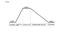
- Example 1 to 6 and Comparative Examples 1 and 2 the RTA treatment and the sacrificial oxidation treatment (thermal oxidation + thermal oxide film removal with the HF solution) were performed on the fabricated SOI wafers. Conditions are shown in Table 1. A temperature profile of thermal oxidation in the sacrificial oxidation treatment of Example 1 is shown in FIG. 2 .
- Comparative Example 3 Although the RTA treatment and the sacrificial oxidation treatment (thermal oxidation + thermal oxide film removal with the HF solution) were performed on the fabricated SOI wafers, in the first and second sacrificial oxidation treatments, post annealing (100% Ar, 1100°C, two hours)was carried out continuously after termination of thermal oxidation. A temperature profile of thermal oxidation and post annealing in the sacrificial oxidation treatment of Comparative Example 3 is shown in FIG. 3 .
- the SOI layer front surface was etched down to 30 nm with a chromium-less selective etchant and then the etch pit density was measured by an optical microscope.
- the front surface of the SOI layer after the second sacrificial oxidation treatment was measured by an AFM (measuring area: 30 ⁇ m-square).
- the present invention is not limited to the above-mentioned examples.
- the above-mentioned examples are merely illustrative and matters having configurations which are substantially identical to the technical ideas described in the scope of the patent claims of the present invention and exhibiting the same operational effects fall within the technical scope of the present invention, whatsoever they may be.
Landscapes
- Element Separation (AREA)
Applications Claiming Priority (2)
| Application Number | Priority Date | Filing Date | Title |
|---|---|---|---|
| JP2012001611A JP2013143407A (ja) | 2012-01-06 | 2012-01-06 | 貼り合わせsoiウェーハの製造方法 |
| PCT/JP2012/007690 WO2013102968A1 (fr) | 2012-01-06 | 2012-11-30 | Procédé de fabrication de tranche de silicium sur isolant (soi) fixée |
Publications (2)
| Publication Number | Publication Date |
|---|---|
| EP2802001A1 true EP2802001A1 (fr) | 2014-11-12 |
| EP2802001A4 EP2802001A4 (fr) | 2015-09-16 |
Family
ID=48745045
Family Applications (1)
| Application Number | Title | Priority Date | Filing Date |
|---|---|---|---|
| EP12864102.4A Withdrawn EP2802001A4 (fr) | 2012-01-06 | 2012-11-30 | Procédé de fabrication de tranche de silicium sur isolant (soi) fixée |
Country Status (6)
| Country | Link |
|---|---|
| US (1) | US9076840B2 (fr) |
| EP (1) | EP2802001A4 (fr) |
| JP (1) | JP2013143407A (fr) |
| KR (1) | KR20140121392A (fr) |
| CN (1) | CN104025254A (fr) |
| WO (1) | WO2013102968A1 (fr) |
Cited By (3)
| Publication number | Priority date | Publication date | Assignee | Title |
|---|---|---|---|---|
| KR20180016394A (ko) * | 2015-06-15 | 2018-02-14 | 신에쯔 한도타이 가부시키가이샤 | Soi웨이퍼의 제조방법 |
| FR3093858A1 (fr) * | 2019-03-15 | 2020-09-18 | Soitec | Procédé de transfert d’une couche utile sur un substrat support |
| FR3093860A1 (fr) * | 2019-03-15 | 2020-09-18 | Soitec | Procédé de transfert d’une couche utile sur un substrat support |
Families Citing this family (11)
| Publication number | Priority date | Publication date | Assignee | Title |
|---|---|---|---|---|
| JP6086031B2 (ja) * | 2013-05-29 | 2017-03-01 | 信越半導体株式会社 | 貼り合わせウェーハの製造方法 |
| JP6200273B2 (ja) * | 2013-10-17 | 2017-09-20 | 信越半導体株式会社 | 貼り合わせウェーハの製造方法 |
| JP6036732B2 (ja) | 2014-03-18 | 2016-11-30 | 信越半導体株式会社 | 貼り合わせウェーハの製造方法 |
| JP2016082093A (ja) * | 2014-10-17 | 2016-05-16 | 信越半導体株式会社 | 貼り合わせウェーハの製造方法 |
| JP6531743B2 (ja) * | 2016-09-27 | 2019-06-19 | 信越半導体株式会社 | 貼り合わせsoiウェーハの製造方法 |
| CN106601615B (zh) * | 2016-12-27 | 2020-05-15 | 上海新傲科技股份有限公司 | 提高键合强度的退火方法 |
| US11257902B2 (en) * | 2020-05-28 | 2022-02-22 | Taiwan Semiconductor Manufacturing Company Limited | SOI device structure for robust isolation |
| CN114664657A (zh) * | 2021-10-29 | 2022-06-24 | 中国科学院上海微系统与信息技术研究所 | 一种晶圆表面处理方法 |
| CN116053191B (zh) * | 2022-12-21 | 2024-02-09 | 中环领先半导体科技股份有限公司 | 一种绝缘体上硅衬底及其制备方法 |
| CN116387241A (zh) * | 2023-04-21 | 2023-07-04 | 中芯先锋集成电路制造(绍兴)有限公司 | 绝缘体上半导体衬底的制造方法及半导体器件的制造方法 |
| CN117096012B (zh) * | 2023-08-22 | 2024-03-26 | 中环领先半导体科技股份有限公司 | 一种氧化膜、硅片及其制备方法 |
Family Cites Families (14)
| Publication number | Priority date | Publication date | Assignee | Title |
|---|---|---|---|---|
| FR2681472B1 (fr) | 1991-09-18 | 1993-10-29 | Commissariat Energie Atomique | Procede de fabrication de films minces de materiau semiconducteur. |
| JPH11307472A (ja) | 1998-04-23 | 1999-11-05 | Shin Etsu Handotai Co Ltd | 水素イオン剥離法によってsoiウエーハを製造する方法およびこの方法で製造されたsoiウエーハ |
| JP2000124092A (ja) | 1998-10-16 | 2000-04-28 | Shin Etsu Handotai Co Ltd | 水素イオン注入剥離法によってsoiウエーハを製造する方法およびこの方法で製造されたsoiウエーハ |
| FR2797714B1 (fr) * | 1999-08-20 | 2001-10-26 | Soitec Silicon On Insulator | Procede de traitement de substrats pour la microelectronique et substrats obtenus par ce procede |
| WO2001028000A1 (fr) * | 1999-10-14 | 2001-04-19 | Shin-Etsu Handotai Co., Ltd. | Procede de fabrication d'une tranche de soi, et tranche de soi |
| CN100454552C (zh) | 2001-07-17 | 2009-01-21 | 信越半导体株式会社 | 贴合晶片的制造方法及贴合晶片、以及贴合soi晶片 |
| WO2005013318A2 (fr) | 2003-07-29 | 2005-02-10 | S.O.I.Tec Silicon On Insulator Technologies | Procede d’obtention d’une couche mince de qualite accrue par co-implantation et recuit thermique |
| EP1792338A1 (fr) | 2004-09-21 | 2007-06-06 | S.O.I.TEC. Silicon on Insulator Technologies S.A. | Procede de transfert de couche mince dans lequel une etape de co-implantation est executee selon des conditions evitant la formation de bulles et limitant la rugosite |
| EP1831922B9 (fr) | 2004-12-28 | 2010-02-24 | S.O.I.Tec Silicon on Insulator Technologies | Procede servant a obtenir une couche mince possedant une densite faible de trous |
| FR2895563B1 (fr) * | 2005-12-22 | 2008-04-04 | Soitec Silicon On Insulator | Procede de simplification d'une sequence de finition et structure obtenue par le procede |
| WO2007074550A1 (fr) * | 2005-12-27 | 2007-07-05 | Shin-Etsu Chemical Co., Ltd. | Procede de production de tranches soi et tranches soi ainsi produites |
| JP5135935B2 (ja) | 2007-07-27 | 2013-02-06 | 信越半導体株式会社 | 貼り合わせウエーハの製造方法 |
| JP5263509B2 (ja) * | 2008-09-19 | 2013-08-14 | 信越半導体株式会社 | 貼り合わせウェーハの製造方法 |
| FR2943458B1 (fr) * | 2009-03-18 | 2011-06-10 | Soitec Silicon On Insulator | Procede de finition d'un substrat de type "silicium sur isolant" soi |
-
2012
- 2012-01-06 JP JP2012001611A patent/JP2013143407A/ja active Pending
- 2012-11-30 KR KR1020147018404A patent/KR20140121392A/ko not_active Ceased
- 2012-11-30 WO PCT/JP2012/007690 patent/WO2013102968A1/fr not_active Ceased
- 2012-11-30 US US14/364,162 patent/US9076840B2/en active Active
- 2012-11-30 EP EP12864102.4A patent/EP2802001A4/fr not_active Withdrawn
- 2012-11-30 CN CN201280065462.0A patent/CN104025254A/zh active Pending
Cited By (9)
| Publication number | Priority date | Publication date | Assignee | Title |
|---|---|---|---|---|
| KR20180016394A (ko) * | 2015-06-15 | 2018-02-14 | 신에쯔 한도타이 가부시키가이샤 | Soi웨이퍼의 제조방법 |
| EP3309820A4 (fr) * | 2015-06-15 | 2019-01-23 | Shin-Etsu Handotai Co., Ltd. | Procédé de fabrication de tranche soi |
| FR3093858A1 (fr) * | 2019-03-15 | 2020-09-18 | Soitec | Procédé de transfert d’une couche utile sur un substrat support |
| FR3093860A1 (fr) * | 2019-03-15 | 2020-09-18 | Soitec | Procédé de transfert d’une couche utile sur un substrat support |
| WO2020188167A1 (fr) * | 2019-03-15 | 2020-09-24 | Soitec | Procede de transfert d'une couche utile sur un substrat support |
| WO2020188168A1 (fr) * | 2019-03-15 | 2020-09-24 | Soitec | Procede de transfert d'une couche utile sur un substrat support |
| KR20210134783A (ko) * | 2019-03-15 | 2021-11-10 | 소이텍 | 유용 층을 캐리어 기판에 전달하는 공정 |
| US11881429B2 (en) | 2019-03-15 | 2024-01-23 | Soitec | Method for transferring a useful layer onto a support substrate |
| US12142517B2 (en) | 2019-03-15 | 2024-11-12 | Soitec | Method for transferring a useful layer from a donor substrate onto a support substrate by applying a predetermined stress |
Also Published As
| Publication number | Publication date |
|---|---|
| US20140322895A1 (en) | 2014-10-30 |
| KR20140121392A (ko) | 2014-10-15 |
| CN104025254A (zh) | 2014-09-03 |
| EP2802001A4 (fr) | 2015-09-16 |
| US9076840B2 (en) | 2015-07-07 |
| WO2013102968A1 (fr) | 2013-07-11 |
| JP2013143407A (ja) | 2013-07-22 |
Similar Documents
| Publication | Publication Date | Title |
|---|---|---|
| US9076840B2 (en) | Method for manufacturing a bonded SOI wafer | |
| EP2808889B1 (fr) | Procédé de fabrication d'une plaquette de silicium sur isolant collée | |
| KR100949997B1 (ko) | 접합 웨이퍼의 제조 방법 | |
| JPWO2003009386A1 (ja) | 貼り合わせウエーハの製造方法 | |
| TWI355711B (en) | Method of producing simox wafer | |
| KR20150112968A (ko) | Soi 웨이퍼의 제조방법 및 soi 웨이퍼 | |
| US10763127B2 (en) | Heat treatment method for semiconductor wafer | |
| JP2006210899A (ja) | Soiウエーハの製造方法及びsoiウェーハ | |
| EP3007204B1 (fr) | Procédé de fabrication de tranche liée | |
| EP3016133A1 (fr) | Procédé de fabrication de plaquette liée | |
| KR20150070096A (ko) | Soi 웨이퍼의 제조방법 | |
| WO2016059748A1 (fr) | Procédé de fabrication de tranche collée | |
| JP6500845B2 (ja) | 貼り合わせウェーハの製造方法 | |
| JP2012222294A (ja) | 貼り合わせウェーハの製造方法 | |
| JP5673180B2 (ja) | 貼り合わせウェーハの製造方法 | |
| EP3043374A1 (fr) | Procédé de fabrication de plaquette liée | |
| EP1939927B1 (fr) | Procédé de production de plaquette collée | |
| JP2006013179A (ja) | Soiウェーハの製造方法 |
Legal Events
| Date | Code | Title | Description |
|---|---|---|---|
| PUAI | Public reference made under article 153(3) epc to a published international application that has entered the european phase |
Free format text: ORIGINAL CODE: 0009012 |
|
| 17P | Request for examination filed |
Effective date: 20140617 |
|
| AK | Designated contracting states |
Kind code of ref document: A1 Designated state(s): AL AT BE BG CH CY CZ DE DK EE ES FI FR GB GR HR HU IE IS IT LI LT LU LV MC MK MT NL NO PL PT RO RS SE SI SK SM TR |
|
| DAX | Request for extension of the european patent (deleted) | ||
| RA4 | Supplementary search report drawn up and despatched (corrected) |
Effective date: 20150819 |
|
| RIC1 | Information provided on ipc code assigned before grant |
Ipc: H01L 21/02 20060101AFI20150813BHEP Ipc: H01L 21/306 20060101ALI20150813BHEP Ipc: H01L 21/324 20060101ALI20150813BHEP Ipc: H01L 21/762 20060101ALI20150813BHEP Ipc: H01L 27/12 20060101ALI20150813BHEP |
|
| RAP1 | Party data changed (applicant data changed or rights of an application transferred) |
Owner name: SHIN-ETSU HANDOTAI CO., LTD. |
|
| STAA | Information on the status of an ep patent application or granted ep patent |
Free format text: STATUS: EXAMINATION IS IN PROGRESS |
|
| 17Q | First examination report despatched |
Effective date: 20170831 |
|
| STAA | Information on the status of an ep patent application or granted ep patent |
Free format text: STATUS: THE APPLICATION HAS BEEN WITHDRAWN |
|
| 18W | Application withdrawn |
Effective date: 20171127 |