EP2802017A1 - Chaîne de cellules solaires, procédé et dispositif de liaison de cellules solaires à une chaîne de cellules solaires - Google Patents
Chaîne de cellules solaires, procédé et dispositif de liaison de cellules solaires à une chaîne de cellules solaires Download PDFInfo
- Publication number
- EP2802017A1 EP2802017A1 EP13167080.4A EP13167080A EP2802017A1 EP 2802017 A1 EP2802017 A1 EP 2802017A1 EP 13167080 A EP13167080 A EP 13167080A EP 2802017 A1 EP2802017 A1 EP 2802017A1
- Authority
- EP
- European Patent Office
- Prior art keywords
- solar cell
- solar cells
- cell string
- contact element
- contact
- Prior art date
- Legal status (The legal status is an assumption and is not a legal conclusion. Google has not performed a legal analysis and makes no representation as to the accuracy of the status listed.)
- Withdrawn
Links
- 238000000034 method Methods 0.000 title claims description 15
- 239000011810 insulating material Substances 0.000 claims description 12
- 229910052751 metal Inorganic materials 0.000 claims description 12
- 239000002184 metal Substances 0.000 claims description 12
- 239000012774 insulation material Substances 0.000 claims description 11
- 238000004049 embossing Methods 0.000 claims description 10
- 238000003856 thermoforming Methods 0.000 claims description 3
- 210000004027 cell Anatomy 0.000 description 69
- 238000009413 insulation Methods 0.000 description 10
- 238000005476 soldering Methods 0.000 description 4
- RYGMFSIKBFXOCR-UHFFFAOYSA-N Copper Chemical compound [Cu] RYGMFSIKBFXOCR-UHFFFAOYSA-N 0.000 description 3
- 238000005452 bending Methods 0.000 description 3
- 229910052802 copper Inorganic materials 0.000 description 3
- 239000010949 copper Substances 0.000 description 3
- 239000000463 material Substances 0.000 description 3
- 239000002390 adhesive tape Substances 0.000 description 2
- 230000005540 biological transmission Effects 0.000 description 2
- 238000003825 pressing Methods 0.000 description 2
- 229910000679 solder Inorganic materials 0.000 description 2
- 238000003466 welding Methods 0.000 description 2
- 239000000853 adhesive Substances 0.000 description 1
- 238000004026 adhesive bonding Methods 0.000 description 1
- 230000001070 adhesive effect Effects 0.000 description 1
- 229910052782 aluminium Inorganic materials 0.000 description 1
- XAGFODPZIPBFFR-UHFFFAOYSA-N aluminium Chemical compound [Al] XAGFODPZIPBFFR-UHFFFAOYSA-N 0.000 description 1
- 238000000576 coating method Methods 0.000 description 1
- 230000000295 complement effect Effects 0.000 description 1
- 150000001875 compounds Chemical class 0.000 description 1
- 239000004020 conductor Substances 0.000 description 1
- 238000001816 cooling Methods 0.000 description 1
- 229920002457 flexible plastic Polymers 0.000 description 1
- 238000003780 insertion Methods 0.000 description 1
- 230000037431 insertion Effects 0.000 description 1
- 239000000203 mixture Substances 0.000 description 1
- 229920003023 plastic Polymers 0.000 description 1
- 238000009417 prefabrication Methods 0.000 description 1
- 238000007650 screen-printing Methods 0.000 description 1
- 238000007493 shaping process Methods 0.000 description 1
Images

Classifications
-
- H—ELECTRICITY
- H10—SEMICONDUCTOR DEVICES; ELECTRIC SOLID-STATE DEVICES NOT OTHERWISE PROVIDED FOR
- H10F—INORGANIC SEMICONDUCTOR DEVICES SENSITIVE TO INFRARED RADIATION, LIGHT, ELECTROMAGNETIC RADIATION OF SHORTER WAVELENGTH OR CORPUSCULAR RADIATION
- H10F19/00—Integrated devices, or assemblies of multiple devices, comprising at least one photovoltaic cell covered by group H10F10/00, e.g. photovoltaic modules
- H10F19/90—Structures for connecting between photovoltaic cells, e.g. interconnections or insulating spacers
- H10F19/902—Structures for connecting between photovoltaic cells, e.g. interconnections or insulating spacers for series or parallel connection of photovoltaic cells
- H10F19/904—Structures for connecting between photovoltaic cells, e.g. interconnections or insulating spacers for series or parallel connection of photovoltaic cells characterised by the shapes of the structures
-
- H—ELECTRICITY
- H10—SEMICONDUCTOR DEVICES; ELECTRIC SOLID-STATE DEVICES NOT OTHERWISE PROVIDED FOR
- H10F—INORGANIC SEMICONDUCTOR DEVICES SENSITIVE TO INFRARED RADIATION, LIGHT, ELECTROMAGNETIC RADIATION OF SHORTER WAVELENGTH OR CORPUSCULAR RADIATION
- H10F19/00—Integrated devices, or assemblies of multiple devices, comprising at least one photovoltaic cell covered by group H10F10/00, e.g. photovoltaic modules
- H10F19/90—Structures for connecting between photovoltaic cells, e.g. interconnections or insulating spacers
- H10F19/902—Structures for connecting between photovoltaic cells, e.g. interconnections or insulating spacers for series or parallel connection of photovoltaic cells
- H10F19/908—Structures for connecting between photovoltaic cells, e.g. interconnections or insulating spacers for series or parallel connection of photovoltaic cells for back-contact photovoltaic cells
-
- H—ELECTRICITY
- H10—SEMICONDUCTOR DEVICES; ELECTRIC SOLID-STATE DEVICES NOT OTHERWISE PROVIDED FOR
- H10F—INORGANIC SEMICONDUCTOR DEVICES SENSITIVE TO INFRARED RADIATION, LIGHT, ELECTROMAGNETIC RADIATION OF SHORTER WAVELENGTH OR CORPUSCULAR RADIATION
- H10F71/00—Manufacture or treatment of devices covered by this subclass
- H10F71/137—Batch treatment of the devices
- H10F71/1375—Apparatus for automatic interconnection of photovoltaic cells in a module
-
- Y—GENERAL TAGGING OF NEW TECHNOLOGICAL DEVELOPMENTS; GENERAL TAGGING OF CROSS-SECTIONAL TECHNOLOGIES SPANNING OVER SEVERAL SECTIONS OF THE IPC; TECHNICAL SUBJECTS COVERED BY FORMER USPC CROSS-REFERENCE ART COLLECTIONS [XRACs] AND DIGESTS
- Y02—TECHNOLOGIES OR APPLICATIONS FOR MITIGATION OR ADAPTATION AGAINST CLIMATE CHANGE
- Y02E—REDUCTION OF GREENHOUSE GAS [GHG] EMISSIONS, RELATED TO ENERGY GENERATION, TRANSMISSION OR DISTRIBUTION
- Y02E10/00—Energy generation through renewable energy sources
- Y02E10/50—Photovoltaic [PV] energy
-
- Y—GENERAL TAGGING OF NEW TECHNOLOGICAL DEVELOPMENTS; GENERAL TAGGING OF CROSS-SECTIONAL TECHNOLOGIES SPANNING OVER SEVERAL SECTIONS OF THE IPC; TECHNICAL SUBJECTS COVERED BY FORMER USPC CROSS-REFERENCE ART COLLECTIONS [XRACs] AND DIGESTS
- Y10—TECHNICAL SUBJECTS COVERED BY FORMER USPC
- Y10T—TECHNICAL SUBJECTS COVERED BY FORMER US CLASSIFICATION
- Y10T29/00—Metal working
- Y10T29/53—Means to assemble or disassemble
- Y10T29/5313—Means to assemble electrical device
- Y10T29/532—Conductor
- Y10T29/53209—Terminal or connector
Definitions
- the invention relates to a solar cell string, a method and an apparatus for connecting solar cells to a solar cell string.
- the invention is particularly suitable for connecting so-called rear-side solar cells, which are characterized in that the contact zones, i. the p-doped and n-doped regions are located on the same side of the solar cell.
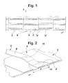
- FIG. 1 shows a generic comparable comparable solar cell string according to the prior art. Details on the structure and design of the connection arrangement of the known solar cell string are made FIG. 2 removable, which relates to a string of backside solar cells. For electrically connecting the solar cells, a copper band created by bending forming is used. On the back side of the solar cell, an insulating strip 4 extending in the x-direction is arranged, which has openings 5, wherein the openings release n-doped contact zones 10. The zone 10 is familiar to the person skilled in the art under the English term "n-pad”.
- the contact element 3 is designed as a bent part and has bending edges, which are indicated by the transverse to the x-direction parallel lines 11.
- the known contact elements are comparatively narrow; the maximum width of the contact element 3 is limited by the opening diameter d. Such narrow contact elements lead to an undesirable loss of power because of the relatively high ohmic resistance.
- the compounds of the solar cells should be characterized by low ohmic losses.
- the efficiency of a constructed from one or more such solar cell strings solar module should be optimized.
- a solar cell string having the features of claim 1.
- Several solar cells strung together along a longitudinal direction are preferably electrically connected to contact elements formed in each case from a metal strip (eg of copper).
- a contact element connects respectively two adjacent solar cells with each other.
- the solar cells are provided with an insulating material, which in each case has at least one opening, via which the contact element contacts the solar cells.
- the insulating material may be a longitudinally extending band.
- a preferably one-sided adhesive insulating tape can be used for the insulation, which consists for example of an electrically non-conductive or only slightly conductive plastic material.
- Such an adhesive tape can be easily fixed by pressing on the solar cell surface to the solar cell.
- insulation bands to the solar cells would be conceivable.
- the solar cell could therefore be provided with approximately equal-sized strips of solder mask. Insulation material could also be applied to the solar cells in a different coating process or in another way. If the solar cells have a plurality of rows of n-poles, then the solar cells may preferably be provided with a corresponding number of insulating tapes applied thereto.
- the contact has a recess accommodated in the at least one opening for creating the contact between the contact element and the solar cell, there are several advantages. Thanks to the recessed contact elements wider contact elements can be used, whereby the transmission power can be increased considerably as a result of reduced ohmic loss. Thus, the efficiency of a solar module constructed from such solar cell strings can be improved. Depending on the configuration of the depression, it is finally possible to achieve improved contact between the contact element and the solar cell.
- the depression is a cup-shaped depression, which is preferably created by a deep-drawing or embossing process in the metal strip. Such cup-like depressions can be easily produced.
- the depression may have a flat cup bottom.
- the opening and / or the recess associated with the opening may be circular in relation to a plan view.
- an opening of a circular hole is particularly preferably associated with an approximately complementary, circular recess.
- the opening could, for example, be oval.
- polygonal opening forms and deepening forms are particularly advantageously, the opening and recess are similarly shaped, with the recess should be smaller than the opening in the rule. As long as the recess fits into the opening, even different shapes would be conceivable.
- the contact element overlaps the at least one opening on all sides, with respect to the plan view, in each case. If the respective contact element in a plan view is wider than the opening, an energetically particularly efficient solar cell string results.
- the arrangement can be further optimized if the contact element is in each case at least 25%, preferably at least 50%, and particularly preferably approximately 100% wider, relative to the diameter of the at least one opening.
- the solar cells of the solar cell string could even be equipped with even wider contact elements.
- the respective contact element can each have, in the region of a recess, at least one surface section which lies on the insulation material.
- the recess is raised relative to the mentioned surface portion.
- the depth of the recess would thus correspond to the thickness of the insulating material.
- depth of the depression is greater than the thickness of the insulation material, which results in a distance or air gap between the solar cell surface and the surface portion of the insulation material.
- the respective contact element may have at least two surface sections, which are connected via an exposed, spaced from the solar cell bridge portion.
- the contact element has correspondingly preferably two recesses raised relative to the surface sections.
- Another aspect of the invention relates to a method for connecting solar cells and in particular for connecting rear-side solar cells to a solar cell string, in particular the previously described solar cell string.
- the method comprises the following steps: At least in regions, apertured, prefabricated insulation material in the form of an insulating tape is applied to the solar cells. For example, provided with openings provided insulation bands. These insulation bands are each placed on the solar cells in such a way that the openings release the n-contact zones.
- the contact elements are produced by recesses are introduced in metal strips by a deep-drawing or embossing process. Thereafter, the solar cells can be equipped with the contact elements produced in this way, wherein the recesses are inserted into the respective openings during the assembly process.
- a further aspect of the invention finally relates to a device for electrically connecting solar cells by means of contact elements, preferably for carrying out the previously described method.
- the apparatus comprises an applicator unit for applying apertured insulation material to the solar cells and an embossing or deep drawing unit having at least one stamper for creating openings adapted to the opening in contact elements formed of metal bands.
- a respective contact element may have a plurality of recesses. So that the recesses can be created in one operation, it may be advantageous if the embossing or thermoforming unit has a plurality of dies. Of course, it would also be conceivable to apply the depressions with a single stamping die per contact element.
- the one or more dies may be formed as a knob-like elevations, which can be particularly easily cup-like depressions introduced into a metal strip.
- FIG. 3 shows a contact between solar cell 2 and contact element 3 of a solar cell string according to the invention. Except for the contact elements described in detail below, the solar cell string is approximately the same as the one out of FIG. 1 built up. By means of such contact elements 3 backside solar cells 2 are electrically connected.
- FIG. 3 shows, on the solar cell 2 in the region of the n-pole, the known per se, in the longitudinal direction x extending insulating tape 4 is arranged (see. FIG. 2 ).
- the insulating strip consists essentially of an electrically non or only slightly conductive material, for example of a flexible plastic material.
- the insulating material can be designed as an adhesive tape, so that it can be applied to the solar cells in a particularly simple manner and in a single working step (by pressing). Such insulation bands are cheap and available in different widths, thicknesses and compositions and optimally adapted to the particular application.
- the insulating tape 4 has at least one opening 5, via which the contact element 3 contacts the solar cell 2 in the n-doped contact zone.
- the opening 5 makes it possible to expose the contact zone designated by 10 ("n-pad"), whereby a contacting of the solar cell 2 by the contact element 3 is made possible.
- the contact element 3 has a cup-shaped depression 6 which can be created in a simple manner by a deep-drawing or embossing process, for example using a stamping die.
- the contact element 3 is made of a metal strip with a width B, the cut and by Abkantvone or another forming process is preformed.
- This shaping strain relief structures are created. These strain relief structures can prevent or at least reduce undesired, thermally influenced expansion or bending of the solar cells occurring when the contact is completed by, for example, soldering or welding.
- copper tapes can be used, which are tinned (coated with solder) or silvered.
- each insulation band assigned to each solar cell has a plurality of openings, each opening being assigned an n-doped contact zone. Accordingly, the associated contact element, however, also has a plurality of recesses 6 corresponding to the number of openings.
- the solar cell string per solar cell have a plurality of mutually parallel contact elements.
- the solar cell string can have three contact rows extending in the longitudinal direction with contact elements arranged in pairs. Each of the three contact element pairs comprises two contact elements which are oriented in the opposite direction in accordance with the alternating attachment of the insulation material (cf. Fig. 1 ).
- the recess 6 has to create an electrically advantageous contact surface on a flat cup bottom 7. Both the opening 5 and the recess 6 associated with the opening are circular in relation to the top view.
- the cup diameter D is slightly smaller than the opening diameter d, so that on the one hand a simple insertion of the recess in the opening and a secure electrical connection (eg by means of soldering, gluing, and / or welding) is ensured.
- the contact element 3 shown here is wider than the opening 5 in the insulating material 4, whereby the transmission power of the solar cell connections can be significantly improved. In other words, the contact element 3 overlaps the opening 5.
- the diameter of the opening 5 is designated by d.
- the width of the contact element can thus be decoupled from the width of the n-pad, which widens the design options and freedoms for designing and dimensioning the contact elements.
- the contact elements 3 are about twice as wide as the diameter d of the openings 5. Very good results can be but already achieve when the contact elements with respect to the diameter of the openings 5 are at least 25% wider. This makes it possible, for example, to contact a 2 mm wide n-pad 10 with a 4 or 5 mm wide contact element 4, which results in high module efficiency, which results in high cell efficiency. Consequently, both cell efficiency and module efficiency can be maximized.
- the contact element 3 has in the region of each recess 6 each have a surface portion 9 which lies on the insulating material 4.
- the depth of the recess thus corresponds to the thickness of the band-shaped insulating material 4.
- the surface portions 9 are connected via exposed, spaced from the solar cell bridge sections 8.
- the invention is characterized in that it comprises a stamping or deep drawing unit (not shown), with which depressions can be introduced into contact elements consisting of metal strips.
- the device may further comprise an applicator unit for applying insulation material preferably present as an insulation tape to the solar cells.
- the insulation tape can already be provided with openings that are created in a prefabrication process.
- the aforementioned device comprises means for creating openings (for example a perforation station) in the insulation band.
- the solar cells equipped with contact elements can pass a soldering station (not shown) with a preheating zone, in which the contacts are completed.
- the soldering station may be downstream of a cooling area.
Landscapes
- Photovoltaic Devices (AREA)
- Engineering & Computer Science (AREA)
- Manufacturing & Machinery (AREA)
Priority Applications (3)
| Application Number | Priority Date | Filing Date | Title |
|---|---|---|---|
| EP13167080.4A EP2802017A1 (fr) | 2013-05-08 | 2013-05-08 | Chaîne de cellules solaires, procédé et dispositif de liaison de cellules solaires à une chaîne de cellules solaires |
| US14/258,090 US20140332050A1 (en) | 2013-05-08 | 2014-04-22 | Solar cell string, method and device for connecting solar cells to a solar cell string |
| CN201410190670.4A CN104143577A (zh) | 2013-05-08 | 2014-05-07 | 太阳能电池串、用于将太阳能电池连接成太阳能电池串的方法和装置 |
Applications Claiming Priority (1)
| Application Number | Priority Date | Filing Date | Title |
|---|---|---|---|
| EP13167080.4A EP2802017A1 (fr) | 2013-05-08 | 2013-05-08 | Chaîne de cellules solaires, procédé et dispositif de liaison de cellules solaires à une chaîne de cellules solaires |
Publications (1)
| Publication Number | Publication Date |
|---|---|
| EP2802017A1 true EP2802017A1 (fr) | 2014-11-12 |
Family
ID=48288935
Family Applications (1)
| Application Number | Title | Priority Date | Filing Date |
|---|---|---|---|
| EP13167080.4A Withdrawn EP2802017A1 (fr) | 2013-05-08 | 2013-05-08 | Chaîne de cellules solaires, procédé et dispositif de liaison de cellules solaires à une chaîne de cellules solaires |
Country Status (3)
| Country | Link |
|---|---|
| US (1) | US20140332050A1 (fr) |
| EP (1) | EP2802017A1 (fr) |
| CN (1) | CN104143577A (fr) |
Families Citing this family (1)
| Publication number | Priority date | Publication date | Assignee | Title |
|---|---|---|---|---|
| CN109560155B (zh) * | 2018-12-29 | 2023-09-22 | 苏州阿特斯阳光电力科技有限公司 | 太阳能电池组件及其制造方法 |
Citations (4)
| Publication number | Priority date | Publication date | Assignee | Title |
|---|---|---|---|---|
| EP0095843A2 (fr) * | 1982-05-28 | 1983-12-07 | AMP INCORPORATED (a New Jersey corporation) | Système d'interconnexion pour cellules photovoltaiques |
| US20030127124A1 (en) * | 2002-01-04 | 2003-07-10 | Jones Bernard D. | Solar cell stringing machine |
| WO2009097161A1 (fr) * | 2008-01-31 | 2009-08-06 | Global Solar Energy, Inc. | Chaîne de cellules solaires à couches minces |
| WO2013001822A1 (fr) * | 2011-06-28 | 2013-01-03 | パナソニック株式会社 | Module de cellules solaires |
-
2013
- 2013-05-08 EP EP13167080.4A patent/EP2802017A1/fr not_active Withdrawn
-
2014
- 2014-04-22 US US14/258,090 patent/US20140332050A1/en not_active Abandoned
- 2014-05-07 CN CN201410190670.4A patent/CN104143577A/zh active Pending
Patent Citations (4)
| Publication number | Priority date | Publication date | Assignee | Title |
|---|---|---|---|---|
| EP0095843A2 (fr) * | 1982-05-28 | 1983-12-07 | AMP INCORPORATED (a New Jersey corporation) | Système d'interconnexion pour cellules photovoltaiques |
| US20030127124A1 (en) * | 2002-01-04 | 2003-07-10 | Jones Bernard D. | Solar cell stringing machine |
| WO2009097161A1 (fr) * | 2008-01-31 | 2009-08-06 | Global Solar Energy, Inc. | Chaîne de cellules solaires à couches minces |
| WO2013001822A1 (fr) * | 2011-06-28 | 2013-01-03 | パナソニック株式会社 | Module de cellules solaires |
Also Published As
| Publication number | Publication date |
|---|---|
| CN104143577A (zh) | 2014-11-12 |
| US20140332050A1 (en) | 2014-11-13 |
Similar Documents
| Publication | Publication Date | Title |
|---|---|---|
| DE2502214C2 (de) | Verfahren zur Herstellung von laminierten Sammelschienen | |
| DE3149641A1 (de) | "eleketrische schaltungsplatte und verfahren zu ihrer herstellung" | |
| DE102009044060B4 (de) | Solarzellenkontaktierungsverfahren, Solarzellenanordnung, Solarzellenstring und Solarzellenmodul | |
| DE10046489C1 (de) | Lötbares elektrisches Anschlußelement mit Lotdepot und dessen Verwendung | |
| DE102010002521A1 (de) | Solarzelle mit spezieller Busbarform, diese Solarzelle enthaltende Solarzellenanordnung sowie Verfahren zur Herstellung der Solarzelle | |
| DE2855838C2 (de) | Bauteilanordnung | |
| DE10221085B4 (de) | Baugruppe mit einer Verbindungseinrichtung zum Kontaktieren eines Halbleiter-Bauelements und Herstellungsverfahren | |
| DE102012222364A1 (de) | Steckverbinder und Vorrichtung mit einem solchen Steckverbinder | |
| EP2802017A1 (fr) | Chaîne de cellules solaires, procédé et dispositif de liaison de cellules solaires à une chaîne de cellules solaires | |
| DE102013202551A1 (de) | Verfahren zur Herstellung eines Substrats mit einer Kavität | |
| DE1909480A1 (de) | Halbleiterbauelement und Verfahren zu seiner Herstellung | |
| WO2017144691A1 (fr) | Élément optoélectronique pourvu d'une section grille de connexion | |
| DE102011051511A1 (de) | Rückkontaktsolarzelle und Verfahren zum Herstellen einer solchen | |
| JP2021057139A (ja) | バスバーアッセンブリ及びその製造方法 | |
| DE202008011461U1 (de) | Elektrische Solarzellenverbindungen sowie photovoltaische Solarmodule | |
| DE102015204915B4 (de) | Wärmeleitkörper mit einer Koppeloberfläche mit Vertiefung und Wärmetransfervorrichtung | |
| WO2013026527A1 (fr) | Substrat de montage d'éléments électroniques | |
| EP2820673B1 (fr) | Substrat comportant un ilot pour puces agrandi | |
| EP2529398B1 (fr) | Amélioration de la planéité par des découpes non guidées sur les estampages | |
| DE1614567C3 (de) | Halbleiterbauelement und Verfahren zu seiner Herstellung | |
| EP2492957B1 (fr) | Agencement de circuit | |
| DE102015119082B4 (de) | Solarzellenkontakt-Herstellungsverfahren, Solarzellen-Herstellungsverfahren und Solarzelle | |
| DE102010039563A1 (de) | Solarzellenverbund mit mehreren Solarzellen | |
| DE112019002169B4 (de) | Verfahren zur Herstellung einer elektronischen Chipkarte und eine mit diesem Verfahren hergestellte Chipkarte | |
| EP4320678A1 (fr) | Accumulateur d'énergie électrique doté d'un système de contact à cellules latérales et véhicule à moteur |
Legal Events
| Date | Code | Title | Description |
|---|---|---|---|
| PUAI | Public reference made under article 153(3) epc to a published international application that has entered the european phase |
Free format text: ORIGINAL CODE: 0009012 |
|
| 17P | Request for examination filed |
Effective date: 20130508 |
|
| AK | Designated contracting states |
Kind code of ref document: A1 Designated state(s): AL AT BE BG CH CY CZ DE DK EE ES FI FR GB GR HR HU IE IS IT LI LT LU LV MC MK MT NL NO PL PT RO RS SE SI SK SM TR |
|
| AX | Request for extension of the european patent |
Extension state: BA ME |
|
| STAA | Information on the status of an ep patent application or granted ep patent |
Free format text: STATUS: THE APPLICATION IS DEEMED TO BE WITHDRAWN |
|
| 18D | Application deemed to be withdrawn |
Effective date: 20150513 |