EP2802081A1 - Procédé et dispositif d'annulation de brouillage et dispositif de filtrage - Google Patents
Procédé et dispositif d'annulation de brouillage et dispositif de filtrage Download PDFInfo
- Publication number
- EP2802081A1 EP2802081A1 EP12865951.3A EP12865951A EP2802081A1 EP 2802081 A1 EP2802081 A1 EP 2802081A1 EP 12865951 A EP12865951 A EP 12865951A EP 2802081 A1 EP2802081 A1 EP 2802081A1
- Authority
- EP
- European Patent Office
- Prior art keywords
- filter
- integrated
- signal
- transmitted signal
- receiving
- Prior art date
- Legal status (The legal status is an assumption and is not a legal conclusion. Google has not performed a legal analysis and makes no representation as to the accuracy of the status listed.)
- Granted
Links
Images





Classifications
-
- H—ELECTRICITY
- H04—ELECTRIC COMMUNICATION TECHNIQUE
- H04B—TRANSMISSION
- H04B1/00—Details of transmission systems, not covered by a single one of groups H04B3/00 - H04B13/00; Details of transmission systems not characterised by the medium used for transmission
- H04B1/06—Receivers
- H04B1/10—Means associated with receiver for limiting or suppressing noise or interference
-
- H—ELECTRICITY
- H04—ELECTRIC COMMUNICATION TECHNIQUE
- H04L—TRANSMISSION OF DIGITAL INFORMATION, e.g. TELEGRAPHIC COMMUNICATION
- H04L5/00—Arrangements affording multiple use of the transmission path
- H04L5/14—Two-way operation using the same type of signal, i.e. duplex
- H04L5/1461—Suppression of signals in the return path, i.e. bidirectional control circuits
-
- H—ELECTRICITY
- H04—ELECTRIC COMMUNICATION TECHNIQUE
- H04B—TRANSMISSION
- H04B1/00—Details of transmission systems, not covered by a single one of groups H04B3/00 - H04B13/00; Details of transmission systems not characterised by the medium used for transmission
- H04B1/38—Transceivers, i.e. devices in which transmitter and receiver form a structural unit and in which at least one part is used for functions of transmitting and receiving
- H04B1/40—Circuits
- H04B1/44—Transmit/receive switching
-
- H—ELECTRICITY
- H04—ELECTRIC COMMUNICATION TECHNIQUE
- H04B—TRANSMISSION
- H04B1/00—Details of transmission systems, not covered by a single one of groups H04B3/00 - H04B13/00; Details of transmission systems not characterised by the medium used for transmission
- H04B1/38—Transceivers, i.e. devices in which transmitter and receiver form a structural unit and in which at least one part is used for functions of transmitting and receiving
- H04B1/40—Circuits
- H04B1/50—Circuits using different frequencies for the two directions of communication
- H04B1/52—Hybrid arrangements, i.e. arrangements for transition from single-path two-direction transmission to single-direction transmission on each of two paths or vice versa
- H04B1/525—Hybrid arrangements, i.e. arrangements for transition from single-path two-direction transmission to single-direction transmission on each of two paths or vice versa with means for reducing leakage of transmitter signal into the receiver
-
- H—ELECTRICITY
- H04—ELECTRIC COMMUNICATION TECHNIQUE
- H04W—WIRELESS COMMUNICATION NETWORKS
- H04W28/00—Network traffic management; Network resource management
- H04W28/02—Traffic management, e.g. flow control or congestion control
- H04W28/04—Error control
Definitions
- the present invention relates to the field of radio communication and, in particular, to an interference cancellation method and apparatus, and a filter device.
- duplexer In duplex radio communication, to make a transmitter and a receiver in a frequency division multiplexing (Frequency Division Multiplexing, FDM) system share an antenna, a duplexer needs to distinguish a transmitted signal from a received signal.
- the duplexer is composed of a transmitter filter, a receiver filter, a combinational circuit, and so on.
- the combinational circuit includes reactive components such as transmission line, resistor, and capacitor.
- the combinational circuit is essentially a phasing circuit that can reduce mutual impact between the transmitter filter and the receiver filter.
- duplexers include cavity duplexer, dielectric duplexer, surface acoustic wave (Surface Acoustic Wave, SAW) filter, bulk acoustic resonator (Bulk Acoustic Resonator, BAR), and film bulk acoustic resonator (Film Bulk Acoustic Resonator, FBAR).
- SAW Surface Acoustic Wave
- BAR Bulk Acoustic Resonator
- FBAR Film Bulk Acoustic Resonator
- the FBAR is a duplexer based on a bulk acoustic resonance technology, and converts the electric energy into acoustic waves to generate resonance through a converse piezoelectric effect of a piezoelectric film.
- the wave velocity of the acoustic wave is less than the wave velocity of the electromagnetic wave by about 5 orders of magnitude.
- the size of the FBAR may be far less than the size of the electromagnetic-based dielectric porcelain device. Meanwhile, because the bulk acoustic wave has a greater power bearing capability than the surface acoustic wave, the FBAR has a better power capacity feature than the surface acoustic filter.
- LNA Low Noise Amplifier
- variable gain amplifier variable gain amplifier
- intermediate frequency filter intermediate frequency filter
- a solution to reducing the suppression requirement imposed by the transmitter onto the receiver in the prior art is to simulate interference cancellation.
- an amplitude phase regulator adjusts the phase of the transmitted signal that is coupled from the transmitting channel in a interference cancellation channel, and outputs the signal; on the receiver side, the transmitted signal whose phase is adjusted by the amplitude phase regulator is overlaid with the transmitted signal leaked from the transmitting filter on the transmitting channel, thereby cancelling the interference caused by the transmitted signal onto the received signal.
- the inventors of the present invention through their research find that in the prior art, due to the outband (band outside the transmitting band) filter feature of the transmitting filter on the transmitting channel, the outband amplitude and phase response fluctuates sharply, the delay changes sharply, but the receiving band of the receiving filter in the interference cancellation channel is a passband (a passband is a band outside the transmitting band of the transmitting filter), and the amplitude and phase response of the receiving filter is relatively constant compared with the outband amplitude and phase response of the transmitting filter on the transmitting channel.
- the amplitude phase regulator can adjust the phase of the transmitted signal output by the transmitting filter on the interference cancellation channel, the phase of the transmitted signal is not necessarily opposite to the phase of the transmitted signal output by the transmitting filter on the transmitting channel after the phase is adjusted. Consequently, the interference caused by the transmitted signal onto the received signal is not cancelled, and even may be exacerbated.
- the phase of the transmitted signal coupled from the transmitting channel is just the same as the phase of the transmitted signal output by the transmitting filter on the transmitting channel. In this case, the interference caused by the transmitted signal onto the received signal is not cancelled, and even increased drastically.
- An interference cancellation method and apparatus and also a filter device are provided in embodiments of the present invention to cancel the interfering signals leaked to the receiving channel, and enable the receiving channel to suppress the transmitted signal.
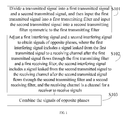
- An interference cancellation method provided in an embodiment of the present invention includes: dividing a transmitted signal into a first transmitted signal and a second transmitted signal, and then inputting the first transmitted signal into a first transmitting filter and inputting the second transmitted signal into a second transmitting filter symmetric to the first transmitting filter;
- the first interfering signal includes a signal leaked from the first transmitted signal to a receiving channel after the first transmitted signal flows through the first transmitting filter and a first receiving filter
- the second interfering signal includes a signal leaked from the second transmitted signal to the receiving channel after the second transmitted signal flows through the second transmitting filter and a second receiving filter
- the receiving channel is a channel for a receiver to receive signals
- an interference cancellation apparatus provided in an embodiment of the present invention includes:
- a signal dividing module configured to divide a transmitted signal into a first transmitted signal and a second transmitted signal, and then input the first transmitted signal into a first transmitting filter and input the second transmitted signal into a second transmitting filter symmetric to the first transmitting filter;
- a phasing module configured to adjust a first interfering signal and a second interfering signal to obtain signals of opposite phases, where the first interfering signal includes a signal leaked from the first transmitted signal to a receiving channel after the first transmitted signal flows through the first transmitting filter and a first receiving filter, the second interfering signal includes a signal leaked from the second transmitted signal to the receiving channel after the second transmitted signal flows through the second transmitting filter and a second receiving filter, and the receiving channel is a channel for a receiver to receive signals; and
- a combining module configured to combine the signals of opposite phases.
- a filter device provided in an embodiment of the present invention includes a first duplexer and a second duplexer.
- the first duplexer includes a first receiving filter and a first transmitting filter
- the second duplexer includes a second receiving filter and a second transmitting filter.
- the first transmitting filter is symmetric to the second transmitting filter; or, the first receiving filter is symmetric to the second receiving filter and the first transmitting filter is symmetric to the second transmitting filter.
- a filter device provided in an embodiment of the present invention includes a first receiving filter, a first transmitting filter, and a duplexer.
- the duplexer includes a second receiving filter and a second transmitting filter, where the first transmitting filter is symmetric to the second transmitting filter; or, the first receiving filter is symmetric to the second receiving filter and the first transmitting filter is symmetric to the second transmitting filter.
- a filter device provided in an embodiment of the present invention includes a first transmitting filter and a second transmitting filter.
- the first transmitting filter and the second transmitting filter are integrated on the same chip, or integrated on the same substrate, or integrated in the same package, or integrated in the same module.
- a filter device provided in an embodiment of the present invention includes a first receiving filter and a second receiving filter.
- the first receiving filter and the second receiving filter are integrated on the same chip, or integrated on the same substrate, or integrated in the same package, or integrated in the same module.
- a filter device provided in an embodiment of the present invention includes a first duplexer and a second duplexer.
- the first duplexer and the second duplexer are integrated on the same chip, or integrated on the same substrate, or integrated in the same package, or integrated in the same module.
- a filter device provided in an embodiment of the present invention includes a first receiving filter, a first transmitting filter, and a duplexer.
- the duplexer, the first receiving filter, and the first transmitting filter are integrated on the same chip, or integrated on the same substrate, or integrated in the same package, or integrated in the same module.
- a base station provided in an embodiment of the present invention includes the interference cancellation apparatus provided above.
- a communication system provided in an embodiment of the present invention includes the base station provided above.
- the first transmitted signal is input into the first transmitting filter
- the second transmitted signal is input into the second transmitting filter
- the first transmitting filter is symmetric to the second transmitting filter
- the interfering signals output from the first transmitting filter and the second transmitting filter are finally adjusted to become signals of opposite phases, and are combined. Therefore, the method and the apparatus provided herein can cancel the interfering signals leaked to the receiving channel, the receiving channel suppresses the transmitted signal effectively, and the interference caused by the transmitted signal onto the received signal is cancelled.
- a and/or B refers to A, or B, or both A and B;
- A/B generally refers to "A or B", where A and B represent the objects before and after “and/or” and "/”.
- FIG. 1 is a schematic flowchart of an interference cancellation method according to an embodiment of the present invention.
- the method shown in FIG. 1 is applicable to a transceiver in an FDM system, and includes the following steps:
- a transmitted signal refers to a signal output from a digital processing unit of a transceiver, processed by the modules such as digital-to-analog converter, frequency mixer, filter, and amplifier on the transmitting channel, and to be transmitted from antenna port; and a received signal refers to a signal received from the antenna port, to be processed by the modules such as amplifier, filter, frequency mixer, and analog-to-digital converter on the receiving channel, and to be input into the digital processing unit of the transceiver.
- the transceiver is applied to a frequency division duplexing (Frequency Division Duplexing, FDD) band, and the transmitted signal and the received signal share an antenna.
- FDD Frequency Division Duplexing
- the band occupied by the transmitted signal (namely, transmitting band) alternates with the band occupied by the received signal (namely, receiving band), or, the passband of the transmitter is the stopband of the receiver, or, the stopband of the transmitter is the passband of the receiver.
- the transmitting channel refers to a channel for the transmitter to transmit signals
- the receiving channel refers to a channel for the receiver to receive signals. It should be noted that because the receiving band is a main band occupied by the received signals, the receiving band is generally used to represent the receiving channel, or the receiving channel represents the receiving band; it is the same with the relationship between the transmitting band and the transmitting channel.
- part of the transmitted signals and/or intermodulation signals derived from the transmitted signals may be leaked to the receiving channel, and cause interference onto the received signals. Suppression of the interference is also known as suppression performed by the receiving channel for the transmitted signals.
- the first transmitting filter and the second transmitting filter may be, but are not limited to, the FBAR or SAW.
- Other filters of a small size, such as BAW, may be used as the first transmitting filter and the second transmitting filter instead.
- FBAR, SAW and BAW employ a wafer cutting process. In the cutting process, two adjacent filters or duplexers on the wafer may be set onto the same chip (die or chip) through cutting. In this way, it is easy to ensure consistent electric performance between two filters or duplexers located on the same chip.
- the first transmitting filter and the second transmitting filter may be located on the same chip, and the first transmitting filter is symmetric to the second transmitting filter.
- the first transmitting filter is symmetric to the second transmitting filter. That is, the first transmitting filter and the second transmitting filter have symmetrically the same structure and features.
- the features such as transmission response delay, phase and amplitude of the first transmitting filter are the same as those of the second transmitting filter.
- the symmetry between the first transmitting filter and the second transmitting filter is not limited to the phenomenon that the first transmitting filter and the second transmitting filter have the same structure and features.
- Consistent electric performance means that: The electric performance is completely the same, or, the impact caused by the electric performance difference onto the interference cancellation result is in an acceptable range, and a certain deviation is allowed. Understandably, in “the same structure and features", the meanings of word “same” also cover the scenario that the impact caused by the difference of the structure or features onto the interference cancellation result is in an acceptable range. With the same structure and features, consistent electric performance is ensured.
- the definition of "symmetric” is also applicable to other embodiments of the present invention.
- the electric performance may include transmission response delay, phase, amplitude, and so on.
- the first transmitting filter and the second transmitting filter may be integrated on the same chip (die or chip), or integrated on the same substrate (substrate), or integrated in the same package (package), or integrated in the same module (module). In all embodiments of the present invention, it is assumed that the first transmitting filter and the second transmitting filter are integrated on the same substrate.
- a divider may be applied.
- a 90° divider or a 3dB electric bridge divides the transmitted signal into a first transmitting signal and a second transmitted signal between which the phase difference is 90°; and then the first transmitting signal and the second transmitted signal, between which the phase difference is 90°, are input into the first duplexer and the second duplexer respectively, and then output by the first duplexer and the second duplexer.
- power of the signals input into the first duplexer and the second duplexer is lower than power of the undivided signal (theoretically, regardless of loss, the power of the signals input into the first duplexer and the second duplexer respectively is half of the power of the undivided signal). In this way, the power capacity requirement on the transmitting filter in the first duplexer or the second duplexer is lowered.
- the first duplexer and the second duplexer may be integrated on the same substrate such as a silicon wafer semiconductor substrate; the first duplexer and the second duplexer that are integrated on the same substrate may be an FBAR or SAW, or may be a BAW; the first duplexer includes a first transmitting filter and a first receiving filter, and the second duplexer includes a second transmitting filter and a second receiving filter; and the symmetry between the first duplexer and the second duplexer includes symmetry between the first transmitting filter and the second transmitting filter, or includes symmetry between the first transmitting filter and the second transmitting filter, and symmetry between the first receiving filter and the second receiving filter.
- symmetry between the first transmitting filter and the second transmitting filter refers to consistent electric performance between the first transmitting filter and the second transmitting filter
- symmetry between the first receiving filter and the second receiving filter refers to consistent electric performance between the first receiving filter and the second receiving filter.
- consistent electric performance include: The electric performance is completely the same, or, the impact caused by the difference of the electric performance onto the interference cancellation result is in an acceptable range.
- the electric performance may include transmission response delay, phase, amplitude, and so on.
- the structure and features being the same is one of the scenarios of consistent electric performance. That is, symmetry scenarios include the scenario of the structure and features being the same.
- the first transmitted signal input into the first duplexer is output from the first transmitting filter of the first duplexer
- the second transmitted signal input into the second duplexer is output from the second transmitting filter of the second duplexer.
- the two transmitted signals may be input into a 90° combiner-divider connected with the first duplexer and the second duplexer.
- the signals are combined in the combiner-divider, and the combined transmitted signal is output from the antenna port.
- the signal received from the antenna port is divided through the 90° combiner-divider.
- the divided signals are input into the first duplexer and the second duplexer for filtering, and then the signals pass through another 90° combiner-divider and are input into other devices on the receiving channel.
- a coupler may couple part of the transmitted signal as the first transmitted signal, and input the first transmitted signal into the first receiving filter; the first receiving filter filters the first transmitted signal, and inputs it into the first transmitting filter, and then the first transmitting filter inputs the signal into the receiving channel.
- the first receiving filter, the first transmitting filter, and the duplexer inclusive of the second receiving filter and the second transmitting filter may be integrated on the same substrate such as a silicon wafer semiconductor substrate; the first receiving filter, the first transmitting filter, and the duplexer that are integrated on the same substrate may be an FBAR or SAW, or may be a BAW.
- the first transmitting filter is symmetric to the second transmitting filter of the duplexer; or, the first transmitting filter is symmetric to the second transmitting filter of the duplexer, and the first receiving filter is symmetric to the second receiving filter of the duplexer.
- symmetry or “symmetric”, see the definition above. That is, symmetry between the first transmitting filter and the second transmitting filter of the duplexer refers to consistent electric performance between the first transmitting filter and the second transmitting filter of the duplexer, and symmetry between the first receiving filter and the second receiving filter of the duplexer refers to consistent electric performance between the first receiving filter and the second receiving filter of the duplexer.
- the meanings of "consistent electric performance” include: The electric performance is completely the same, or, the impact caused by the difference of the electric performance onto the interference cancellation result is in an acceptable range.
- the electric performance may include transmission response delay, phase, amplitude, and so on.
- the structure and features being the same is one of the scenarios of consistent electric performance. That is, symmetry scenarios include the scenario of the structure and features being the same.
- the first receiving filter, the first transmitting filter, and the duplexer inclusive of the second receiving filter and the second transmitting filter may also be integrated on the same chip (die or chip), or integrated in the same package (package), or integrated in the same module (module) so as to accomplish consistent electric performance between the first transmitting filter and the second transmitting filter in the duplexer, or, further, accomplish consistent electric performance between the first receiving filter and the second receiving filter in the duplexer.
- the first receiving filter, the first transmitting filter and the duplexer inclusive of the second receiving filter and the second transmitting filter are integrated on the same substrate.
- the signal not coupled by the coupler in the transmitted signal may be input as a second transmitted signal into the duplexer which is integrated with the first transmitting filter on the same substrate (substrate) (such as silicon wafer semiconductor substrate).
- the second transmitted signal is input into the second transmitting filter of the duplexer.
- the duplexer may also be integrated with the first transmitting filter in the same chip (die or chip), or integrated in the same package (package), or integrated in the same module (module), so as to accomplish consistent electric performance between the first transmitting filter and the second transmitting filter in the duplexer. In all embodiments of the present invention, it is assumed that the duplexer and the first transmitting filter are integrated on the same substrate.
- the first transmitted signal output by the first transmitting filter is not combined with the second transmitted signal output by the second transmitting filter of the duplexer, but the second transmitting filter inputs the second transmitted signal into the antenna port connected with the duplexer, and the signal is sent out through the antenna.
- the first transmitted signal is coupled by the coupler, and the power or energy of the first transmitted signal is small; the power or energy of the second transmitted signal is far greater than the power or energy of the first transmitted signal. Therefore, even if the signals are not combined, the power or energy of the original transmitted signal incurs no great loss, or the lost energy or power is ignorable.
- a first interfering signal and a second interfering signal to obtain signals of opposite phases, where the first interfering signal includes a signal leaked from the first transmitted signal to a receiving channel after the first transmitted signal flows through the first transmitting filter and a first receiving filter, the second interfering signal includes a signal leaked from the second transmitted signal to the receiving channel after the second transmitted signal flows through the second transmitting filter and a second receiving filter, and the receiving channel is a channel for a receiver to receive signals.
- the transmitted signal is output from the divider, or is coupled into the transmitting filter or the receiving filter, although a majority of the signal passes through the transmitting filter and is finally sent out through the antenna port, part of the transmitted signal still passes through the receiving filter and flows back to the receiving channel.
- the signal that flows back to the receiving channel includes not only the transmitted signal not filtered out by the receiving filter, but also an intermodulation signal derived from the transmitted signal.
- the first interfering signal includes the signal leaked from the first transmitted signal to the receiving channel after the first transmitted signal flows through the first transmitting filter and the first receiving filter, and may be part of the first transmitted signal leaked to the receiving channel and/or the intermodulation signal derived from the first transmitted signal.
- the signal On the route of the signal, the signal is output from the first transmitting filter to the first receiving filter, and then output from the first receiving filter; or the signal is output from the first receiving filter, passes through other modules (such as phase regulator), enters the first transmitting filter, and then is output from the first transmitting filter.
- the second interfering signal includes the signal leaked from the second transmitted signal to the receiving channel after the second transmitted signal flows through the second transmitting filter and the second receiving filter, and may be a part of the second transmitted signal leaked to the receiving channel and/or the intermodulation signal derived from the second transmitted signal.
- the signal On the route of the signal, the signal is output from the second transmitting filter to the second receiving filter, and then is output from the second receiving filter.
- the first interfering signal output from the first receiving filter of the first duplexer and the second interfering signal output from the second receiving filter of the second duplexer may be input to a 90° combiner for 90° phase shift.
- the first transmitting filter is symmetric to the second transmitting filter, and the difference between the phase of the first transmitted signal and the phase of the second transmitted signal is 90°, and therefore, after the 90° combiner performs 90° phase shift for the part of the first transmitted signal output from the first receiving filter of the first duplexer and the part of the second transmitted signal output from the second receiving filter of the second duplexer, the final phase difference is 180°, namely, the two have opposite phases. Due to the outband filter feature of the transmitting filter, the transmitting filter is unable to filter out outband signals (namely, signals that occupy the band outside the transmitting band) completely.
- the intermodulation signal output from the first receiving filter, derived from the first transmitted signal, and occupying a band that overlaps the receiving band is compared with the intermodulation signal output from the second receiving filter, derived from the second transmitted signal, and occupying a band that overlaps the receiving band, and the comparison shows that the phase difference between the two intermodulation signals is 90°. Therefore, after the 90° combiner performs 90° phase shift for the two intermodulation signals, the final phase difference is 180°, namely, the two have opposite phases.
- the first receiving filter may also be symmetric to the second receiving filter.
- the relationship between the part of the first transmitted signal output from the first receiving filter of the first duplexer and the part of the second transmitted signal output from the second receiving filter of the second duplexer is similar to the relationship applicable when the first transmitting filter is symmetric to the second transmitting filter, namely, after the 90° combiner performs 90° phase shift, the final phase difference is 180°, namely, the two have opposite phases.
- the intermodulation signal output from the first receiving filter, derived from the first transmitted signal, and occupying a band that overlaps the transmitting band (and/or overlaps no receiving band) is compared with the intermodulation signal output from the second receiving filter, derived from the second transmitted signal, and occupying a band that overlaps the transmitting band and/or overlaps no receiving band, and the comparison shows that the phase difference between the two intermodulation signals is 90°. Therefore, after the 90° combiner performs 90° phase shift for the two intermodulation signals, the final phase difference is 180°, namely, the two have opposite phases.
- the first interfering signal output from the first receiving filter may be input into a phase regulator for 180° phase shift. After undergoing the 180° phase shift performed by the phase regulator, the first interfering signal is input to the first transmitting filter.
- the first transmitting filter is symmetric to the second transmitting filter, and the phase of the signal output from the first transmitting filter is the same as the phase of the first transmitted signal output after the signal undergoes the 180° phase shift performed by the phase regulator, and therefore, the phase difference between the part of the first transmitted signal output from the first transmitting filter and the part of the second transmitted signal output from the second receiving filter is 180°, namely, the two have opposite phases. Due to the outband filter feature of the transmitting filter, the transmitting filter is unable to filter out outband signals completely.
- the phase of the intermodulation signal which is output from the first transmitting filter, derived from the first transmitted signal, and occupying a band that overlaps the receiving band (namely, the band occupied by the received signal), is the same as the phase of the intermodulation signal output after the signal undergoes the 180° phase shift performed by the phase regulator. Therefore, the intermodulation signal output from the first transmitting filter, derived from the first transmitted signal, and occupying a band that overlaps the receiving band is compared with the intermodulation signal output from the second receiving filter, derived from the second transmitted signal, and occupying a band that overlaps the receiving band, and the comparison shows that the phase difference is 180°, namely, the two have opposite phases.
- the first receiving filter may also be symmetric to the second receiving filter.
- the relationship between the part of the first transmitted signal output from the first transmitting filter and the part of the second transmitted signal output from the second receiving filter is similar to the relationship applicable when the first transmitting filter is symmetric to the second transmitting filter, namely, after the phase regulator performs the 180° phase shift, the final phase difference is 180°, namely, the two have opposite phases.
- the phase of the intermodulation signal which is output from the first transmitting filter, derived from the first transmitted signal, and occupying a band that overlaps the transmitting band and/or overlaps no receiving band, is the same as the phase of the intermodulation signal output after the signal undergoes the 180° phase shift performed by the phase regulator.
- the intermodulation signal output from the first transmitting filter, derived from the first transmitted signal, and occupying a band that overlaps the transmitting band (and/or overlaps no receiving band) is compared with the intermodulation signal output from the second receiving filter, derived from the second transmitted signal, and occupying a band that overlaps the transmitting band and/or overlaps no receiving band, and the comparison shows that the phase difference is 180°, namely, the two have opposite phases.
- the amplitude of the first interfering signal may be adjusted before, during or after the first interfering signal output from the first receiving filter is input into the phase regulator for undergoing the 180° phase shift. Specifically, the amplitude of the first interfering signal is adjusted as equal to the amplitude of the second interfering signal. In this way, after the phase regulator performs the 180° phase shift for the first interfering signal, if the first interfering signal is combined with the second interfering signal, the two interfering signals are completely cancelled.
- combining the signals of opposite phases may be: inputting the two signals into a device respectively and overlaying the two signals in the device; or, inputting one of the signals into the device, and using a coupler to couple the other signal into the device, and overlaying the two signals in the device; or, inputting one of the signals into the device, letting the device output the signal, and using the coupler to couple the signal with the other signal.
- the 90° combiner performs 90° phase shift to obtain signals of opposite phases, and the signals may be overlaid in the 90° combiner directly, thereby the signals of opposite signals are combined.
- the second leaked signal output by the second receiving filter may be input into an LNA, and is overlaid with the first leaked signal output from the first receiving filter on the LNA directly, thereby the signals of opposite phases are combined; or the second leaked signal output by the second transmitting filter may be input into the LNA, and then output by the LNA and overlaid with the first leaked signal output by the first receiving filter, thereby the signals of opposite phases are combined.
- the first transmitted signal is input into the first transmitting filter
- the second transmitted signal is input into the second transmitting filter
- the first transmitting filter is symmetric to the second transmitting filter
- the interfering signals output from the first transmitting filter and the second transmitting filter may be adjusted to become signals of opposite phases, and are combined. Therefore, the method provided in this embodiment can cancel the interfering signals leaked to the receiving channel, the receiving channel suppresses the transmitted signal effectively, and the interference caused by the transmitted signal onto the received signal is cancelled.
- FIG. 2 is a schematic structural diagram of an interference cancellation apparatus according to an embodiment of the present invention. For ease of description, only the part related to this embodiment of the present invention is illustrated.
- the interference cancellation apparatus shown in FIG. 2 is applicable to a transceiver in an FDM system, and includes a signal dividing module 201, a phasing module 202, and a combining module 203.
- the signal dividing module 201 is configured to divide a transmitted signal into a first transmitted signal and a second transmitted signal, and then input the first transmitted signal into a first transmitting filter and input the second transmitted signal into a second transmitting filter symmetric to the first transmitting filter.
- a transmitted signal refers to a signal output from a digital processing unit of a transceiver, processed by the modules such as digital-to-analog converter, frequency mixer, filter, and amplifier on the transmitting channel, and to be transmitted from antenna port; and a received signal refers to a signal received from the antenna port, to be processed by the modules such as amplifier, filter, frequency mixer, and analog-to-digital converter on the transmitting channel, and to be input into the digital processing unit of the transceiver.
- the transmitted signal and the received signal share an antenna.
- the band occupied by the transmitted signal (namely, transmitting band) alternates with the band occupied by the received signal (namely, receiving band), or, the passband of the transmitter is the stopband of the receiver, or, the stopband of the transmitter is the passband of the receiver.
- the transmitting channel refers to a primary channel for the transmitter to transmit signals
- the receiving channel refers to a primary channel for the receiver to receive signals. It should be noted that because the receiving band is a main band occupied by the received signals, the receiving band is generally used to represent the receiving channel, or the receiving channel represents the receiving band; it is the same with the relationship between the transmitting band and the transmitting channel.
- the first transmitting filter and the second transmitting filter may be, but are not limited to, the FBAR or SAW.
- Other filters of a small size, such as BAW, may be used as the first transmitting filter and the second transmitting filter instead.
- FBAR, SAW and BAW employ a wafer cutting process, and two adjacent filters or duplexers on the wafer may be set onto the same chip (die or chip) through cutting. In this way, it is easy to ensure consistent electric performance between two filters or duplexers.
- the first transmitting filter is symmetric to the second transmitting filter.
- symmetry between the first transmitting filter and the second transmitting filter refers to consistent electric performance between the first transmitting filter and the second transmitting filter.
- the meanings of "consistent electric performance” include: The electric performance is completely the same, or, the impact caused by the difference of the electric performance onto the interference cancellation result is in an acceptable range.
- the electric performance may include transmission response delay, phase, amplitude, and so on.
- the structure and features being the same is one of the scenarios of consistent electric performance. That is, symmetry scenarios include the scenario of the structure and features being the same.
- the phasing module 202 is configured to adjust a first interfering signal and a second interfering signal to obtain signals of opposite phases, where the first interfering signal includes a signal leaked from the first transmitted signal to a receiving channel after the first transmitted signal flows through the first transmitting filter and a first receiving filter, the second interfering signal includes a signal leaked from the second transmitted signal after the second transmitted signal flows through the second transmitting filter and a second receiving filter, and the receiving channel is a primary channel for a receiver to receive signals.
- the transmitted signal is output from the divider, or is coupled into the transmitting filter or the receiving filter, although a majority of the signal passes through the transmitting filter and is finally sent from the antenna port, a part of the transmitted signal still passes through the receiving filter and flows back to the receiving channel.
- the signal that flows back to the receiving channel includes not only the transmitted signal not filtered out by the receiving filter, but also the intermodulation signal derived from the transmitted signal.
- the first interfering signal includes the signal leaked from the first transmitted signal to the receiving channel after the first transmitted signal flows through the first transmitting filter and the first receiving filter, and may be a part of the first transmitted signal leaked to the receiving channel and/or the intermodulation signal derived from the first transmitted signal.
- the signal On the route of the signal, the signal is output from the first transmitting filter to the first receiving filter, and then output from the first receiving filter; or the signal is output from the first receiving filter, passes through other modules (such as phase regulator), enters the first transmitting filter, and then is output from the first transmitting filter.
- the second leaked signal includes the signal leaked from the second transmitted signal to the receiving channel after the second transmitted signal flows through the second transmitting filter and the second receiving filter, and may be a part of the second transmitted signal leaked to the receiving channel and/or the intermodulation signal derived from the second transmitted signal.
- the signal On the route of the signal, the signal is output from the second transmitting filter to the second receiving filter, and then is output from the second receiving filter.
- the combining module 203 is configured to combine the signals of opposite phases.
- the deployment of the function modules is for the exemplary purpose only.
- the aforementioned functions may be implemented by different function modules. That is, the internal structure of the interference cancellation apparatus is divided into different function modules to undertake all or part of the functions described above.
- the corresponding function modules in this embodiment may be corresponding hardware or corresponding software executed by the hardware.
- the signal dividing module may be hardware capable of dividing the transmitted signal into the first transmitted signal and the second transmitted signal and inputting the signals into the first transmitting filter and the second transmitting filter symmetric to the first transmitting filter, such as a signal divider, or a general processor capable of executing the corresponding computer program to implement such function, or another hardware device;
- the phasing module may be hardware capable of adjusting the first interfering signal and the second interfering signal to make opposite phases of signals, such as phase regulator, or a general processor capable of executing the corresponding computer program to implement such a function, or another hardware device (the principles described here are applicable to all embodiments of the present invention).
- the signal dividing module 201 shown in FIG. 2 may be a divider or includes a divider, such as a 90° divider or 3dB bridge; the phasing module 202 is specifically a 90° combiner or includes a 90° combiner.
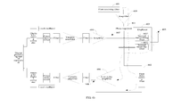
- an interference cancellation apparatus provided in another embodiment of the present invention includes a divider 301, a first 90° combiner 302, a first duplexer 303, a second duplexer 304, and a second 90° combiner 305.
- the first duplexer 303 and the second duplexer 304 are connected with the second 90° combiner 305, and the second 90° combiner 305 is connected with the antenna 306.
- the first duplexer 303 and the second duplexer 304 may be integrated on the same substrate such as a silicon wafer semiconductor substrate; the first duplexer 303 and the second duplexer 304 that are integrated on the same substrate may be an FBAR or SAW, or may be a BAW; the first duplexer 303 includes a first receiving filter 3031 and a first transmitting filter 3032, and the second duplexer 304 includes a second receiving filter 3041 and a second transmitting filter 3042; and the symmetry between the first duplexer 303 and the second duplexer 304 includes symmetry between the first transmitting filter 3032 and the second transmitting filter 3042, or includes symmetry between the first transmitting filter 3032 and the second transmitting filter 3042, and symmetry between the first receiving filter 3031 and the second receiving filter 3041.
- symmetry between the first transmitting filter and the second transmitting filter refers to consistent electric performance between the first transmitting filter and the second transmitting filter
- symmetry between the first receiving filter and the second receiving filter refers to consistent electric performance between the first receiving filter and the second receiving filter.
- consistent electric performance include: The electric performance is completely the same, or, the impact caused by the difference of the electric performance onto the interference cancellation result is in an acceptable range.
- the electric performance may include transmission response delay, phase, amplitude, and so on.
- the structure and features being the same is one of the scenarios of consistent electric performance. That is, symmetry scenarios include the scenario of the structure and features being the same.
- the transmitted signal passes through the devices such as digital processing unit of the transceiver, digital-to-analog converter, frequency mixer, filter 307, and amplifier, and enters the divider 301.
- the transmitted signal is divided into two signals with a phase difference of 90°, for example, a first transmitted signal whose phase is 90° (or 0°) and a second transmitted signal whose phase is 180° (or 90°).
- Each transmitted signal includes not only the transmitted signal itself, but also an intermodulation signal.
- the intermodulation signal is derived from the transmitted signal due to nonlinearity of the devices such as the amplifier 307.
- the first transmitted signal is input into the first duplexer 303, and the second transmitted signal is input into the second duplexer 304.
- the first transmitting signal is input into the first duplexer 303, although a majority of the signal passes through the first transmitting filter 3032 and is input to the second 90° combiner 305 connected with the first duplexer 303, a part of the signal (including a part of the first transmitted signal and the intermodulation signal derived from the first transmitted signal) still passes through the first receiving filter 3031 and the first 90° combiner 302, and leaks to the receiving channel.
- Such signals are the first interfering signal that travels along the following route:
- the signal is output from the first transmitting filter 3032 to the first receiving filter 3031, and then output from the first receiving filter 3031 to the first 90° combiner 302.
- the dotted line in FIG. 3 shows the route of the interfering signal.
- the second transmitting signal is input into the second duplexer 304, although a majority of the signal passes through the second transmitting filter 3042 in the second duplexer and is input to the second 90° combiner 305 connected with the second duplexer 304, a part of the signal (including a part of the second transmitted signal and the intermodulation signal derived from the second transmitted signal) still passes through the second receiving filter 3041 and the first 90° combiner 302, and leaks to the receiving channel.
- Such signals are the second interfering signal that travels along the following route: The signal is output from the second transmitting filter 3042 to the second receiving filter 3041, and then output from the second receiving filter 3041 to the first 90° combiner 302.
- the dotted line in FIG. 3 shows the route of the interfering signal. If the interfering signal leaked to the receiving channel is not cancelled, the interfering signal will cause interference to the received signal transmitted from the first receiving filter 3031 and the second receiving filter 3041.
- the second 90° combiner 305 performs 90° combination for the first transmitted signal output by the first transmitting filter 3032 and the second transmitted signal output by the second transmitting filter 3042, and then outputs the combined signal from the antenna 306 connected with the combiner. In this way, the power or energy of the transmitted signal suffers little loss.
- the second 90° combiner 305 performs 90° division for the received signal, and inputs the divided signals to the first duplexer 303 and the second duplexer 304 respectively. Due to the filtering effect of the first transmitting filter 3032 and the second transmitting filter 3042 (the stopband of the transmitting filter overlaps the passband of the receiving filter), the received signal output from the second 90° combiner 305 is input from the first receiving filter 3031 and the second receiving filter 3041 respectively, and then output from the first 90° combiner 302 to the receiving channel, instead of being input from the first transmitting filter 3032 and the second transmitting filter 3042 and then output from the first 90° combiner 302 to the transmitting channel.
- the first interfering signal output from the first receiving filter 3031 and the second interfering signal output from the second receiving filter 3041 undergo 90° phase shift at the 90° combiner 302 and are input to a low noise amplifier 307.
- the first transmitting filter 3032 is symmetric to the second transmitting filter 3042, and the difference between the phase of the first transmitted signal and the phase of the second transmitted signal is 90° after the signals pass through the divider 301. Therefore, after the 90° combiner 302 performs 90° phase shift for the part of the first transmitted signal output from the first receiving filter 3031 and the part of the second transmitted signal output from the second receiving filter 3041, and before the signals are input to the low noise amplifier 307, the phase difference is 180°, namely, the two have opposite phases.
- the two signals are cancelled or basically cancelled when being combined at the 90° combiner 302, and no interference is caused to the received signal on the receiving channel. Due to the outband filter feature of the transmitting filter, the transmitting filter is unable to filter out outband signals completely.
- the intermodulation signal output from the first receiving filter 3031, derived from the first transmitted signal, and occupying a band that overlaps the receiving band (namely, the band occupied by the received signal) is compared with the intermodulation signal output from the second receiving filter 3041, derived from the second transmitted signal, and occupying a band that overlaps the receiving band, and the comparison shows that the phase difference between the two intermodulation signals is 90°. Therefore, after the 90° combiner 302 performs 90° phase shift for the two intermodulation signals, the final phase difference is 180°, namely, the two have opposite phases.
- the first receiving filter 3031 may also be symmetric to the second receiving filter 3041. In this way, the inconsistency of the outband filter feature of the receiving filter is overcome, and the effect of interference cancellation is strengthened.
- the relationship between the part of the first transmitted signal output from the first receiving filter 3031 of the first duplexer 303 and the part of the second transmitted signal output from the second receiving filter 3041 of the second duplexer 304 is similar to the relationship applicable when the first transmitting filter 3032 is symmetric to the second transmitting filter 3042, namely, after the 90° combiner 302 performs 90° phase shift, the final phase difference is 180°, namely, the two have opposite phases.
- the intermodulation signal output from the first receiving filter 3031, derived from the first transmitted signal, and occupying a band that overlaps the transmitting band (and/or overlaps no receiving band) is compared with the intermodulation signal output from the second receiving filter 3041, derived from the second transmitted signal, and occupying a band that overlaps the transmitting band and/or overlaps no receiving band, and the comparison shows that the phase difference between the two intermodulation signals is 90°. Therefore, after the 90° combiner 302 performs 90° phase shift for the two intermodulation signals, the final phase difference is 180°, namely, the two have opposite phases.
- the signal dividing module 201 shown in FIG. 2 may be a coupler or includes a coupler; the phasing module 202 is specifically a phase regulator or includes a phase regulator.
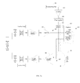
- an interference cancellation apparatus provided in another embodiment of the present invention includes a first receiving filter 401, a first transmitting filter 402, a duplexer 403, a phase regulator 404, a first coupler 407, a second coupler 408, an amplifier 409 and so on.
- the duplexer 403 is connected with the antenna 405, and the first transmitting filter 402 is not connected with the antenna 405.
- the duplexer 403 includes a second receiving filter 4031 and a second transmitting filter 4032.
- the first receiving filter 401, the first transmitting filter 402, and the duplexer 403 may be integrated on the same substrate such as a silicon wafer semiconductor substrate; the first receiving filter 401, the first transmitting filter 402, and the duplexer 403 integrated on the same substrate may be an FBAR or SAW, or may be a BAW.
- the first transmitting filter 402 is symmetric to the second transmitting filter 4032 of the duplexer 403; or, the first transmitting filter 402 is symmetric to the second transmitting filter 4032 of the duplexer 403, and the first receiving filter 401 is symmetric to the second receiving filter 4031 of the duplexer 403.
- symmetry or "symmetric" see the definition above.
- symmetry between the first transmitting filter and the second transmitting filter of the duplexer refers to consistent electric performance between the first transmitting filter and the second transmitting filter of the duplexer
- symmetry between the first receiving filter and the second receiving filter of the duplexer refers to consistent electric performance between the first receiving filter and the second receiving filter of the duplexer.
- the meanings of "consistent electric performance” include: The electric performance is completely the same, or, the impact caused by the difference of the electric performance onto the interference cancellation result is in an acceptable range.
- the electric performance may include transmission response delay, phase, amplitude, and so on.
- the structure and features being the same is one of the scenarios of consistent electric performance. That is, symmetry scenarios include the scenario of the structure and features being the same.
- the first coupler 407 couples a part of the transmitted signal out of the amplifier, and inputs the signal as a first transmitted signal into the first receiving filter 401; the first receiving filter 401 filters the first transmitted signal and inputs it into the phase regulator 404; finally, the phase regulator 404 performs 180° phase regulation for the signal, and inputs the signal into the first transmitting filter 402.
- the first transmitted signal is filtered by the first receiving filter 401, a part of the first transmitted signal and the intermodulation signal derived from the first transmitted signal are still not filtered out by the first receiving filter 401. Such signals that are not filtered out make up the first interfering signal.
- the first interfering signal is output from the first receiving filter 401 to the phase regulator 404, and then input into the first transmitting filter 402, and finally output from the first transmitting filter 402.
- the dotted line in FIG. 4a shows the route of the leaked interfering signal.
- the part not coupled by the first coupler 407 in the transmitted signal namely, the transmitted signal not coupled by the first coupler 407, is output as a second transmitted signal to the duplexer 403.
- the second transmitting filter 4032 in the duplexer 403 can transmit a majority of the second transmitted signal to the antenna 405 and then the antenna 405 transmits the signal, a part of the second transmitted signal and the intermodulation signal derived from the second transmitted signal are still not filtered out by the second receiving filter 4031 and are leaked to the receiving channel.
- Such signals that are not filtered out make up the second interfering signal.
- the second interfering signal is output from the second receiving filter 4031 to the second transmitting filter 4032, and finally output from the second transmitting filter 4032.
- the dotted line in FIG. 4a shows the route of the leaked interfering signal.
- the interference cancellation apparatus shown in FIG. 4a after the transmitted signal is output from the amplifier 410, a majority of the transmitted signal is input to the second transmitting filter 4032 of the duplexer, and the coupler 407 couples only a very small part of the transmitted signal and inputs it to the first receiving filter 401.
- the first transmitted signal output from the first receiving filter 401 is coupled by the coupler, and its power or energy is small; the power or energy of the second transmitted signal output by the second transmitting filter 4032 is far greater than the power or energy of the first transmitted signal. Therefore, even if no cancellation apparatus shown in FIG. 3 combines the second transmitted signal output by the second transmitting filter 4032 with the first transmitted signal output by the first transmitting filter 402, the power or energy of the transmitted signal output by the amplifier 410 suffers no great loss, or the lost energy or power is ignorable.
- the received signal is input from the second receiving filter 4031 and then output by the low noise amplifier 406 to the receiving channel, instead of being input from the second transmitting filter 4032 and then output by the amplifier 410 to the transmitting channel.
- the first interfering signal undergoes 180° phase shift performed by the phase regulator 404, and is then input to the first transmitting filter 402.
- the first transmitting filter 402 is symmetric to the second transmitting filter 4032, and the phase of the signal output from the first transmitting filter 402 is the same as the phase of the first transmitted signal output by the phase regulator 404 after the 180° phase shift, and therefore, the phase difference between the part of the first transmitted signal output from the first transmitting filter 402 and the part of the second transmitted signal output from the second receiving filter 4031 is 180°, namely, the two have opposite phases. Due to the outband filter feature of the transmitting filter, the transmitting filter is unable to filter out outband signals completely.
- the phase of the intermodulation signal which is output from the first transmitting filter 402, derived from the first transmitted signal, and occupying a band that overlaps the receiving band (namely, the band occupied by the received signal), is the same as the phase of the intermodulation signal output by the phase regulator 404 after the 180° phase shift. Therefore, the intermodulation signal output from the first transmitting filter 402, derived from the first transmitted signal, and occupying a band that overlaps the receiving band is compared with the intermodulation signal output from the second receiving filter 4031, derived from the second transmitted signal, and occupying a band that overlaps the receiving band, and the comparison shows that the phase difference is 180°, namely, the two have opposite phases.
- the first receiving filter 401 may also be symmetric to the second receiving filter 4041. In this way, the inconsistency of the outband filter feature of the receiving filter is overcome, and the effect of interference cancellation is strengthened.
- the relationship between the part of the first transmitted signal output from the first transmitting filter 402 and the part of the second transmitted signal output from the second receiving filter 4031 is similar to the relationship applicable when the first transmitting filter 402 is symmetric to the second transmitting filter 4032, namely, after the phase regulator performs the 180° phase shift, the final phase difference is 180°, namely, the two have opposite phases.
- the phase of the intermodulation signal which is output from the first transmitting filter 402, derived from the first transmitted signal, and occupying a band that overlaps the transmitting band (and/or overlaps no receiving band), is the same as the phase of the intermodulation signal output after the signal undergoes the 180° phase shift performed by the phase regulator.
- the intermodulation signal output from the first transmitting filter 402, derived from the first transmitted signal, and occupying a band that overlaps the transmitting band (and/or overlaps no receiving band) is compared with the intermodulation signal output from the second receiving filter 4031, derived from the second transmitted signal, and occupying a band that overlaps the transmitting band (and/or overlaps no receiving band), and the comparison shows that the phase difference is 180°, namely, the two have opposite phases.
- the second interfering signal output by the second receiving filter 4031 and the first interfering signal coupled by the second coupler 408 from the first transmitting filter 402 are input into the low noise amplifier 406, and then the low noise amplifier 406 overlay the signals directly, thereby the signals of opposite phases are combined.
- the second interfering signal output by the second receiving filter 4031 is input into the low noise amplifier 406, and then the signal is output by the low noise amplifier 406 and coupled by the second coupler 408 with the first interfering signal output from the first transmitting filter 402, thereby the signals of opposite phases are combined.
- Combining the signals of opposite phases means that the two signals are cancelled or basically cancelled, and no interference is caused to the received signal on the receiving channel, namely, the suppression performed by the transmitting side for the receiving side is reduced.
- the amplitude of the first interfering signal may be adjusted before, when, or after the first interfering signal output from the first receiving filter 401 is input into the phase regulator 404 for undergoing the 180° phase shift. Specifically, the amplitude of the first interfering signal is adjusted as equal to the amplitude of the second interfering signal. That is, the phasing module 202 shown in FIG. 2 may be an amplitude phase regulator, which includes an amplitude regulator 501.
- FIG. 5a or FIG. 5b shows an interference cancellation apparatus provided in another embodiment of the present invention.
- the amplitude regulator 501 is connected with the phase regulator 404 or the first receiving filter 401, and is configured to adjust the amplitude of the first interfering signal so that the amplitude of the first interfering signal is equal to the amplitude of the second interfering signal. In this way, after the phase regulator 404 performs the 180° phase shift for the first interfering signal, if the first interfering signal is combined with the second interfering signal, the two interfering signals are completely cancelled.
- the phasing module 202 includes a phase adjusting unit 601 and an amplitude adjusting unit 602, as shown in the interference cancellation apparatus in FIG. 6a or FIG. 6b .
- the phase adjusting unit 601 is configured to perform 180° phase shift for the first interfering signal output by the first receiving filter 401, and then input the signal to the amplitude adjusting unit 602.
- the amplitude adjusting unit 602 is configured to adjust the amplitude of the first interfering signal so that the amplitude of the first interfering signal is equal to the amplitude of the second interfering signal.
- the amplitude adjusting unit 602 inputs the first interfering signal that has undergone amplitude adjustment into the first transmitting filter 402; or the amplitude adjusting unit 602 is configured to adjust the amplitude of the first interfering signal output by the first receiving filter 401 so that the amplitude of the first interfering signal is equal to the amplitude of the second interfering signal output by the second receiving filter 402.
- the amplitude adjusting unit 602 outputs the first interfering signal that has undergone amplitude adjustment to the phase adjusting unit 601, and then the phase adjusting unit 601 performs 180° phase shift for the first interfering signal output by the amplitude adjusting unit 602 and inputs the signal to the first transmitting filter 402. In this way, the first interfering signal and the second interfering signal are completely cancelled after the two interfering signals of equal amplitudes and opposite phases are combined.
- a base station is provided in an embodiment of the present invention.
- the base station may include the interference cancellation apparatus provided in any embodiment shown in FIG. 2 to FIG. 6b .
- a communication system is provided in an embodiment of the present invention, for example, an FDM system.
- the communication system may include the base station provided in an embodiment of the present invention.
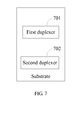
- FIG. 7 is a schematic structural diagram of a filter (filter device) according to an embodiment of the present invention. For ease of description, only the part related to this embodiment of the present invention is illustrated.
- the filter shown in FIG. 7 includes a first duplexer 701 and a second duplexer 702 symmetric to the first duplexer 701.
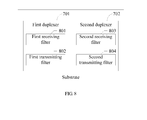
- FIG. 8 shows a filter provided in another embodiment of the present invention.
- the first duplexer shown in FIG. 7 further includes a first receiving filter 801 and a first transmitting filter 802.
- the second duplexer 702 includes a second receiving filter 803 and a second transmitting filter 804.
- the first transmitting filter 802 is symmetric to the second transmitting filter 804; or, the first receiving filter 801 is symmetric to the second receiving filter 803 and the first transmitting filter 802 is symmetric to the second transmitting filter 804.
- symmetry between the first transmitting filter and the second transmitting filter refers to consistent electric performance between the first transmitting filter and the second transmitting filter
- symmetry between the first receiving filter and the second receiving filter refers to consistent electric performance between the first receiving filter and the second receiving filter.
- the meanings of "consistent electric performance” include: The electric performance is completely the same, or, the impact caused by the difference of the electric performance onto the interference cancellation result is in an acceptable range.
- the electric performance may include transmission response delay, phase, amplitude, and so on.
- the structure and features being the same is one of the scenarios of consistent electric performance. That is, symmetry scenarios include the scenario of the structure and features being the same.
- the first duplexer 701 and the second duplexer 702 shown in FIG. 7 or FIG. 8 may be integrated on the same substrate such as a silicon wafer semiconductor substrate.
- the first duplexer and the second duplexer may also be integrated on the same chip (die or chip), or integrated in the same package (package), or integrated in the same module (module) so as to accomplish consistent electric performance between the first transmitting filter of the first duplexer and the second transmitting filter of the second duplexer, or, further, accomplish consistent electric performance between the first receiving filter of the first duplexer and the second receiving filter of the second duplexer.
- the first transmitting filter and the second transmitting filter are integrated on the same substrate.
- the same temperature feature also aims to accomplish better symmetry of the filters, namely, accomplish better consistency of electric performance between the first transmitting filter and the second transmitting filter, or, further, accomplish better consistency of electric performance between the first receiving filter and the second receiving filter.
- the first transmitting filter and the second transmitting filter are integrated on the same chip, or integrated on the same substrate, or integrated in the same package, or integrated in the same module.
- FIG. 9 is a schematic structural diagram of filter (filter device) according to an embodiment of the present invention.
- the filter shown in FIG. 9 includes a first receiving filter 901, a first transmitting filter 902, and a duplexer 903.
- the duplexer 903 includes a second receiving filter 9031 and a second transmitting filter 9032, where the first transmitting filter 902 is symmetric to the second transmitting filter 9032; or, the first receiving filter 901 is symmetric to the second receiving filter 9031 and the first transmitting filter 902 is symmetric to the second transmitting filter 9032.
- symmetry or "symmetric" see the definition above.
- symmetry between the first transmitting filter and the second transmitting filter refers to consistent electric performance between the first transmitting filter and the second transmitting filter
- symmetry between the first receiving filter and the second receiving filter refers to consistent electric performance between the first receiving filter and the second receiving filter.
- the meanings of "consistent electric performance” include: The electric performance is completely the same, or, the impact caused by the difference of the electric performance onto the interference cancellation result is in an acceptable range.
- the electric performance may include transmission response delay, phase, amplitude, and so on.
- the structure and features being the same is one of the scenarios of consistent electric performance. That is, symmetry scenarios include the scenario of the structure and features being the same.
- the first receiving filter 901, the first transmitting filter 902, and the duplexer 903 shown in FIG. 9 may be integrated on the same substrate such as a silicon wafer semiconductor substrate.
- the symmetry between the first receiving filter, the first transmitting filter, and the duplexer inclusive of the second receiving filter and the second transmitting filter may also be integrated on the same chip (die or chip), or integrated in the same package (package), or integrated in the same module (module) so as to accomplish consistent electric performance between the first transmitting filter and the second transmitting filter in the duplexer, or, further, accomplish consistent electric performance between the first receiving filter and the second receiving filter in the duplexer.
- the first transmitting filter and the second transmitting filter are integrated on the same substrate. Understandably, "keep the same temperature feature" mentioned above also aims to accomplish better symmetry of the filters, namely, accomplish better consistency of electric performance between the first transmitting filter and the second transmitting filter in the duplexer, or, further, accomplish better consistency of electric performance between the first receiving filter and the second receiving filter in the duplexer.
- the second transmitting filter of the duplexer and the first transmitting filter are integrated on the same chip, or integrated on the same substrate, or integrated in the same package, or integrated in the same module.
- a filter device in an embodiment of the present invention.
- the filter device includes a first transmitting filter and a second transmitting filter, where the first transmitting filter is symmetric to the second transmitting filter.
- the first transmitting filter and the second transmitting filter may be integrated on the same chip (die or chip), or integrated on the same substrate (substrate), or integrated in the same package (package), or integrated in the same module (module), so as to accomplish consistent electric performance between the first transmitting filter and the second transmitting filter.
- a filter device in an embodiment of the present invention.
- the filter device includes a first receiving filter and a second receiving filter, where the first receiving filter is symmetric to the second receiving filter.
- the first receiving filter and the second receiving filter may be integrated on the same chip (die or chip), or integrated on the same substrate (substrate), or integrated in the same package (package), or integrated in the same module (module), so as to accomplish consistent electric performance between the first receiving filter and the second receiving filter.
- the filter device includes a first transmitting filter and a second transmitting filter.
- the first transmitting filter and the second transmitting filter are integrated on the same chip, or integrated on the same substrate, or integrated in the same package, or integrated in the same module.
- the filter device includes a first receiving filter and a second receiving filter.
- the first receiving filter and the second receiving filter are integrated on the same chip, or integrated on the same substrate, or integrated in the same package, or integrated in the same module.
- the filter device includes a first duplexer and a second duplexer.
- the first duplexer and the second duplexer are integrated on the same chip, or integrated on the same substrate, or integrated in the same package, or integrated in the same module.
- the filter device includes a first receiving filter, a first transmitting filter, and a duplexer.
- the duplexer, the first receiving filter, and the first transmitting filter are integrated on the same chip, or integrated on the same substrate, or integrated in the same package, or integrated in the same module.
- a transmitted signal refers to a signal output from a digital processing unit of a transceiver, processed by the modules such as digital-to-analog converter, frequency mixer, filter, and amplifier on the transmitting channel, and to be transmitted from antenna port; and a received signal refers to a signal received from the antenna port, to be processed by the modules such as amplifier, filter, frequency mixer, and analog-to-digital converter on the transmitting channel, and to be input into the digital processing unit of the transceiver.
- the transmitted signal in the embodiments of the present invention is not limited to the transmitted signal at the antenna port, but may be the signal at any position in the transmitting channel, for example, the signal before the amplifier.
- the first transmitted signal may pass the same devices as those passed by the transmitted signal not coupled (the second transmitted signal), namely, flows along the same route. In this way, although more devices need to be added to cancel interference, the similar effect is accomplished. However, considering the cost, if a device is not very influential in processing signals or accomplishing a better effect of interference cancellation, the device may be omitted in the route existent before the first transmitted signal is input into the first transmitting filter. Besides, the location of combining two interfering signals is not limited to the antenna port described in the embodiments above, but may be any position in the receiving channel.
- the coupled transmitted signal (the first transmitted signal) is output from a interference cancellation filtering unit (such as the first duplexer, or the first receiving filter and the first transmitting filter) (the output signal is the first interfering signal)
- the first interfering signal is processed by the same devices in the receiving channel as those that handle the transmitted signal not coupled (the second transmitted signal) and output by the second duplexer (the output signal is the second interfering signal), and then the two interfering signals are combined.
- the cost if a device is not very influential in processing signals or accomplishing a better effect of interference cancellation, the device may be omitted in the route existent before the first interfering signal and the second interfering signal are combined. Such variations do not affect implementation or protection of the present invention.
- the first interfering signal includes a signal leaked from the first transmitted signal to a receiving channel after the first transmitted signal flows through the first transmitting filter and a first receiving filter
- the second interfering signal includes a signal leaked from the second transmitted signal to the receiving channel after the second transmitted signal flows through the second transmitting filter and a second receiving filter
- the receiving channel is a channel for a receiver to receive signals
- the program may be stored in a computer readable storage medium, and the storage medium may be a read-only memory (ROM, Read Only Memory), random access memory (RAM, Random Access Memory), magnetic disk, CD-ROM, and so on.
- ROM Read Only Memory
- RAM Random Access Memory
- magnetic disk CD-ROM
Landscapes
- Engineering & Computer Science (AREA)
- Signal Processing (AREA)
- Computer Networks & Wireless Communication (AREA)
- Transceivers (AREA)
- Noise Elimination (AREA)
Applications Claiming Priority (2)
| Application Number | Priority Date | Filing Date | Title |
|---|---|---|---|
| CN201210019762.7A CN102571655B (zh) | 2012-01-21 | 2012-01-21 | 一种干扰对消的方法、装置和一种滤波器 |
| PCT/CN2012/071192 WO2013107067A1 (fr) | 2012-01-21 | 2012-02-16 | Procédé et dispositif d'annulation de brouillage et dispositif de filtrage |
Publications (3)
| Publication Number | Publication Date |
|---|---|
| EP2802081A1 true EP2802081A1 (fr) | 2014-11-12 |
| EP2802081A4 EP2802081A4 (fr) | 2015-01-14 |
| EP2802081B1 EP2802081B1 (fr) | 2019-07-31 |
Family
ID=46416149
Family Applications (1)
| Application Number | Title | Priority Date | Filing Date |
|---|---|---|---|
| EP12865951.3A Active EP2802081B1 (fr) | 2012-01-21 | 2012-02-16 | Procédé et dispositif d'annulation de brouillage et dispositif de filtrage |
Country Status (6)
| Country | Link |
|---|---|
| US (1) | US9544125B2 (fr) |
| EP (1) | EP2802081B1 (fr) |
| JP (1) | JP5888630B2 (fr) |
| KR (1) | KR101594451B1 (fr) |
| CN (1) | CN102571655B (fr) |
| WO (1) | WO2013107067A1 (fr) |
Cited By (1)
| Publication number | Priority date | Publication date | Assignee | Title |
|---|---|---|---|---|
| WO2016191992A1 (fr) * | 2015-05-30 | 2016-12-08 | 华为技术有限公司 | Dispositif et procédé d'annulation de signal brouilleur |
Families Citing this family (30)
| Publication number | Priority date | Publication date | Assignee | Title |
|---|---|---|---|---|
| CN102811069B (zh) * | 2012-07-25 | 2014-10-08 | 华为技术有限公司 | 一种收发信机和干扰对消方法 |
| EP2733781A1 (fr) | 2012-11-16 | 2014-05-21 | Alcatel-Lucent | Ensemble filtre et procédé de filtrage |
| WO2014085345A1 (fr) * | 2012-11-30 | 2014-06-05 | P-Wave Holdings, Llc | Détecteur d'intermodulation passive intégré pour équipement de station de base |
| CN105099972B (zh) * | 2012-12-11 | 2018-05-04 | 华为技术有限公司 | 发射机的发射通道间干扰消除方法及装置 |
| WO2014202121A1 (fr) * | 2013-06-18 | 2014-12-24 | Telefonaktiebolaget L M Ericsson (Publ) | Unité en duplex |
| WO2015135197A1 (fr) * | 2014-03-14 | 2015-09-17 | 华为技术有限公司 | Dispositif et procédé d'élimination d'interférence |
| CN104506209B (zh) * | 2014-12-15 | 2017-02-22 | 北京邮电大学 | 一种基于耦合线紧耦合器的全双工自干扰信号消除方法和系统 |
| CN108352853B (zh) | 2015-11-04 | 2020-07-31 | 株式会社村田制作所 | 分波装置及其设计方法 |
| CN105812003B (zh) * | 2016-03-21 | 2019-02-05 | Oppo广东移动通信有限公司 | 杂散干扰抑制方法、杂散干扰抑制装置及电子装置 |
| CN106299691B (zh) * | 2016-08-09 | 2019-03-15 | 中国舰船研究设计中心 | 具有两级对消功能的收发天线共址耦合干扰抑制装置 |
| JP2018050159A (ja) * | 2016-09-21 | 2018-03-29 | 株式会社村田製作所 | 送受信モジュール |
| CN106936468B (zh) * | 2017-03-02 | 2020-03-03 | 北京小米移动软件有限公司 | 信号处理方法及装置 |
| JP2020512770A (ja) * | 2017-03-27 | 2020-04-23 | クム ネットワークス, インコーポレイテッドKumu Networks, Inc. | 調整可能な帯域外干渉緩和システムおよび方法 |
| CN108964679B (zh) * | 2017-05-18 | 2021-09-28 | 中兴通讯股份有限公司 | 功率容量提升方法、装置和设备 |
| CN107271769A (zh) * | 2017-06-19 | 2017-10-20 | 电子科技大学 | 基波对消技术无源互调测试系统及其测试方法 |
| CN107529623B (zh) * | 2017-09-29 | 2025-05-02 | 珠海微度芯创科技有限责任公司 | 一种提高收发隔离度的天线馈电网络系统 |
| CN108023608B (zh) | 2017-12-04 | 2020-03-06 | 中兴通讯股份有限公司 | 全时双工系统、电路、终端、控制方法及可读介质 |
| US11271660B2 (en) * | 2018-05-17 | 2022-03-08 | Institut National De La Recherche Scientifique | Method and system for sampling and denoising amplification of a signal |
| CN112236946A (zh) * | 2018-06-04 | 2021-01-15 | 株式会社村田制作所 | 高频前端模块和通信装置 |
| CN109085540B (zh) * | 2018-09-06 | 2021-02-02 | 杭州捍鹰科技有限公司 | 泄漏信号的对消处理方法、装置及系统 |
| CN109743067A (zh) * | 2019-03-21 | 2019-05-10 | 惠州Tcl移动通信有限公司 | 干扰消除设备和干扰消除方法 |
| US10749565B1 (en) * | 2019-04-30 | 2020-08-18 | T-Mobile Usa, Inc. | RF front end reduction of receiver de-sensitivity |
| CN112398494B (zh) * | 2019-08-16 | 2023-07-04 | 中兴通讯股份有限公司 | 路由器及其干扰消除装置、方法、及存储介质 |
| CN110649930B (zh) * | 2019-10-09 | 2021-06-22 | 河南理工大学 | 大规模天线中本振泄露的抑制方法及系统 |
| CN111832327A (zh) * | 2020-07-15 | 2020-10-27 | 南方科技大学 | 一种rfid读写器载波抑制方法 |
| CN114070339B (zh) * | 2020-07-31 | 2023-06-20 | 华为技术有限公司 | 同频收发器共存装置、方法以及计算机存储介质 |
| CN112421224B (zh) * | 2020-09-28 | 2023-11-17 | 广东盛路通信科技股份有限公司 | 基于蓝牙通信和5g网络通信的天线及其控制方法 |
| JP2022076338A (ja) * | 2020-11-09 | 2022-05-19 | 株式会社村田製作所 | 高周波信号送受信回路 |
| CN114696868B (zh) * | 2020-12-30 | 2025-09-12 | 中兴通讯股份有限公司 | 降低nr和wifi干扰的方法、装置、设备和存储介质 |
| US12250010B2 (en) | 2021-04-07 | 2025-03-11 | Skyworks Solutions, Inc. | Systems and methods for diplexer circuits with leakage cancellation |
Family Cites Families (13)
| Publication number | Priority date | Publication date | Assignee | Title |
|---|---|---|---|---|
| BR9917191A (pt) * | 1999-03-03 | 2001-12-26 | Siemens Ag | Transmissor-receptor por divisão de frequência eprocesso para eliminação de diafonia |
| CA2413714C (fr) * | 2001-12-07 | 2011-11-15 | Ecole De Technologie Superieure | Duplexeur electronique reglable |
| KR101047731B1 (ko) * | 2003-09-01 | 2011-07-08 | 엘지이노텍 주식회사 | 듀플렉서 회로 |
| CN2826837Y (zh) * | 2005-03-10 | 2006-10-11 | 台扬科技股份有限公司 | 同载波频率收发传输路径的隔离电路 |
| US8364092B2 (en) * | 2005-04-14 | 2013-01-29 | Ecole De Technologie Superieure | Balanced active and passive duplexers |
| JP4735551B2 (ja) * | 2007-01-19 | 2011-07-27 | 日立電線株式会社 | 通信基地局及びそれを用いた通信システム |
| US8004538B2 (en) | 2007-09-21 | 2011-08-23 | Global Oled Technology Llc | Preferential tone scale for electronic displays |
| JP5629774B2 (ja) * | 2009-09-21 | 2014-11-26 | ケーエムダブリュ・インコーポレーテッド | 無線通信基地局の共用化装置 |
| CN101888252B (zh) * | 2010-04-20 | 2013-04-10 | 宁波成电泰克电子信息技术发展有限公司 | 一种提高rf系统中动态范围的方法及系统 |
| CN101834625B (zh) * | 2010-04-23 | 2012-03-21 | 华为技术有限公司 | 射频信号环回方法及室外单元 |
| JP2012138651A (ja) | 2010-12-24 | 2012-07-19 | Hitachi Media Electoronics Co Ltd | 移動通信端末用モジュール、及び移動通信端末 |
| EP2512040B1 (fr) * | 2011-04-14 | 2013-11-13 | Alcatel Lucent | Annuleur d'écho enregistrant les calculs pour signal audio de bande large |
| CN102231638A (zh) * | 2011-06-02 | 2011-11-02 | 苏州易特诺科技股份有限公司 | 一种多系统共天/馈线模块及其基站 |
-
2012
- 2012-01-21 CN CN201210019762.7A patent/CN102571655B/zh not_active Expired - Fee Related
- 2012-02-16 JP JP2014552472A patent/JP5888630B2/ja active Active
- 2012-02-16 KR KR1020147023379A patent/KR101594451B1/ko active Active
- 2012-02-16 EP EP12865951.3A patent/EP2802081B1/fr active Active
- 2012-02-16 WO PCT/CN2012/071192 patent/WO2013107067A1/fr not_active Ceased
-
2014
- 2014-07-21 US US14/336,709 patent/US9544125B2/en active Active
Cited By (2)
| Publication number | Priority date | Publication date | Assignee | Title |
|---|---|---|---|---|
| WO2016191992A1 (fr) * | 2015-05-30 | 2016-12-08 | 华为技术有限公司 | Dispositif et procédé d'annulation de signal brouilleur |
| US10033417B2 (en) | 2015-05-30 | 2018-07-24 | Huawei Technologies Co., Ltd. | Interference signal cancellation apparatus and method |
Also Published As
| Publication number | Publication date |
|---|---|
| EP2802081A4 (fr) | 2015-01-14 |
| JP5888630B2 (ja) | 2016-03-22 |
| KR101594451B1 (ko) | 2016-02-16 |
| US20140328222A1 (en) | 2014-11-06 |
| JP2015504283A (ja) | 2015-02-05 |
| CN102571655A (zh) | 2012-07-11 |
| EP2802081B1 (fr) | 2019-07-31 |
| KR20140114890A (ko) | 2014-09-29 |
| US9544125B2 (en) | 2017-01-10 |
| CN102571655B (zh) | 2014-12-17 |
| WO2013107067A1 (fr) | 2013-07-25 |
Similar Documents
| Publication | Publication Date | Title |
|---|---|---|
| US9544125B2 (en) | Interference cancellation method and apparatus, filter device | |
| US10979021B2 (en) | System and method for a radio frequency filter | |
| US9455756B2 (en) | Systems and methods for frequency independent analog self-interference cancellation | |
| US8971219B2 (en) | Hybrid transformer based integrated duplexer for multi-band/multi-mode radio frequency (RF) front end | |
| US10581650B2 (en) | Enhancing isolation in radio frequency multiplexers | |
| US20180138927A1 (en) | Front-end module | |
| CN103460611B (zh) | 高频前端电路 | |
| WO2016017104A1 (fr) | Filtres à ondes acoustiques et duplexeurs utilisant lesdits filtres | |
| US20140376419A1 (en) | Passive leakage cancellation networks for duplexers and coexisting wireless communication systems | |
| CN106301516B (zh) | 一种分集接收机及终端 | |
| CN110113063B (zh) | 一种射频前端电路及终端设备 | |
| CN211830764U (zh) | 一种射频电路及电子设备 | |
| KR20130121493A (ko) | 송수신 신호를 분리하는 고주파 전단장치 | |
| US20250260387A1 (en) | Acoustic filter assembly with tunable passband, a radio frequency module, and mobile device including the same | |
| EP2651039A1 (fr) | Agencement émetteur-récepteur sans duplexeur, dispositif de communication et procédé de commande | |
| WO2014157330A1 (fr) | Système de communication sans fil |
Legal Events
| Date | Code | Title | Description |
|---|---|---|---|
| PUAI | Public reference made under article 153(3) epc to a published international application that has entered the european phase |
Free format text: ORIGINAL CODE: 0009012 |
|
| 17P | Request for examination filed |
Effective date: 20140804 |
|
| AK | Designated contracting states |
Kind code of ref document: A1 Designated state(s): AL AT BE BG CH CY CZ DE DK EE ES FI FR GB GR HR HU IE IS IT LI LT LU LV MC MK MT NL NO PL PT RO RS SE SI SK SM TR |
|
| A4 | Supplementary search report drawn up and despatched |
Effective date: 20141212 |
|
| RIC1 | Information provided on ipc code assigned before grant |
Ipc: H04B 1/10 20060101AFI20141208BHEP |
|
| DAX | Request for extension of the european patent (deleted) | ||
| 17Q | First examination report despatched |
Effective date: 20161010 |
|
| STAA | Information on the status of an ep patent application or granted ep patent |
Free format text: STATUS: EXAMINATION IS IN PROGRESS |
|
| GRAP | Despatch of communication of intention to grant a patent |
Free format text: ORIGINAL CODE: EPIDOSNIGR1 |
|
| STAA | Information on the status of an ep patent application or granted ep patent |
Free format text: STATUS: GRANT OF PATENT IS INTENDED |
|
| INTG | Intention to grant announced |
Effective date: 20190213 |
|
| GRAS | Grant fee paid |
Free format text: ORIGINAL CODE: EPIDOSNIGR3 |
|
| GRAA | (expected) grant |
Free format text: ORIGINAL CODE: 0009210 |
|
| STAA | Information on the status of an ep patent application or granted ep patent |
Free format text: STATUS: THE PATENT HAS BEEN GRANTED |
|
| AK | Designated contracting states |
Kind code of ref document: B1 Designated state(s): AL AT BE BG CH CY CZ DE DK EE ES FI FR GB GR HR HU IE IS IT LI LT LU LV MC MK MT NL NO PL PT RO RS SE SI SK SM TR |
|
| REG | Reference to a national code |
Ref country code: CH Ref legal event code: EP Ref country code: GB Ref legal event code: FG4D |
|
| REG | Reference to a national code |
Ref country code: DE Ref legal event code: R096 Ref document number: 602012062553 Country of ref document: DE |
|
| REG | Reference to a national code |
Ref country code: AT Ref legal event code: REF Ref document number: 1162035 Country of ref document: AT Kind code of ref document: T Effective date: 20190815 |
|
| REG | Reference to a national code |
Ref country code: IE Ref legal event code: FG4D |
|
| REG | Reference to a national code |
Ref country code: NL Ref legal event code: MP Effective date: 20190731 |
|
| REG | Reference to a national code |
Ref country code: LT Ref legal event code: MG4D |
|
| REG | Reference to a national code |
Ref country code: AT Ref legal event code: MK05 Ref document number: 1162035 Country of ref document: AT Kind code of ref document: T Effective date: 20190731 |
|
| PG25 | Lapsed in a contracting state [announced via postgrant information from national office to epo] |
Ref country code: NO Free format text: LAPSE BECAUSE OF FAILURE TO SUBMIT A TRANSLATION OF THE DESCRIPTION OR TO PAY THE FEE WITHIN THE PRESCRIBED TIME-LIMIT Effective date: 20191031 Ref country code: NL Free format text: LAPSE BECAUSE OF FAILURE TO SUBMIT A TRANSLATION OF THE DESCRIPTION OR TO PAY THE FEE WITHIN THE PRESCRIBED TIME-LIMIT Effective date: 20190731 Ref country code: SE Free format text: LAPSE BECAUSE OF FAILURE TO SUBMIT A TRANSLATION OF THE DESCRIPTION OR TO PAY THE FEE WITHIN THE PRESCRIBED TIME-LIMIT Effective date: 20190731 Ref country code: BG Free format text: LAPSE BECAUSE OF FAILURE TO SUBMIT A TRANSLATION OF THE DESCRIPTION OR TO PAY THE FEE WITHIN THE PRESCRIBED TIME-LIMIT Effective date: 20191031 Ref country code: LT Free format text: LAPSE BECAUSE OF FAILURE TO SUBMIT A TRANSLATION OF THE DESCRIPTION OR TO PAY THE FEE WITHIN THE PRESCRIBED TIME-LIMIT Effective date: 20190731 Ref country code: HR Free format text: LAPSE BECAUSE OF FAILURE TO SUBMIT A TRANSLATION OF THE DESCRIPTION OR TO PAY THE FEE WITHIN THE PRESCRIBED TIME-LIMIT Effective date: 20190731 Ref country code: FI Free format text: LAPSE BECAUSE OF FAILURE TO SUBMIT A TRANSLATION OF THE DESCRIPTION OR TO PAY THE FEE WITHIN THE PRESCRIBED TIME-LIMIT Effective date: 20190731 Ref country code: PT Free format text: LAPSE BECAUSE OF FAILURE TO SUBMIT A TRANSLATION OF THE DESCRIPTION OR TO PAY THE FEE WITHIN THE PRESCRIBED TIME-LIMIT Effective date: 20191202 Ref country code: AT Free format text: LAPSE BECAUSE OF FAILURE TO SUBMIT A TRANSLATION OF THE DESCRIPTION OR TO PAY THE FEE WITHIN THE PRESCRIBED TIME-LIMIT Effective date: 20190731 |
|
| PG25 | Lapsed in a contracting state [announced via postgrant information from national office to epo] |
Ref country code: ES Free format text: LAPSE BECAUSE OF FAILURE TO SUBMIT A TRANSLATION OF THE DESCRIPTION OR TO PAY THE FEE WITHIN THE PRESCRIBED TIME-LIMIT Effective date: 20190731 Ref country code: LV Free format text: LAPSE BECAUSE OF FAILURE TO SUBMIT A TRANSLATION OF THE DESCRIPTION OR TO PAY THE FEE WITHIN THE PRESCRIBED TIME-LIMIT Effective date: 20190731 Ref country code: GR Free format text: LAPSE BECAUSE OF FAILURE TO SUBMIT A TRANSLATION OF THE DESCRIPTION OR TO PAY THE FEE WITHIN THE PRESCRIBED TIME-LIMIT Effective date: 20191101 Ref country code: IS Free format text: LAPSE BECAUSE OF FAILURE TO SUBMIT A TRANSLATION OF THE DESCRIPTION OR TO PAY THE FEE WITHIN THE PRESCRIBED TIME-LIMIT Effective date: 20191130 Ref country code: RS Free format text: LAPSE BECAUSE OF FAILURE TO SUBMIT A TRANSLATION OF THE DESCRIPTION OR TO PAY THE FEE WITHIN THE PRESCRIBED TIME-LIMIT Effective date: 20190731 Ref country code: AL Free format text: LAPSE BECAUSE OF FAILURE TO SUBMIT A TRANSLATION OF THE DESCRIPTION OR TO PAY THE FEE WITHIN THE PRESCRIBED TIME-LIMIT Effective date: 20190731 |
|
| PG25 | Lapsed in a contracting state [announced via postgrant information from national office to epo] |
Ref country code: TR Free format text: LAPSE BECAUSE OF FAILURE TO SUBMIT A TRANSLATION OF THE DESCRIPTION OR TO PAY THE FEE WITHIN THE PRESCRIBED TIME-LIMIT Effective date: 20190731 |
|
| PG25 | Lapsed in a contracting state [announced via postgrant information from national office to epo] |
Ref country code: RO Free format text: LAPSE BECAUSE OF FAILURE TO SUBMIT A TRANSLATION OF THE DESCRIPTION OR TO PAY THE FEE WITHIN THE PRESCRIBED TIME-LIMIT Effective date: 20190731 Ref country code: IT Free format text: LAPSE BECAUSE OF FAILURE TO SUBMIT A TRANSLATION OF THE DESCRIPTION OR TO PAY THE FEE WITHIN THE PRESCRIBED TIME-LIMIT Effective date: 20190731 Ref country code: EE Free format text: LAPSE BECAUSE OF FAILURE TO SUBMIT A TRANSLATION OF THE DESCRIPTION OR TO PAY THE FEE WITHIN THE PRESCRIBED TIME-LIMIT Effective date: 20190731 Ref country code: PL Free format text: LAPSE BECAUSE OF FAILURE TO SUBMIT A TRANSLATION OF THE DESCRIPTION OR TO PAY THE FEE WITHIN THE PRESCRIBED TIME-LIMIT Effective date: 20190731 Ref country code: DK Free format text: LAPSE BECAUSE OF FAILURE TO SUBMIT A TRANSLATION OF THE DESCRIPTION OR TO PAY THE FEE WITHIN THE PRESCRIBED TIME-LIMIT Effective date: 20190731 |
|
| PG25 | Lapsed in a contracting state [announced via postgrant information from national office to epo] |
Ref country code: IS Free format text: LAPSE BECAUSE OF FAILURE TO SUBMIT A TRANSLATION OF THE DESCRIPTION OR TO PAY THE FEE WITHIN THE PRESCRIBED TIME-LIMIT Effective date: 20200224 Ref country code: SK Free format text: LAPSE BECAUSE OF FAILURE TO SUBMIT A TRANSLATION OF THE DESCRIPTION OR TO PAY THE FEE WITHIN THE PRESCRIBED TIME-LIMIT Effective date: 20190731 Ref country code: SM Free format text: LAPSE BECAUSE OF FAILURE TO SUBMIT A TRANSLATION OF THE DESCRIPTION OR TO PAY THE FEE WITHIN THE PRESCRIBED TIME-LIMIT Effective date: 20190731 Ref country code: CZ Free format text: LAPSE BECAUSE OF FAILURE TO SUBMIT A TRANSLATION OF THE DESCRIPTION OR TO PAY THE FEE WITHIN THE PRESCRIBED TIME-LIMIT Effective date: 20190731 |
|
| REG | Reference to a national code |
Ref country code: DE Ref legal event code: R097 Ref document number: 602012062553 Country of ref document: DE |
|
| PLBE | No opposition filed within time limit |
Free format text: ORIGINAL CODE: 0009261 |
|
| STAA | Information on the status of an ep patent application or granted ep patent |
Free format text: STATUS: NO OPPOSITION FILED WITHIN TIME LIMIT |
|
| PG2D | Information on lapse in contracting state deleted |
Ref country code: IS |
|
| PG25 | Lapsed in a contracting state [announced via postgrant information from national office to epo] |
Ref country code: IS Free format text: LAPSE BECAUSE OF FAILURE TO SUBMIT A TRANSLATION OF THE DESCRIPTION OR TO PAY THE FEE WITHIN THE PRESCRIBED TIME-LIMIT Effective date: 20191030 |
|
| 26N | No opposition filed |
Effective date: 20200603 |
|
| PG25 | Lapsed in a contracting state [announced via postgrant information from national office to epo] |
Ref country code: SI Free format text: LAPSE BECAUSE OF FAILURE TO SUBMIT A TRANSLATION OF THE DESCRIPTION OR TO PAY THE FEE WITHIN THE PRESCRIBED TIME-LIMIT Effective date: 20190731 |
|
| REG | Reference to a national code |
Ref country code: CH Ref legal event code: PL |
|
| REG | Reference to a national code |
Ref country code: BE Ref legal event code: MM Effective date: 20200229 |
|
| PG25 | Lapsed in a contracting state [announced via postgrant information from national office to epo] |
Ref country code: MC Free format text: LAPSE BECAUSE OF FAILURE TO SUBMIT A TRANSLATION OF THE DESCRIPTION OR TO PAY THE FEE WITHIN THE PRESCRIBED TIME-LIMIT Effective date: 20190731 Ref country code: LU Free format text: LAPSE BECAUSE OF NON-PAYMENT OF DUE FEES Effective date: 20200216 |
|
| PG25 | Lapsed in a contracting state [announced via postgrant information from national office to epo] |
Ref country code: LI Free format text: LAPSE BECAUSE OF NON-PAYMENT OF DUE FEES Effective date: 20200229 Ref country code: CH Free format text: LAPSE BECAUSE OF NON-PAYMENT OF DUE FEES Effective date: 20200229 |
|
| PG25 | Lapsed in a contracting state [announced via postgrant information from national office to epo] |
Ref country code: FR Free format text: LAPSE BECAUSE OF NON-PAYMENT OF DUE FEES Effective date: 20200229 Ref country code: IE Free format text: LAPSE BECAUSE OF NON-PAYMENT OF DUE FEES Effective date: 20200216 |
|
| PG25 | Lapsed in a contracting state [announced via postgrant information from national office to epo] |
Ref country code: BE Free format text: LAPSE BECAUSE OF NON-PAYMENT OF DUE FEES Effective date: 20200229 |
|
| PG25 | Lapsed in a contracting state [announced via postgrant information from national office to epo] |
Ref country code: MT Free format text: LAPSE BECAUSE OF FAILURE TO SUBMIT A TRANSLATION OF THE DESCRIPTION OR TO PAY THE FEE WITHIN THE PRESCRIBED TIME-LIMIT Effective date: 20190731 Ref country code: CY Free format text: LAPSE BECAUSE OF FAILURE TO SUBMIT A TRANSLATION OF THE DESCRIPTION OR TO PAY THE FEE WITHIN THE PRESCRIBED TIME-LIMIT Effective date: 20190731 |
|
| PG25 | Lapsed in a contracting state [announced via postgrant information from national office to epo] |
Ref country code: MK Free format text: LAPSE BECAUSE OF FAILURE TO SUBMIT A TRANSLATION OF THE DESCRIPTION OR TO PAY THE FEE WITHIN THE PRESCRIBED TIME-LIMIT Effective date: 20190731 |
|
| P01 | Opt-out of the competence of the unified patent court (upc) registered |
Effective date: 20230524 |
|
| PGFP | Annual fee paid to national office [announced via postgrant information from national office to epo] |
Ref country code: GB Payment date: 20260106 Year of fee payment: 15 |
|
| PGFP | Annual fee paid to national office [announced via postgrant information from national office to epo] |
Ref country code: DE Payment date: 20251230 Year of fee payment: 15 |