EP2803635A2 - Dispositif ayant un ressort supportant un élément, et méthode de fabrication de celui-ci - Google Patents
Dispositif ayant un ressort supportant un élément, et méthode de fabrication de celui-ci Download PDFInfo
- Publication number
- EP2803635A2 EP2803635A2 EP14168566.9A EP14168566A EP2803635A2 EP 2803635 A2 EP2803635 A2 EP 2803635A2 EP 14168566 A EP14168566 A EP 14168566A EP 2803635 A2 EP2803635 A2 EP 2803635A2
- Authority
- EP
- European Patent Office
- Prior art keywords
- layer
- semiconductor layer
- spring
- substrate
- etch stop
- Prior art date
- Legal status (The legal status is an assumption and is not a legal conclusion. Google has not performed a legal analysis and makes no representation as to the accuracy of the status listed.)
- Granted
Links
Images


Classifications
-
- B—PERFORMING OPERATIONS; TRANSPORTING
- B81—MICROSTRUCTURAL TECHNOLOGY
- B81B—MICROSTRUCTURAL DEVICES OR SYSTEMS, e.g. MICROMECHANICAL DEVICES
- B81B3/00—Devices comprising flexible or deformable elements, e.g. comprising elastic tongues or membranes
- B81B3/0018—Structures acting upon the moving or flexible element for transforming energy into mechanical movement or vice versa, i.e. actuators, sensors, generators
- B81B3/0027—Structures for transforming mechanical energy, e.g. potential energy of a spring into translation, sound into translation
-
- B—PERFORMING OPERATIONS; TRANSPORTING
- B81—MICROSTRUCTURAL TECHNOLOGY
- B81B—MICROSTRUCTURAL DEVICES OR SYSTEMS, e.g. MICROMECHANICAL DEVICES
- B81B3/00—Devices comprising flexible or deformable elements, e.g. comprising elastic tongues or membranes
- B81B3/0018—Structures acting upon the moving or flexible element for transforming energy into mechanical movement or vice versa, i.e. actuators, sensors, generators
- B81B3/0029—Transducers for transforming light into mechanical energy or viceversa
-
- B—PERFORMING OPERATIONS; TRANSPORTING
- B81—MICROSTRUCTURAL TECHNOLOGY
- B81C—PROCESSES OR APPARATUS SPECIALLY ADAPTED FOR THE MANUFACTURE OR TREATMENT OF MICROSTRUCTURAL DEVICES OR SYSTEMS
- B81C1/00—Manufacture or treatment of devices or systems in or on a substrate
- B81C1/00349—Creating layers of material on a substrate
- B81C1/00357—Creating layers of material on a substrate involving bonding one or several substrates on a non-temporary support, e.g. another substrate
-
- B—PERFORMING OPERATIONS; TRANSPORTING
- B81—MICROSTRUCTURAL TECHNOLOGY
- B81C—PROCESSES OR APPARATUS SPECIALLY ADAPTED FOR THE MANUFACTURE OR TREATMENT OF MICROSTRUCTURAL DEVICES OR SYSTEMS
- B81C1/00—Manufacture or treatment of devices or systems in or on a substrate
- B81C1/00436—Shaping materials, i.e. techniques for structuring the substrate or the layers on the substrate
- B81C1/00555—Achieving a desired geometry, i.e. controlling etch rates, anisotropy or selectivity
- B81C1/00626—Processes for achieving a desired geometry not provided for in groups B81C1/00563 - B81C1/00619
-
- H—ELECTRICITY
- H10—SEMICONDUCTOR DEVICES; ELECTRIC SOLID-STATE DEVICES NOT OTHERWISE PROVIDED FOR
- H10D—INORGANIC ELECTRIC SEMICONDUCTOR DEVICES
- H10D48/00—Individual devices not covered by groups H10D1/00 - H10D44/00
- H10D48/50—Devices controlled by mechanical forces, e.g. pressure
-
- B—PERFORMING OPERATIONS; TRANSPORTING
- B81—MICROSTRUCTURAL TECHNOLOGY
- B81B—MICROSTRUCTURAL DEVICES OR SYSTEMS, e.g. MICROMECHANICAL DEVICES
- B81B2201/00—Specific applications of microelectromechanical systems
- B81B2201/04—Optical MEMS
- B81B2201/042—Micromirrors, not used as optical switches
-
- B—PERFORMING OPERATIONS; TRANSPORTING
- B81—MICROSTRUCTURAL TECHNOLOGY
- B81B—MICROSTRUCTURAL DEVICES OR SYSTEMS, e.g. MICROMECHANICAL DEVICES
- B81B2203/00—Basic microelectromechanical structures
- B81B2203/01—Suspended structures, i.e. structures allowing a movement
- B81B2203/0109—Bridges
-
- B—PERFORMING OPERATIONS; TRANSPORTING
- B81—MICROSTRUCTURAL TECHNOLOGY
- B81B—MICROSTRUCTURAL DEVICES OR SYSTEMS, e.g. MICROMECHANICAL DEVICES
- B81B2203/00—Basic microelectromechanical structures
- B81B2203/01—Suspended structures, i.e. structures allowing a movement
- B81B2203/0145—Flexible holders
- B81B2203/0163—Spring holders
-
- B—PERFORMING OPERATIONS; TRANSPORTING
- B81—MICROSTRUCTURAL TECHNOLOGY
- B81C—PROCESSES OR APPARATUS SPECIALLY ADAPTED FOR THE MANUFACTURE OR TREATMENT OF MICROSTRUCTURAL DEVICES OR SYSTEMS
- B81C2201/00—Manufacture or treatment of microstructural devices or systems
- B81C2201/01—Manufacture or treatment of microstructural devices or systems in or on a substrate
- B81C2201/0101—Shaping material; Structuring the bulk substrate or layers on the substrate; Film patterning
- B81C2201/0128—Processes for removing material
- B81C2201/013—Etching
- B81C2201/0135—Controlling etch progression
- B81C2201/014—Controlling etch progression by depositing an etch stop layer, e.g. silicon nitride, silicon oxide, metal
Definitions
- the present invention relates to a device comprising a spring formed from a stack and a spring-suspended element, and a method of manufacturing the same from a stack consisting of a substrate and semiconductor layers.
- the micromirror is driven by actuators consisting of a piezoelectric layer enclosed by two electrodes and an underlying support layer, and functioning in the manner of bending beams.
- the arranged on two opposite outer sides of the micro-scanner piezoelectric actuators are driven in phase opposition, so that the arranged between the actuators and torsion springs suspended on the actuators mirror oscillates in a torsional mode of a formed from the mirror, the actuators and the springs spring-mass system.
- different layer thicknesses are needed to realize the respective functions of the various components.
- the actuators usually not fall below a certain layer thickness, since too thin actuators have a very low resonance frequency and poor structural stability.
- the mirror of the micro-scanner requires a certain minimum thickness in order to minimize dynamic deformations of the reflection surface of the mirror, which are excited by the dynamic excitation of the actuators.
- the layer thickness of the torsion springs, on which the mirror is suspended is usually determined very precisely in order to reach a compromise between the minimized material loading during twisting and a desired high resonance frequency. While an increased layer thickness of the torsion springs increases the resonance frequency of the spring-mass system in a desired manner, thereby also decreases by deformation of the Torsion spring in operation induced material stress, which can lead to premature failure of the micro-scanner.
- Stiffening springs between the torsion springs and the actuators should be thick enough to avoid unwanted, induced by the actuators, deformations at these locations.
- the stiffening springs may have a greater thickness than the actuators.
- a MEMS (Micro Electro Mechanical Systems) structure in the form of a micro-scanner has different regions with ideally different layer thicknesses, wherein the layer thicknesses must be determined with a high degree of freedom and implemented with high accuracy.
- the exact determination of the parameters, and thus in particular the layer thicknesses, can optimize the mechanical and dynamic properties of the MEMS structure.
- this method offers no possibility to form the arranged between the actuators and the torsion springs in an optimal thickness, since the manufacturing process only on a silicon layer, which, separated by an oxide layer, is disposed on a substrate layer, and the layer thickness of the silicon layer, with the exception of the comparatively thin oxide layer, the maximum thickness of the stiffening springs describes. Removal of individual material layers to form regions of different thickness allows only a limited number of regions of different layer thickness due to the only two material layers and the oxide layers.
- FIG. 10 Another and in Fig. 10 described method provides the ability to create a layer thickness difference between the actuators and the mirror with relatively little effort.
- the thin trainees actuators are etched by back-etching time-controlled, with the comparatively thick trainee mirror then is further etched together with the pre-etched actuators.
- the layer thicknesses of the actuators are arbitrarily adjustable, since the carrier layer consists of silicon and therefore can be brought into a relatively arbitrary layer thickness during an etching process.
- the accuracy of the layer thicknesses over the lateral dimensions of the layers and the angle of an etching edge are difficult to guarantee, however, because of the inhomogeneous etching rate over the entire wafer.
- This method is therefore only suitable for setting layer thicknesses in the mechanically passive regions, for example the mirror or the stiffening springs.
- the mechanically active regions such as the torsion springs whose properties, in particular the natural frequency and the endurance, are influenced and determined by the layer thickness, the method can not be used due to the aforementioned inaccuracies, since the necessarily precisely calculated layer thickness of the torsion spring can not be realized.
- FIG. 11 Another, in Fig. 11 described method for producing electrostatically operated components, for example, from an SOI (Silicon on Insulator) wafer, which consists of two silicon layers with the same layer thickness, between which the functional layers are arranged.
- the method includes patterning and forming the layers from an upper surface of the SOI wafer toward a backside of the SOI wafer.
- this technology is unsuitable for piezoelectric actuators.
- the functional layers for piezoelectric actuators, piezoelectric layers and electrodes are ideally arranged on the uppermost surface. Since it is advantageous for piezoelectric materials when the coating process is carried out on unstructured wafers, a prior structuring from the top, on which the functional layers are arranged, is counterproductive.
- Another example of a fabrication process of MEMS devices with electrostatic drives includes a step of bonding together a patterned wafer to a second abraded wafer, and then coating us to pattern the stack from a major side. By grinding the second wafer, a thickness of the wafer can be adjusted.
- piezoelectric actuators require layer thicknesses of a few micrometers, wafers would have to be ground down to such a small thickness. With this method, piezoelectric actuators in MEMS components can only be produced with an unreasonable effort.
- the adjustment of the two wafers to be bonded to each other is difficult and increases the complexity of the manufacturing process.
- the object of the present invention is therefore to provide a MEMS structure comprising a stack with layers and to provide a method for producing the same, which allow more effective manufacturability.
- the core idea of the present invention is to have realized that the above object can be achieved by forming a spring-mass system by forming a stack of at least one substrate and two semiconductor layers with etch stop layers therebetween and by removing different layers on the back can be, which varies in thickness.
- a stack is formed from a silicon layer and two polysilicon layers, wherein an oxide layer is arranged between the layers and the silicon layer serves as a substrate.
- the piezoelectric functional layers are arranged on a planar main side of the stack and formed an etch stop layer with locally varying layer thickness.
- the device can be produced with high precision, so that the parameters, such as resonant frequencies, are precisely and reproducibly adjustable.
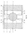
- Fig. 1a shows a plan view of a MEMS structure with a via torsion springs 56a-d and stiffening springs 53a-d to actuators 48a and 48b suspended micromirror 49.
- the dashed lines A-A ', BB' and CC ' indicate cross-sectional planes for which in Fig. 1b the structure of the MEMS structure is described in cross section.
- Fig. 1b shows for the cross-sectional plane AA 'the actuators 48a and 48b and the stiffening springs 53a and 53c, which have a greater thickness compared to the actuators 48a and 48b.
- the torsion springs 56a and 56c which have a smaller thickness than the stiffening springs 53a and 53c.
- the torsion springs 56a and 56c are more compliant to the movements induced by the actuators 48a and 48b than the stiffening springs 43a and 53c.
- the micromirror 49 arranged between the actuators 48a and 48b. This has an approximately equal thickness as the torsion springs 56a and 56c and the actuators 48a and 48b.
- Fig. 2 shows in the cross-sectional plane CC 'providing a stack 12 with a substrate 14, which is formed for example of a silicon layer.
- a first etching stop layer 22 is arranged, on whose surface facing away from the substrate 14 a first semiconductor layer 24 is arranged.
- the main side of the first semiconductor layer 24 facing away from the first etch stop layer 22 is covered by a second etch stop layer 26, to whose second main side remote from the first semiconductor layer 24 the second semiconductor layer 28 is again arranged.
- the prepared stack 12 is covered on an opposite side of the substrate 14, which defines an upper side of the stack 12, of an insulating layer, for example, a non-conductive etching layer, 32.
- the first and second semiconductor layers 24 and 28 of the stack 12 provided may be formed of polysilicon, whereas the first and second etch stop layers 22 and 26 may be silicon oxide.
- the insulating layer is formed of electrically non-conductive materials that prevent electrical contact of first electrodes 36 a and 36 b to the second semiconductor layer 28.
- the thicknesses of the first semiconductor layer 24 and the second semiconductor layer 28 are different and selected as required by the thickness of individual components of the later MEMS structure.
- a thickness of an etching stop layer is removed much slower than a semiconductor layer of comparable thickness. This makes it possible to remove uncovered areas of the respective semiconductor layer by masking lateral locations of a semiconductor layer from the mask, whereas areas covered by the mask are not removed because the etching process removes the comparatively thin etch stop mask only very slowly .
- By masking with a minimum and varying over the lateral extent thickness of the mask functional layers can be separated from each other.
- the minimum thickness of the etch stop layer is removed, residual axial dimensions remain in the sense of an etch stop mask, preventing masked area removal.
- the masking of the oxide layers can in particular be carried out so that island-like ⁇ tzstopp Schemee are formed.
- the first etching stop layer 22 has, in a lateral course, a region 34 along the lateral extent of which the first etching stop layer 22 has a greater thickness than in the remaining lateral course of the stack 12.
- the change in the layer thickness of the first etch stop layer 22 in the region 34 is formed stepwise.
- the first semiconductor layer 24 arranged on the first etching stop layer likewise has a variable layer thickness over a lateral extent of the layer 24, wherein the first semiconductor layer 24 in the region 34 is stepwise thinner to the extent thinner, in which the first ⁇ tzstopp GmbH 22 is formed thicker in the region 34, so that one of the first ⁇ tzstopptik 22 facing away from the main side of the first semiconductor layer is flat.
- the further layers 26, 28 and 32 also have planar surfaces.
- the stack 12 serves as the starting workpiece for the following process steps.
- the consecutive superposition of the individual layers is in the following Fig. 3 shown.
- Fig. 3a shows in the cross-sectional plane CC 'the arrangement of the substrate 14 and the arrangement of the first ⁇ tzstopp harsh 22 at a top defining the main side of the substrate 14.
- the substrate 14 forms with the top side of the substrate opposite the back side of the consecutively formed stack 12th
- back surfaces main sides of a layer or the stack 12 disposed facing away from the back side of the stack 12
- tops main sides of a layer facing the back side of the stack 12, respectively.
- the first etching stop layer 22 is arranged on the substrate in such a way that a step-like increase in the layer thickness is formed in the region 34 and a masking or mask is thus arranged. This forms a mask for the subsequent etching processes.
- a thermal oxidation process can be used for arranging the first etching stop layer 22 for example.
- Fig. 3b shows in the cross-sectional plane CC 'the subsequent step of the arrangement of the first semiconductor layer at the top of the first etching stop layer 22.
- the arranging can be carried out, for example, with an epitaxy method.
- the stepwise uneven implementation of the first etch stop layer 22 is compensated for by arranging the first semiconductor layer such that the top side of the first semiconductor layer 24 is planar. In the area 34 of the first semiconductor layer 24, this procedure results in the first semiconductor layer 24 being formed in the area 34 with a smaller thickness than in the course of its remaining lateral extent.
- the arrangement of the masking by the first etching stop layer 22 is not relevant insofar as the further layers can be deposited on a flat surface.
- Fig. 3c shows in the cross-sectional plane CC 'the arrangement of the second etching stop layer 26 on an upper side of the first semiconductor layer 24.
- Fig. 3d shows in the cross-sectional plane CC ', the arrangement of the second semiconductor layer 28 at an upper side of the second ⁇ tzstopp harsh 26.
- the second semiconductor layer 28 is arranged with a different layer of the first semiconductor layer 24, wherein in principle it is also conceivable that the first semiconductor layer 24 and the second semiconductor layer 28 have identical layer thicknesses.
- the substrate 14, the first etch stop layer 22, the first semiconductor layer 24, the second etch stop layer 26 and the second semiconductor layer 28 form the stack 12 after placement of the layers, which is provided for subsequent steps.
- Fig. 3e shows in the cross-sectional plane CC 'the arrangement of the insulating layer 32, over the lateral extent of the stack 12 to allow a konsekutive arrangement of functional layers.
- Fig. 4 shows in the cross-sectional plane CC ', the process step of the arrangement of first electrodes 36a and 36b, piezoelectric material 38a and 38b and second electrodes 42a and 42b on the stack 12 and a top of the insulating layer 32.
- first electrodes 36a and 36b At the top of the insulating layer 32 successively first electrodes 36a and 36b, piezoelectric material 38a and 38b and second electrodes 42a and 42b.
- the arrangement of the electrodes 36a, 36b, 42a and 42b is such that the piezoelectric material 38a is interposed between the first electrode 36a and the second electrode 42a and the piezoelectric material 38b is disposed between the first electrode 36b and the second electrode 42b.
- the second electrode 42a or 42b is arranged with respect to the first electrode 36a and 36b such that the second electrode 42a and 42b, respectively, the first electrode 36a and 36b is not touched and a short circuit is prevented.
- the insulation layer 32 is divided by a structuring 43 into a plurality of lateral regions 44a, 44b, 46a and 46b.
- the structuring 43 can be carried out, for example, by severing or cutting through the insulation layer 32.
- the areas 44a and 44b are thereby areas to be exposed, while the areas 46a and 46b are formed into actuator areas.
- the insulation layer 32 is removed, for example by a grinding or etching process.
- a reflection layer 47 is arranged on the upper side of the second semiconductor layer 28. This may for example comprise an aluminum or silver layer to reflect an incident light power, possibly a laser beam. If the structure formed from the stack 12 is used for a non-optical application, it may be possible to dispense with a reflective surface.
- Fig. 5 In the cross-sectional plane CC ', the removal of the second semiconductor layer 28, the second etch stop layer 26 and the first semiconductor layer 24 in the regions to be exposed 44a and 44b from the top of the second semiconductor layer 28.
- the removal can be carried out, for example, by an etching process.
- the first semiconductor layer 24, the second etch stop layer 26, the second semiconductor layer 28 and the insulating layer 32 are cut through in the lateral direction along the course of the structuring 43, wherein in the region 34 on the second semiconductor layer Reflection layer 47 is arranged.
- FIG. 12 shows the step of removing the substrate 14, the first semiconductor layer 24, and parts of the first etch stop layer 22 from the back side of the stack in the cross-sectional plane CC '.
- An etching process can also be used for the removal, which first flatly removes the substrate 14 in the regions 46a, 46b, 44a, 44b and 34. Subsequently, the first etching stop layer 22 is removed or etched away in precisely those regions. If the first etch stop layer 22 is removed in the regions 46a, 44a, 44b and 46b, the regions 44a and 44b are completely exposed in the axial direction.
- the absence of the etch stop layer 22 causes the removal, eg, the etch process, to consecutively attack the first semiconductor layer 24.
- the first semiconductor layer 24 is further covered with the first etch stop layer 22 from the rear side of the stack.
- the first electrodes 36a and 36b By partially removing the layers in the actuator regions 46a and 46b, the second etch stop layer 26, the second semiconductor layer 28, and the insulating layer 32, the first electrodes 36a and 36b, remain the piezoelectric ones Materials 38a and 38b and the second electrodes 42a and 42b in the axial courses of the actuator regions 46a and 46b.
- the actuators 48a and 48b are designed such that an application of an electrical voltage between the first electrode 36a or respectively 36b and the second electrode 42a or 42b leads to a deformation of the piezoelectric material 38a or 38b. This deformation, for example a contraction, of the piezoelectric material 36a or 36b leads to a deflection of the layers arranged on the first electrode, which then behave like a bending beam.
- the actuators 48a and 48b are supported on the peripheral region 52a and 52b.
- the areas 52a and 52b may be part of the initial stack or subsequently arranged. They are designed to form an anchor point of the spring-mass system formed by the preceding method steps.
- the layers remaining in the axial course of the region 34 form the micromirror 49 with the reflection layer 47.
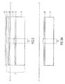
- Fig. 7 shows an alternative, produced by the described method, MEMS structure 10 in the cross-sectional plane A-A '.
- the substrate 14, the first etch stop layer 22, the first semiconductor layer 24, and the second etch stop layer 26 are removed by backside removal.
- the second etch stop layer 26 is further arranged so that stiffening springs 53a and 53b of the MEMS structure are larger in thickness than the actuators 48a and 48b, neglecting the electrodes and piezoelectric functional layers.
- the second etch stop layer 26 is removed by the locally selective process in the actuator regions 46a and 46b and in the region between the stiffening spring regions 54a and 54b.
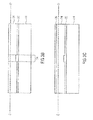
- Fig. 8 shows a cross-sectional view of the MEMS structure 10 in the cross-sectional plane B-B ', in which torsion springs 56a and 56b in the torsion spring portions 58a and 58b are shown.
- torsion spring regions 58a and 58b with the exception of the second semiconductor layer 26, all the other layers of the stack are removed, wherein, for example, by selective etching from the rear side of the stack 12, the torsion springs 56a and 56b are formed.
- torsion springs 56a and 56b are formed only by the second semiconductor layer 28, it is also conceivable that during the removal of layers from the backside of the stack, the second etch stop layer 26, the first semiconductor layer 24, or the first etch stop layer 22 respectively overlap those in the stack disposed Layers remains. In principle, different sequences of layers can be removed at different locations via the lateral extent and in different cross-sectional planes of the layers.
- the stack of material layers in previous embodiments always comprises the first and the second semiconductor layer, it is possible for the stack to be formed from a plurality of semiconductor layers with and / or without etch stop layers disposed therebetween.
- the manufacturing method of the preceding embodiments allows the fabrication of a MEMS structure having a mutually different layer thickness in the regions of the torsion spring 58a and 58b and the regions of the stiffening spring 54a and 54b.
- MEMS structure with a vibrationally suspended micromirror
- other MEMS structures for example mechanical microdrives, can be produced using the method described.
- the geometry of MEMS structures is very important to their overall performance. This makes it useful to construct different parts of a structure with different layer thicknesses depending on the assigned function.
- the process method described by the exemplary embodiments allows a precise definition and at the same time a broad feasible layer thickness range of the different layer thicknesses in a MEMS structure.
- a time-controlled etching process is not sufficient.
- double polysilicon layers arranged on a substrate are used instead of normal SOI wafers.
- an oxide layer is arranged in each case, which acts as an etch stop for the backside etching.
- the wafer is locally etched during the backside etch.
- the layer thicknesses of the MEMS structure are defined by the thicknesses of the polysilicon layers and the thicknesses of the etching stop layers, so that both layer thicknesses in different lateral areas and the contour of these areas can be precisely adjusted.
- the ability to fabricate a MEMS structure with multiple, different layer thicknesses significantly increases the degrees of freedom in the design of the structures.
- the oxide layers can be masked between individual polysilicon and / or silicon layers and thus have a variable layer thickness
- the surface of the stack of layers nevertheless has a flat surface, piezoelectric functional layers can be deposited on the topmost layer of the stack, which improves the quality significantly increased manufacturing processes.
Landscapes
- Engineering & Computer Science (AREA)
- Microelectronics & Electronic Packaging (AREA)
- Physics & Mathematics (AREA)
- Geometry (AREA)
- Manufacturing & Machinery (AREA)
- Chemical & Material Sciences (AREA)
- Analytical Chemistry (AREA)
- Computer Hardware Design (AREA)
- Micromachines (AREA)
Priority Applications (1)
| Application Number | Priority Date | Filing Date | Title |
|---|---|---|---|
| EP17205899.2A EP3312136B1 (fr) | 2013-05-17 | 2014-05-16 | Dispositif doté d'un ressort et d'un élément suspendu audit ressort et son procédé de fabrication |
Applications Claiming Priority (1)
| Application Number | Priority Date | Filing Date | Title |
|---|---|---|---|
| DE102013209238.5A DE102013209238B4 (de) | 2013-05-17 | 2013-05-17 | MEMS-Struktur und Verfahren zum Herstellen derselben |
Related Child Applications (2)
| Application Number | Title | Priority Date | Filing Date |
|---|---|---|---|
| EP17205899.2A Division-Into EP3312136B1 (fr) | 2013-05-17 | 2014-05-16 | Dispositif doté d'un ressort et d'un élément suspendu audit ressort et son procédé de fabrication |
| EP17205899.2A Division EP3312136B1 (fr) | 2013-05-17 | 2014-05-16 | Dispositif doté d'un ressort et d'un élément suspendu audit ressort et son procédé de fabrication |
Publications (3)
| Publication Number | Publication Date |
|---|---|
| EP2803635A2 true EP2803635A2 (fr) | 2014-11-19 |
| EP2803635A3 EP2803635A3 (fr) | 2016-10-26 |
| EP2803635B1 EP2803635B1 (fr) | 2019-02-06 |
Family
ID=50721672
Family Applications (2)
| Application Number | Title | Priority Date | Filing Date |
|---|---|---|---|
| EP14168566.9A Active EP2803635B1 (fr) | 2013-05-17 | 2014-05-16 | Dispositif ayant un ressort supportant un élément, et méthode de fabrication de celui-ci |
| EP17205899.2A Active EP3312136B1 (fr) | 2013-05-17 | 2014-05-16 | Dispositif doté d'un ressort et d'un élément suspendu audit ressort et son procédé de fabrication |
Family Applications After (1)
| Application Number | Title | Priority Date | Filing Date |
|---|---|---|---|
| EP17205899.2A Active EP3312136B1 (fr) | 2013-05-17 | 2014-05-16 | Dispositif doté d'un ressort et d'un élément suspendu audit ressort et son procédé de fabrication |
Country Status (4)
| Country | Link |
|---|---|
| US (1) | US9399573B2 (fr) |
| EP (2) | EP2803635B1 (fr) |
| CN (1) | CN104167433B (fr) |
| DE (1) | DE102013209238B4 (fr) |
Families Citing this family (3)
| Publication number | Priority date | Publication date | Assignee | Title |
|---|---|---|---|---|
| JP6390522B2 (ja) * | 2015-06-03 | 2018-09-19 | 株式会社デンソー | 光走査装置 |
| CN108604008B (zh) * | 2016-02-17 | 2020-11-10 | 三菱电机株式会社 | 反射镜驱动装置、反射镜驱动装置的控制方法及反射镜驱动装置的制造方法 |
| CN110577185B (zh) * | 2019-08-06 | 2021-11-16 | 西人马联合测控(泉州)科技有限公司 | Mems结构、mems结构的制作方法及胎压传感器 |
Family Cites Families (17)
| Publication number | Priority date | Publication date | Assignee | Title |
|---|---|---|---|---|
| US6535318B1 (en) * | 1999-11-12 | 2003-03-18 | Jds Uniphase Corporation | Integrated optoelectronic devices having pop-up mirrors therein and methods of forming and operating same |
| US6628041B2 (en) * | 2000-05-16 | 2003-09-30 | Calient Networks, Inc. | Micro-electro-mechanical-system (MEMS) mirror device having large angle out of plane motion using shaped combed finger actuators and method for fabricating the same |
| US20020054729A1 (en) * | 2000-11-03 | 2002-05-09 | Berg John S. | Piezoelectric optical switch |
| JP3827977B2 (ja) * | 2001-08-20 | 2006-09-27 | 富士通株式会社 | マイクロミラー素子の製造方法 |
| US8691099B2 (en) * | 2001-12-13 | 2014-04-08 | John Gritters | Process for fabricating MEMS devices |
| JP3987382B2 (ja) * | 2002-06-11 | 2007-10-10 | 富士通株式会社 | マイクロミラー素子およびその製造方法 |
| JP4102158B2 (ja) * | 2002-10-24 | 2008-06-18 | 富士通株式会社 | マイクロ構造体の製造方法 |
| EP1424583A3 (fr) * | 2002-11-26 | 2004-06-09 | LG Electronics Inc. | Récepteur optique et émetteur optique utilisant un attenuateur de lumière variable, procédé de production d'un attenuateur de lumière variable |
| JP4573664B2 (ja) * | 2005-02-16 | 2010-11-04 | 富士通株式会社 | マイクロ揺動素子およびその製造方法 |
| US20080169522A1 (en) * | 2007-01-17 | 2008-07-17 | Olympus Corporation | Moving element and method of manufacturing the same |
| WO2008090921A1 (fr) * | 2007-01-26 | 2008-07-31 | Panasonic Electric Works Co., Ltd. | Miroir de balayage optique, structure semi-conductrice et procédé pour fabriquer ceux-ci |
| EP2100848A1 (fr) * | 2008-03-11 | 2009-09-16 | Fraunhofer-Gesellschaft zur Förderung der Angewandten Forschung e.V. | Composant micromécanique ayant un mirroir et son procédé de fabrication |
| DE102008026886B4 (de) * | 2008-06-05 | 2016-04-28 | Fraunhofer-Gesellschaft zur Förderung der angewandten Forschung e.V. | Verfahren zur Strukturierung einer Nutzschicht eines Substrats |
| DE09770219T8 (de) * | 2008-06-25 | 2013-04-25 | Panasonic Electric Works Co., Ltd. | Bewegliche struktur und lichtabtastspiegel damit |
| DE102008041178B4 (de) | 2008-08-12 | 2018-11-15 | Robert Bosch Gmbh | Herstellungsverfahren für ein mikromechanisches Bauteil |
| US8555719B2 (en) * | 2011-01-24 | 2013-10-15 | Freescale Semiconductor, Inc. | MEMS sensor with folded torsion springs |
| DE102011081002B4 (de) * | 2011-08-16 | 2020-01-16 | Robert Bosch Gmbh | Herstellungsverfahren für ein mikromechanisches Bauteil |
-
2013
- 2013-05-17 DE DE102013209238.5A patent/DE102013209238B4/de not_active Expired - Fee Related
-
2014
- 2014-05-16 EP EP14168566.9A patent/EP2803635B1/fr active Active
- 2014-05-16 EP EP17205899.2A patent/EP3312136B1/fr active Active
- 2014-05-16 US US14/280,154 patent/US9399573B2/en active Active
- 2014-05-19 CN CN201410260339.5A patent/CN104167433B/zh active Active
Non-Patent Citations (1)
| Title |
|---|
| None |
Also Published As
| Publication number | Publication date |
|---|---|
| DE102013209238A1 (de) | 2014-11-20 |
| CN104167433B (zh) | 2017-04-26 |
| EP2803635B1 (fr) | 2019-02-06 |
| US9399573B2 (en) | 2016-07-26 |
| CN104167433A (zh) | 2014-11-26 |
| EP2803635A3 (fr) | 2016-10-26 |
| US20140339658A1 (en) | 2014-11-20 |
| EP3312136A1 (fr) | 2018-04-25 |
| EP3312136B1 (fr) | 2020-05-13 |
| DE102013209238B4 (de) | 2017-10-12 |
Similar Documents
| Publication | Publication Date | Title |
|---|---|---|
| DE19921241B4 (de) | Verfahren zur Herstellung eines Halbleitersensors für eine dynamische Größe | |
| DE60200251T2 (de) | Optischer Scanner und Herstellungsverfahren dafür | |
| EP1550349B1 (fr) | Membrane et procede de realisation associe | |
| EP3186887B1 (fr) | Filtre sur puce et procédé de fabrication d'un filtre sur puce | |
| DE10207328A1 (de) | Verfahren zum Liefern unterschiedlicher Frequenzeinstellungen bei einem akustischen Dünnfilmvolumenresonator- (FBAR-) Filter und Vorrichtung, die das Verfahren beinhaltet | |
| DE10207342A1 (de) | Verfahren zum Liefern unterschiedlicher Frequenzeinstellungen bei einem akustischen Dünnfilmvolumenresonator- (FBAR-) Filter und Vorrichtung, die das Verfahren beinhaltet | |
| DE10160830A1 (de) | Mikromechanische Sensoren und Verfahren zur Herstellung derselben | |
| DE102010000818A1 (de) | MEMS-Resonatorbauelemente | |
| EP2026116A1 (fr) | Dispositif de micro-miroir | |
| DE102017215236A1 (de) | MEMS-Schalter und Verfahren zur Herstellung eines MEMS-Schalters | |
| EP2803635B1 (fr) | Dispositif ayant un ressort supportant un élément, et méthode de fabrication de celui-ci | |
| DE102015200629A1 (de) | Verfahren zur gleichzeigen Strukturierung und Chip-Vereinzelung | |
| DE60000565T2 (de) | Mikro-Elektromekanische Optische Vorrichtung | |
| DE10235371A1 (de) | Verfahren zur Herstellung einer mikromechanischen Vorrichtung, insbesondere einer mikromechanischen Schwingspiegelvorrichtung | |
| DE102020114347B3 (de) | MEMS-Vorrichtungen mit Federelement und Kammantrieb sowie zugehörige Herstellungsverfahren | |
| EP3931623B1 (fr) | Structure micromécanique et procédé de fourniture de celle-ci | |
| DE102015213714A1 (de) | Mikromechanisches Bauteil und Verfahren zur Herstellung eines piezoelektrischen mikromechanischen Bauteils | |
| DE112019007049B4 (de) | Optische abtastvorrichtung und verfahren zur herstellung derselben | |
| EP1402583B1 (fr) | Transducteur piezoelectrique de flexion | |
| DE112016006445B4 (de) | Spiegelantriebsvorrichtung sowie Verfahren zur Steuerung und Herstellung einer Spiegelantriebsvorrichtung | |
| DE102008001663B4 (de) | Mikromechanisches Bauteil und Herstellungsverfahren für ein mikromechanisches Bauteil | |
| DE102013212095A1 (de) | Mikro-elektromechanischer Reflektor und Verfahren zum Herstellen eines mikro-elektromechanischen Reflektors | |
| EP3887783B1 (fr) | Dispositif d'interférométrie et procédé de fabrication d'un dispositif d'interférométrie | |
| DE102023117699B4 (de) | Mikrostruktur aus Glas, Mikro-Mechanik und zugehörige Verwendung | |
| DE102019202658B3 (de) | Mikromechanische Struktur und Verfahren zum Bereitstellen derselben |
Legal Events
| Date | Code | Title | Description |
|---|---|---|---|
| PUAI | Public reference made under article 153(3) epc to a published international application that has entered the european phase |
Free format text: ORIGINAL CODE: 0009012 |
|
| 17P | Request for examination filed |
Effective date: 20140516 |
|
| AK | Designated contracting states |
Kind code of ref document: A2 Designated state(s): AL AT BE BG CH CY CZ DE DK EE ES FI FR GB GR HR HU IE IS IT LI LT LU LV MC MK MT NL NO PL PT RO RS SE SI SK SM TR |
|
| AX | Request for extension of the european patent |
Extension state: BA ME |
|
| PUAL | Search report despatched |
Free format text: ORIGINAL CODE: 0009013 |
|
| AK | Designated contracting states |
Kind code of ref document: A3 Designated state(s): AL AT BE BG CH CY CZ DE DK EE ES FI FR GB GR HR HU IE IS IT LI LT LU LV MC MK MT NL NO PL PT RO RS SE SI SK SM TR |
|
| AX | Request for extension of the european patent |
Extension state: BA ME |
|
| RIC1 | Information provided on ipc code assigned before grant |
Ipc: B81C 1/00 20060101AFI20160919BHEP |
|
| STAA | Information on the status of an ep patent application or granted ep patent |
Free format text: STATUS: REQUEST FOR EXAMINATION WAS MADE |
|
| R17P | Request for examination filed (corrected) |
Effective date: 20170424 |
|
| RBV | Designated contracting states (corrected) |
Designated state(s): AL AT BE BG CH CY CZ DE DK EE ES FI FR GB GR HR HU IE IS IT LI LT LU LV MC MK MT NL NO PL PT RO RS SE SI SK SM TR |
|
| STAA | Information on the status of an ep patent application or granted ep patent |
Free format text: STATUS: EXAMINATION IS IN PROGRESS |
|
| 17Q | First examination report despatched |
Effective date: 20170606 |
|
| GRAP | Despatch of communication of intention to grant a patent |
Free format text: ORIGINAL CODE: EPIDOSNIGR1 |
|
| STAA | Information on the status of an ep patent application or granted ep patent |
Free format text: STATUS: GRANT OF PATENT IS INTENDED |
|
| INTG | Intention to grant announced |
Effective date: 20180810 |
|
| GRAS | Grant fee paid |
Free format text: ORIGINAL CODE: EPIDOSNIGR3 |
|
| GRAA | (expected) grant |
Free format text: ORIGINAL CODE: 0009210 |
|
| STAA | Information on the status of an ep patent application or granted ep patent |
Free format text: STATUS: THE PATENT HAS BEEN GRANTED |
|
| AK | Designated contracting states |
Kind code of ref document: B1 Designated state(s): AL AT BE BG CH CY CZ DE DK EE ES FI FR GB GR HR HU IE IS IT LI LT LU LV MC MK MT NL NO PL PT RO RS SE SI SK SM TR |
|
| REG | Reference to a national code |
Ref country code: GB Ref legal event code: FG4D Free format text: NOT ENGLISH |
|
| REG | Reference to a national code |
Ref country code: CH Ref legal event code: EP Ref country code: AT Ref legal event code: REF Ref document number: 1094775 Country of ref document: AT Kind code of ref document: T Effective date: 20190215 |
|
| REG | Reference to a national code |
Ref country code: DE Ref legal event code: R096 Ref document number: 502014010741 Country of ref document: DE |
|
| REG | Reference to a national code |
Ref country code: IE Ref legal event code: FG4D Free format text: LANGUAGE OF EP DOCUMENT: GERMAN |
|
| REG | Reference to a national code |
Ref country code: NL Ref legal event code: MP Effective date: 20190206 |
|
| REG | Reference to a national code |
Ref country code: LT Ref legal event code: MG4D |
|
| PG25 | Lapsed in a contracting state [announced via postgrant information from national office to epo] |
Ref country code: PT Free format text: LAPSE BECAUSE OF FAILURE TO SUBMIT A TRANSLATION OF THE DESCRIPTION OR TO PAY THE FEE WITHIN THE PRESCRIBED TIME-LIMIT Effective date: 20190606 Ref country code: ES Free format text: LAPSE BECAUSE OF FAILURE TO SUBMIT A TRANSLATION OF THE DESCRIPTION OR TO PAY THE FEE WITHIN THE PRESCRIBED TIME-LIMIT Effective date: 20190206 Ref country code: LT Free format text: LAPSE BECAUSE OF FAILURE TO SUBMIT A TRANSLATION OF THE DESCRIPTION OR TO PAY THE FEE WITHIN THE PRESCRIBED TIME-LIMIT Effective date: 20190206 Ref country code: NL Free format text: LAPSE BECAUSE OF FAILURE TO SUBMIT A TRANSLATION OF THE DESCRIPTION OR TO PAY THE FEE WITHIN THE PRESCRIBED TIME-LIMIT Effective date: 20190206 Ref country code: NO Free format text: LAPSE BECAUSE OF FAILURE TO SUBMIT A TRANSLATION OF THE DESCRIPTION OR TO PAY THE FEE WITHIN THE PRESCRIBED TIME-LIMIT Effective date: 20190506 Ref country code: SE Free format text: LAPSE BECAUSE OF FAILURE TO SUBMIT A TRANSLATION OF THE DESCRIPTION OR TO PAY THE FEE WITHIN THE PRESCRIBED TIME-LIMIT Effective date: 20190206 Ref country code: FI Free format text: LAPSE BECAUSE OF FAILURE TO SUBMIT A TRANSLATION OF THE DESCRIPTION OR TO PAY THE FEE WITHIN THE PRESCRIBED TIME-LIMIT Effective date: 20190206 |
|
| PG25 | Lapsed in a contracting state [announced via postgrant information from national office to epo] |
Ref country code: GR Free format text: LAPSE BECAUSE OF FAILURE TO SUBMIT A TRANSLATION OF THE DESCRIPTION OR TO PAY THE FEE WITHIN THE PRESCRIBED TIME-LIMIT Effective date: 20190507 Ref country code: BG Free format text: LAPSE BECAUSE OF FAILURE TO SUBMIT A TRANSLATION OF THE DESCRIPTION OR TO PAY THE FEE WITHIN THE PRESCRIBED TIME-LIMIT Effective date: 20190506 Ref country code: HR Free format text: LAPSE BECAUSE OF FAILURE TO SUBMIT A TRANSLATION OF THE DESCRIPTION OR TO PAY THE FEE WITHIN THE PRESCRIBED TIME-LIMIT Effective date: 20190206 Ref country code: RS Free format text: LAPSE BECAUSE OF FAILURE TO SUBMIT A TRANSLATION OF THE DESCRIPTION OR TO PAY THE FEE WITHIN THE PRESCRIBED TIME-LIMIT Effective date: 20190206 Ref country code: IS Free format text: LAPSE BECAUSE OF FAILURE TO SUBMIT A TRANSLATION OF THE DESCRIPTION OR TO PAY THE FEE WITHIN THE PRESCRIBED TIME-LIMIT Effective date: 20190606 Ref country code: LV Free format text: LAPSE BECAUSE OF FAILURE TO SUBMIT A TRANSLATION OF THE DESCRIPTION OR TO PAY THE FEE WITHIN THE PRESCRIBED TIME-LIMIT Effective date: 20190206 |
|
| PG25 | Lapsed in a contracting state [announced via postgrant information from national office to epo] |
Ref country code: SK Free format text: LAPSE BECAUSE OF FAILURE TO SUBMIT A TRANSLATION OF THE DESCRIPTION OR TO PAY THE FEE WITHIN THE PRESCRIBED TIME-LIMIT Effective date: 20190206 Ref country code: RO Free format text: LAPSE BECAUSE OF FAILURE TO SUBMIT A TRANSLATION OF THE DESCRIPTION OR TO PAY THE FEE WITHIN THE PRESCRIBED TIME-LIMIT Effective date: 20190206 Ref country code: IT Free format text: LAPSE BECAUSE OF FAILURE TO SUBMIT A TRANSLATION OF THE DESCRIPTION OR TO PAY THE FEE WITHIN THE PRESCRIBED TIME-LIMIT Effective date: 20190206 Ref country code: CZ Free format text: LAPSE BECAUSE OF FAILURE TO SUBMIT A TRANSLATION OF THE DESCRIPTION OR TO PAY THE FEE WITHIN THE PRESCRIBED TIME-LIMIT Effective date: 20190206 Ref country code: DK Free format text: LAPSE BECAUSE OF FAILURE TO SUBMIT A TRANSLATION OF THE DESCRIPTION OR TO PAY THE FEE WITHIN THE PRESCRIBED TIME-LIMIT Effective date: 20190206 Ref country code: AL Free format text: LAPSE BECAUSE OF FAILURE TO SUBMIT A TRANSLATION OF THE DESCRIPTION OR TO PAY THE FEE WITHIN THE PRESCRIBED TIME-LIMIT Effective date: 20190206 Ref country code: EE Free format text: LAPSE BECAUSE OF FAILURE TO SUBMIT A TRANSLATION OF THE DESCRIPTION OR TO PAY THE FEE WITHIN THE PRESCRIBED TIME-LIMIT Effective date: 20190206 |
|
| REG | Reference to a national code |
Ref country code: DE Ref legal event code: R097 Ref document number: 502014010741 Country of ref document: DE |
|
| PG25 | Lapsed in a contracting state [announced via postgrant information from national office to epo] |
Ref country code: SM Free format text: LAPSE BECAUSE OF FAILURE TO SUBMIT A TRANSLATION OF THE DESCRIPTION OR TO PAY THE FEE WITHIN THE PRESCRIBED TIME-LIMIT Effective date: 20190206 Ref country code: PL Free format text: LAPSE BECAUSE OF FAILURE TO SUBMIT A TRANSLATION OF THE DESCRIPTION OR TO PAY THE FEE WITHIN THE PRESCRIBED TIME-LIMIT Effective date: 20190206 |
|
| PLBE | No opposition filed within time limit |
Free format text: ORIGINAL CODE: 0009261 |
|
| STAA | Information on the status of an ep patent application or granted ep patent |
Free format text: STATUS: NO OPPOSITION FILED WITHIN TIME LIMIT |
|
| REG | Reference to a national code |
Ref country code: CH Ref legal event code: PL |
|
| 26N | No opposition filed |
Effective date: 20191107 |
|
| PG25 | Lapsed in a contracting state [announced via postgrant information from national office to epo] |
Ref country code: CH Free format text: LAPSE BECAUSE OF NON-PAYMENT OF DUE FEES Effective date: 20190531 Ref country code: MC Free format text: LAPSE BECAUSE OF FAILURE TO SUBMIT A TRANSLATION OF THE DESCRIPTION OR TO PAY THE FEE WITHIN THE PRESCRIBED TIME-LIMIT Effective date: 20190206 Ref country code: LI Free format text: LAPSE BECAUSE OF NON-PAYMENT OF DUE FEES Effective date: 20190531 |
|
| REG | Reference to a national code |
Ref country code: BE Ref legal event code: MM Effective date: 20190531 |
|
| PG25 | Lapsed in a contracting state [announced via postgrant information from national office to epo] |
Ref country code: SI Free format text: LAPSE BECAUSE OF FAILURE TO SUBMIT A TRANSLATION OF THE DESCRIPTION OR TO PAY THE FEE WITHIN THE PRESCRIBED TIME-LIMIT Effective date: 20190206 Ref country code: LU Free format text: LAPSE BECAUSE OF NON-PAYMENT OF DUE FEES Effective date: 20190516 |
|
| PG25 | Lapsed in a contracting state [announced via postgrant information from national office to epo] |
Ref country code: TR Free format text: LAPSE BECAUSE OF FAILURE TO SUBMIT A TRANSLATION OF THE DESCRIPTION OR TO PAY THE FEE WITHIN THE PRESCRIBED TIME-LIMIT Effective date: 20190206 |
|
| PG25 | Lapsed in a contracting state [announced via postgrant information from national office to epo] |
Ref country code: IE Free format text: LAPSE BECAUSE OF NON-PAYMENT OF DUE FEES Effective date: 20190516 |
|
| PG25 | Lapsed in a contracting state [announced via postgrant information from national office to epo] |
Ref country code: BE Free format text: LAPSE BECAUSE OF NON-PAYMENT OF DUE FEES Effective date: 20190531 |
|
| REG | Reference to a national code |
Ref country code: AT Ref legal event code: MM01 Ref document number: 1094775 Country of ref document: AT Kind code of ref document: T Effective date: 20190516 |
|
| PG25 | Lapsed in a contracting state [announced via postgrant information from national office to epo] |
Ref country code: AT Free format text: LAPSE BECAUSE OF NON-PAYMENT OF DUE FEES Effective date: 20190516 |
|
| PG25 | Lapsed in a contracting state [announced via postgrant information from national office to epo] |
Ref country code: CY Free format text: LAPSE BECAUSE OF FAILURE TO SUBMIT A TRANSLATION OF THE DESCRIPTION OR TO PAY THE FEE WITHIN THE PRESCRIBED TIME-LIMIT Effective date: 20190206 |
|
| PG25 | Lapsed in a contracting state [announced via postgrant information from national office to epo] |
Ref country code: HU Free format text: LAPSE BECAUSE OF FAILURE TO SUBMIT A TRANSLATION OF THE DESCRIPTION OR TO PAY THE FEE WITHIN THE PRESCRIBED TIME-LIMIT; INVALID AB INITIO Effective date: 20140516 Ref country code: MT Free format text: LAPSE BECAUSE OF FAILURE TO SUBMIT A TRANSLATION OF THE DESCRIPTION OR TO PAY THE FEE WITHIN THE PRESCRIBED TIME-LIMIT Effective date: 20190206 |
|
| PG25 | Lapsed in a contracting state [announced via postgrant information from national office to epo] |
Ref country code: MK Free format text: LAPSE BECAUSE OF FAILURE TO SUBMIT A TRANSLATION OF THE DESCRIPTION OR TO PAY THE FEE WITHIN THE PRESCRIBED TIME-LIMIT Effective date: 20190206 |
|
| P01 | Opt-out of the competence of the unified patent court (upc) registered |
Effective date: 20230524 |
|
| PGFP | Annual fee paid to national office [announced via postgrant information from national office to epo] |
Ref country code: DE Payment date: 20250519 Year of fee payment: 12 |
|
| PGFP | Annual fee paid to national office [announced via postgrant information from national office to epo] |
Ref country code: GB Payment date: 20250522 Year of fee payment: 12 |
|
| PGFP | Annual fee paid to national office [announced via postgrant information from national office to epo] |
Ref country code: FR Payment date: 20250526 Year of fee payment: 12 |