EP2803714A1 - SiAlON:Ce luminophore - Google Patents
SiAlON:Ce luminophore Download PDFInfo
- Publication number
- EP2803714A1 EP2803714A1 EP14155376.8A EP14155376A EP2803714A1 EP 2803714 A1 EP2803714 A1 EP 2803714A1 EP 14155376 A EP14155376 A EP 14155376A EP 2803714 A1 EP2803714 A1 EP 2803714A1
- Authority
- EP
- European Patent Office
- Prior art keywords
- phosphor
- light
- emitting
- emitting device
- satisfies
- Prior art date
- Legal status (The legal status is an assumption and is not a legal conclusion. Google has not performed a legal analysis and makes no representation as to the accuracy of the status listed.)
- Withdrawn
Links
Images




Classifications
-
- H—ELECTRICITY
- H10—SEMICONDUCTOR DEVICES; ELECTRIC SOLID-STATE DEVICES NOT OTHERWISE PROVIDED FOR
- H10H—INORGANIC LIGHT-EMITTING SEMICONDUCTOR DEVICES HAVING POTENTIAL BARRIERS
- H10H20/00—Individual inorganic light-emitting semiconductor devices having potential barriers, e.g. light-emitting diodes [LED]
- H10H20/80—Constructional details
- H10H20/85—Packages
- H10H20/851—Wavelength conversion means
- H10H20/8511—Wavelength conversion means characterised by their material, e.g. binder
- H10H20/8512—Wavelength conversion materials
-
- C—CHEMISTRY; METALLURGY
- C04—CEMENTS; CONCRETE; ARTIFICIAL STONE; CERAMICS; REFRACTORIES
- C04B—LIME, MAGNESIA; SLAG; CEMENTS; COMPOSITIONS THEREOF, e.g. MORTARS, CONCRETE OR LIKE BUILDING MATERIALS; ARTIFICIAL STONE; CERAMICS; REFRACTORIES; TREATMENT OF NATURAL STONE
- C04B35/00—Shaped ceramic products characterised by their composition; Ceramics compositions; Processing powders of inorganic compounds preparatory to the manufacturing of ceramic products
- C04B35/515—Shaped ceramic products characterised by their composition; Ceramics compositions; Processing powders of inorganic compounds preparatory to the manufacturing of ceramic products based on non-oxide ceramics
- C04B35/58—Shaped ceramic products characterised by their composition; Ceramics compositions; Processing powders of inorganic compounds preparatory to the manufacturing of ceramic products based on non-oxide ceramics based on borides, nitrides, i.e. nitrides, oxynitrides, carbonitrides or oxycarbonitrides or silicides
- C04B35/597—Shaped ceramic products characterised by their composition; Ceramics compositions; Processing powders of inorganic compounds preparatory to the manufacturing of ceramic products based on non-oxide ceramics based on borides, nitrides, i.e. nitrides, oxynitrides, carbonitrides or oxycarbonitrides or silicides based on silicon oxynitride, e.g. SIALONS
-
- C—CHEMISTRY; METALLURGY
- C04—CEMENTS; CONCRETE; ARTIFICIAL STONE; CERAMICS; REFRACTORIES
- C04B—LIME, MAGNESIA; SLAG; CEMENTS; COMPOSITIONS THEREOF, e.g. MORTARS, CONCRETE OR LIKE BUILDING MATERIALS; ARTIFICIAL STONE; CERAMICS; REFRACTORIES; TREATMENT OF NATURAL STONE
- C04B35/00—Shaped ceramic products characterised by their composition; Ceramics compositions; Processing powders of inorganic compounds preparatory to the manufacturing of ceramic products
- C04B35/622—Forming processes; Processing powders of inorganic compounds preparatory to the manufacturing of ceramic products
- C04B35/626—Preparing or treating the powders individually or as batches ; preparing or treating macroscopic reinforcing agents for ceramic products, e.g. fibres; mechanical aspects section B
- C04B35/62605—Treating the starting powders individually or as mixtures
- C04B35/62645—Thermal treatment of powders or mixtures thereof other than sintering
- C04B35/6268—Thermal treatment of powders or mixtures thereof other than sintering characterised by the applied pressure or type of atmosphere, e.g. in vacuum, hydrogen or a specific oxygen pressure
-
- C—CHEMISTRY; METALLURGY
- C09—DYES; PAINTS; POLISHES; NATURAL RESINS; ADHESIVES; COMPOSITIONS NOT OTHERWISE PROVIDED FOR; APPLICATIONS OF MATERIALS NOT OTHERWISE PROVIDED FOR
- C09K—MATERIALS FOR MISCELLANEOUS APPLICATIONS, NOT PROVIDED FOR ELSEWHERE
- C09K11/00—Luminescent materials, e.g. electroluminescent or chemiluminescent
- C09K11/08—Luminescent materials, e.g. electroluminescent or chemiluminescent containing inorganic luminescent materials
- C09K11/0883—Arsenides; Nitrides; Phosphides
-
- C—CHEMISTRY; METALLURGY
- C09—DYES; PAINTS; POLISHES; NATURAL RESINS; ADHESIVES; COMPOSITIONS NOT OTHERWISE PROVIDED FOR; APPLICATIONS OF MATERIALS NOT OTHERWISE PROVIDED FOR
- C09K—MATERIALS FOR MISCELLANEOUS APPLICATIONS, NOT PROVIDED FOR ELSEWHERE
- C09K11/00—Luminescent materials, e.g. electroluminescent or chemiluminescent
- C09K11/08—Luminescent materials, e.g. electroluminescent or chemiluminescent containing inorganic luminescent materials
- C09K11/77—Luminescent materials, e.g. electroluminescent or chemiluminescent containing inorganic luminescent materials containing rare earth metals
- C09K11/7715—Luminescent materials, e.g. electroluminescent or chemiluminescent containing inorganic luminescent materials containing rare earth metals containing cerium
- C09K11/77218—Silicon Aluminium Nitrides or Silicon Aluminium Oxynitrides
-
- H—ELECTRICITY
- H10—SEMICONDUCTOR DEVICES; ELECTRIC SOLID-STATE DEVICES NOT OTHERWISE PROVIDED FOR
- H10H—INORGANIC LIGHT-EMITTING SEMICONDUCTOR DEVICES HAVING POTENTIAL BARRIERS
- H10H20/00—Individual inorganic light-emitting semiconductor devices having potential barriers, e.g. light-emitting diodes [LED]
- H10H20/01—Manufacture or treatment
-
- H—ELECTRICITY
- H10—SEMICONDUCTOR DEVICES; ELECTRIC SOLID-STATE DEVICES NOT OTHERWISE PROVIDED FOR
- H10H—INORGANIC LIGHT-EMITTING SEMICONDUCTOR DEVICES HAVING POTENTIAL BARRIERS
- H10H20/00—Individual inorganic light-emitting semiconductor devices having potential barriers, e.g. light-emitting diodes [LED]
- H10H20/80—Constructional details
- H10H20/84—Coatings, e.g. passivation layers or antireflective coatings
-
- C—CHEMISTRY; METALLURGY
- C04—CEMENTS; CONCRETE; ARTIFICIAL STONE; CERAMICS; REFRACTORIES
- C04B—LIME, MAGNESIA; SLAG; CEMENTS; COMPOSITIONS THEREOF, e.g. MORTARS, CONCRETE OR LIKE BUILDING MATERIALS; ARTIFICIAL STONE; CERAMICS; REFRACTORIES; TREATMENT OF NATURAL STONE
- C04B2235/00—Aspects relating to ceramic starting mixtures or sintered ceramic products
- C04B2235/02—Composition of constituents of the starting material or of secondary phases of the final product
- C04B2235/30—Constituents and secondary phases not being of a fibrous nature
- C04B2235/32—Metal oxides, mixed metal oxides, or oxide-forming salts thereof, e.g. carbonates, nitrates, (oxy)hydroxides, chlorides
- C04B2235/3217—Aluminum oxide or oxide forming salts thereof, e.g. bauxite, alpha-alumina
-
- C—CHEMISTRY; METALLURGY
- C04—CEMENTS; CONCRETE; ARTIFICIAL STONE; CERAMICS; REFRACTORIES
- C04B—LIME, MAGNESIA; SLAG; CEMENTS; COMPOSITIONS THEREOF, e.g. MORTARS, CONCRETE OR LIKE BUILDING MATERIALS; ARTIFICIAL STONE; CERAMICS; REFRACTORIES; TREATMENT OF NATURAL STONE
- C04B2235/00—Aspects relating to ceramic starting mixtures or sintered ceramic products
- C04B2235/02—Composition of constituents of the starting material or of secondary phases of the final product
- C04B2235/30—Constituents and secondary phases not being of a fibrous nature
- C04B2235/32—Metal oxides, mixed metal oxides, or oxide-forming salts thereof, e.g. carbonates, nitrates, (oxy)hydroxides, chlorides
- C04B2235/3224—Rare earth oxide or oxide forming salts thereof, e.g. scandium oxide
- C04B2235/3229—Cerium oxides or oxide-forming salts thereof
-
- C—CHEMISTRY; METALLURGY
- C04—CEMENTS; CONCRETE; ARTIFICIAL STONE; CERAMICS; REFRACTORIES
- C04B—LIME, MAGNESIA; SLAG; CEMENTS; COMPOSITIONS THEREOF, e.g. MORTARS, CONCRETE OR LIKE BUILDING MATERIALS; ARTIFICIAL STONE; CERAMICS; REFRACTORIES; TREATMENT OF NATURAL STONE
- C04B2235/00—Aspects relating to ceramic starting mixtures or sintered ceramic products
- C04B2235/02—Composition of constituents of the starting material or of secondary phases of the final product
- C04B2235/30—Constituents and secondary phases not being of a fibrous nature
- C04B2235/38—Non-oxide ceramic constituents or additives
- C04B2235/3852—Nitrides, e.g. oxynitrides, carbonitrides, oxycarbonitrides, lithium nitride, magnesium nitride
-
- C—CHEMISTRY; METALLURGY
- C04—CEMENTS; CONCRETE; ARTIFICIAL STONE; CERAMICS; REFRACTORIES
- C04B—LIME, MAGNESIA; SLAG; CEMENTS; COMPOSITIONS THEREOF, e.g. MORTARS, CONCRETE OR LIKE BUILDING MATERIALS; ARTIFICIAL STONE; CERAMICS; REFRACTORIES; TREATMENT OF NATURAL STONE
- C04B2235/00—Aspects relating to ceramic starting mixtures or sintered ceramic products
- C04B2235/02—Composition of constituents of the starting material or of secondary phases of the final product
- C04B2235/30—Constituents and secondary phases not being of a fibrous nature
- C04B2235/38—Non-oxide ceramic constituents or additives
- C04B2235/3852—Nitrides, e.g. oxynitrides, carbonitrides, oxycarbonitrides, lithium nitride, magnesium nitride
- C04B2235/3865—Aluminium nitrides
-
- C—CHEMISTRY; METALLURGY
- C04—CEMENTS; CONCRETE; ARTIFICIAL STONE; CERAMICS; REFRACTORIES
- C04B—LIME, MAGNESIA; SLAG; CEMENTS; COMPOSITIONS THEREOF, e.g. MORTARS, CONCRETE OR LIKE BUILDING MATERIALS; ARTIFICIAL STONE; CERAMICS; REFRACTORIES; TREATMENT OF NATURAL STONE
- C04B2235/00—Aspects relating to ceramic starting mixtures or sintered ceramic products
- C04B2235/02—Composition of constituents of the starting material or of secondary phases of the final product
- C04B2235/30—Constituents and secondary phases not being of a fibrous nature
- C04B2235/38—Non-oxide ceramic constituents or additives
- C04B2235/3852—Nitrides, e.g. oxynitrides, carbonitrides, oxycarbonitrides, lithium nitride, magnesium nitride
- C04B2235/3873—Silicon nitrides, e.g. silicon carbonitride, silicon oxynitride
-
- C—CHEMISTRY; METALLURGY
- C04—CEMENTS; CONCRETE; ARTIFICIAL STONE; CERAMICS; REFRACTORIES
- C04B—LIME, MAGNESIA; SLAG; CEMENTS; COMPOSITIONS THEREOF, e.g. MORTARS, CONCRETE OR LIKE BUILDING MATERIALS; ARTIFICIAL STONE; CERAMICS; REFRACTORIES; TREATMENT OF NATURAL STONE
- C04B2235/00—Aspects relating to ceramic starting mixtures or sintered ceramic products
- C04B2235/02—Composition of constituents of the starting material or of secondary phases of the final product
- C04B2235/30—Constituents and secondary phases not being of a fibrous nature
- C04B2235/44—Metal salt constituents or additives chosen for the nature of the anions, e.g. hydrides or acetylacetonate
- C04B2235/444—Halide containing anions, e.g. bromide, iodate, chlorite
-
- C—CHEMISTRY; METALLURGY
- C04—CEMENTS; CONCRETE; ARTIFICIAL STONE; CERAMICS; REFRACTORIES
- C04B—LIME, MAGNESIA; SLAG; CEMENTS; COMPOSITIONS THEREOF, e.g. MORTARS, CONCRETE OR LIKE BUILDING MATERIALS; ARTIFICIAL STONE; CERAMICS; REFRACTORIES; TREATMENT OF NATURAL STONE
- C04B2235/00—Aspects relating to ceramic starting mixtures or sintered ceramic products
- C04B2235/02—Composition of constituents of the starting material or of secondary phases of the final product
- C04B2235/50—Constituents or additives of the starting mixture chosen for their shape or used because of their shape or their physical appearance
- C04B2235/52—Constituents or additives characterised by their shapes
- C04B2235/5296—Constituents or additives characterised by their shapes with a defined aspect ratio, e.g. indicating sphericity
-
- H—ELECTRICITY
- H10—SEMICONDUCTOR DEVICES; ELECTRIC SOLID-STATE DEVICES NOT OTHERWISE PROVIDED FOR
- H10W—GENERIC PACKAGES, INTERCONNECTIONS, CONNECTORS OR OTHER CONSTRUCTIONAL DETAILS OF DEVICES COVERED BY CLASS H10
- H10W72/00—Interconnections or connectors in packages
- H10W72/01—Manufacture or treatment
- H10W72/015—Manufacture or treatment of bond wires
- H10W72/01515—Forming coatings
-
- H—ELECTRICITY
- H10—SEMICONDUCTOR DEVICES; ELECTRIC SOLID-STATE DEVICES NOT OTHERWISE PROVIDED FOR
- H10W—GENERIC PACKAGES, INTERCONNECTIONS, CONNECTORS OR OTHER CONSTRUCTIONAL DETAILS OF DEVICES COVERED BY CLASS H10
- H10W72/00—Interconnections or connectors in packages
- H10W72/071—Connecting or disconnecting
- H10W72/075—Connecting or disconnecting of bond wires
-
- H—ELECTRICITY
- H10—SEMICONDUCTOR DEVICES; ELECTRIC SOLID-STATE DEVICES NOT OTHERWISE PROVIDED FOR
- H10W—GENERIC PACKAGES, INTERCONNECTIONS, CONNECTORS OR OTHER CONSTRUCTIONAL DETAILS OF DEVICES COVERED BY CLASS H10
- H10W72/00—Interconnections or connectors in packages
- H10W72/50—Bond wires
- H10W72/551—Materials of bond wires
- H10W72/552—Materials of bond wires comprising metals or metalloids, e.g. silver
- H10W72/5522—Materials of bond wires comprising metals or metalloids, e.g. silver comprising gold [Au]
-
- H—ELECTRICITY
- H10—SEMICONDUCTOR DEVICES; ELECTRIC SOLID-STATE DEVICES NOT OTHERWISE PROVIDED FOR
- H10W—GENERIC PACKAGES, INTERCONNECTIONS, CONNECTORS OR OTHER CONSTRUCTIONAL DETAILS OF DEVICES COVERED BY CLASS H10
- H10W74/00—Encapsulations, e.g. protective coatings
-
- H—ELECTRICITY
- H10—SEMICONDUCTOR DEVICES; ELECTRIC SOLID-STATE DEVICES NOT OTHERWISE PROVIDED FOR
- H10W—GENERIC PACKAGES, INTERCONNECTIONS, CONNECTORS OR OTHER CONSTRUCTIONAL DETAILS OF DEVICES COVERED BY CLASS H10
- H10W90/00—Package configurations
- H10W90/701—Package configurations characterised by the relative positions of pads or connectors relative to package parts
- H10W90/751—Package configurations characterised by the relative positions of pads or connectors relative to package parts of bond wires
- H10W90/756—Package configurations characterised by the relative positions of pads or connectors relative to package parts of bond wires between a chip and a stacked lead frame, conducting package substrate or heat sink
Definitions
- Embodiments described herein generally relate to a phosphor, a light-emitting device, and a method for manufacturing the phosphor.
- a white light-emitting device is configured, for example, by combining a phosphor which emits red light by excitation with blue light, a phosphor which emits green light by excitation with blue light, and a blue LED.
- a white light-emitting device can be configured by using fewer kinds of phosphors.
- a yellow-emitting phosphor for example, an Eu-activated orthosilicate phosphor is known.
- the phosphor exhibits a luminescence peak within a wavelength range of 500 to 600 nm when excited with light having an emission peak within a wavelength range of 250 to 500 nm.
- a phosphor has a composition represented by the following Formula 1, and has a crystalline aspect ratio of 1.5 to 10.
- a phosphor according to one embodiment exhibits a luminescence peak within a wavelength range of 500 to 600 nm when it is excited with light having an emission peak within a wavelength range of 250 to 500 nm, and thus it is a phosphor capable of emitting light having a color range of yellowish-green to orange.
- the phosphor of the present embodiment is hereinafter referred to as a "yellow-emitting phosphor.”
- Such a phosphor includes a matrix having a crystal structure which is substantially the same as that of Sr 2 Si 7 Al 3 ON 13 , and this matrix can be activated with Ce.
- the yellow-emitting phosphor according to the present embodiment has a composition represented by the following Formula 1, and the phosphor has a crystalline aspect ratio of 1.5 to 10.
- a part of M is substituted by the luminous center element Ce.
- M is Sr, and a part of Sr may be substituted by at least one selected from Ba, Ca and Mg.
- Generation of a heterophase is not promoted even if at least one selected from Ba, Ca and Mg is included so long as the content thereof is 15 at.% or less of the total amount of M, more preferably 10 at.% or less.
- the phosphor of the present embodiment emits light having a color range of yellowish-green to orange, that is, emits light having a peak within the wavelength range of 500 to 600 nm, when it is excited with light having an emission peak within a wavelength range of 250 to 500 nm.
- Such other elements may include, for example, Tb, Eu, Mn, and the like.
- y is less than 0.8, crystal defects are increased, which leads to reduction in efficiency.
- y exceeds 1.1, an excessive amount of alkaline earth metal is precipitated as a heterophase, which leads to reduction in luminescent property.
- y is preferably from 0.85 to 1.06.
- z is preferably from 2.5 to 3.3.
- u is preferably from 0.001 to 0.8.
- (z-u) is less than 1.8, it becomes impossible to maintain the crystal structure of this embodiment. In some cases, a heterophase is produced and thus an effect of this embodiment is not exerted.
- (u+w) is less than 13 or exceeds 15, it becomes similarly impossible to maintain the crystal structure of this embodiment. In some cases, a heterophase is produced and thus an effect of this embodiment is not exerted.
- (z-u) is preferably 2 or more and (u+w) is preferably from 13.2 to 14.2.
- the phosphor according to the present embodiment has an aspect ratio within a range of 1.5 to 10.
- the aspect ratio of the phosphor is defined as a ratio of the maximum diameter of the phosphor particles to the minimum diameter in a direction vertical to the maximum diameter (the maximum diameter/the minimum diameter).
- the aspect ratio can be obtained by the following method: a method in which the maximum diameter and the minimum diameter of a particle are measured from an SEM observation image of a phosphor particle.
- the aspect ratio of the phosphor can be controlled by changing a bulk density of a raw material powder when it is heated.
- the aspect ratio of the phosphor is set at a range of 1.5 to 10, and thus the disadvantages described above can be avoided.
- the phosphor according to this embodiment Since the phosphor according to this embodiment has all the conditions, it can emit yellow light with a wide luminescence emission spectrum half width with high efficiency when excited with light having an emission peak in a wavelength ranging from 250 to 500 nm. Thus, white light excellent in color rendering properties is obtained. Additionally, the yellow-emitting phosphor according to this embodiment has good temperature property.
- the yellow-emitting phosphor of the present embodiment is a material based on the Sr 2 Al 3 Si 7 ON 13 group crystals, in which Sr, Si, Al, O or N, which are elements constituting the crystals, is substituted by another element, or another metal element such as Ce is dissolved.
- the crystal structure is slightly changed by such a substitution, a large change of the positions of the atoms, such as breakage of a chemical bond between backbone atoms, rarely occurs.
- the position of the atom is provided by the crystal structure, the site accounting for the atom and the coordinates thereof.
- the effect of this embodiment can be exerted within a range in which the basic crystal structure of the yellow-emitting phosphor of this embodiment does not change.
- the lattice constant and the length of the chemical bond of M-N and M-O (near neighbor interatomic distance) of the phosphor according to this embodiment may be different from those of Sr 2 Al 3 Si 7 ON 13 . If the variation is less than ⁇ 15% of the lattice constant of Sr 2 Al 3 Si 7 ON 13 and the length of the chemical bond in Sr 2 Al 3 Si 7 ON 13 (Sr-N and Sr-O), the case is defined as an unchanged crystal structure.
- the lattice constant can be determined by X-ray diffraction or neutron diffraction, while the length of the chemical bond of M-N and M-O (proximity atomic distance) can be calculated from atomic coordinates.
- the crystals belong to a space group Pna 21 (the 33rd in a space group shown in a literature ( International Tables for Crystallography, Volume A: Space-group symmetry, edited by T. Hahn, published by Springer (Netherlands) (publication date: 1983 , the first edition))).
- the atomic coordinate of Sr 2 Al 3 Si 7 ON 13 obtained by analysis according to a single crystal XRD is shown in Table 1.
- the lengths of the chemical bonds in Sr 2 Al 3 Si 7 ON 13 can be calculated from the atomic coordinates shown in Table 1 using the Pythagorean theorem.
- Table 1 Site Occupancy ratio x y z Sr1 4a 1 0.2786 0.49060(11) 0.5284(14) Sr2 4a 1 0.3552(3) 0.69839(12) 0.048(2) Si/Al1 4a 1 0.3582(9) 0.2769(3) 0.070(3) Si/Al2 4a 1 0.5782(9) 0.7996(4) 0.047(5) Si/Al3 4a 1 0.5563(8) 0.4672(3) 0.543(5) Si/Al4 4a 1 0.4724(8) 0.6092(3) 0.556(4) Si/Al5 4a 1 0.1910(7) 0.6397(3) 0.535(4) Si/Al6 4a 1 0.0061(8) 0.5438(3) 0.546(4) Si/Al7 4a 1 0.1625(9) 0.5661 (3) 0.038(4) Si
- the yellow-emitting phosphor of this embodiment it is essential for the yellow-emitting phosphor of this embodiment to have such a crystal structure.
- the chemical bond is cleaved and converted to a different crystal. It is impossible to obtain an effect by the present embodiment.
- the yellow-emitting phosphor of this embodiment includes an inorganic compound having a crystal structure substantially the same as Sr 2 Al 3 Si 7 ON 13 as a base material and a part of the constituent element M is substituted by the luminous center ion Ce.
- the composition of each element is specified within a predetermined range. In this case, the phosphor exhibits preferable properties such as high efficiency, wide luminescence emission spectrum half width, and temperature property.
- FIG. 1A is a projection view in an axial direction c
- FIG. 1 B is a projection view in an axial direction b
- FIG. 1C is a projection view in an axial direction a.
- 301 represents an Sr atom and its circumference is surrounded by an Si atom or an Al atom 302 and an O atom or an N atom 303.
- the crystal of Sr 2 Al 3 Si 7 ON 13 can be identified by XRD and neutron diffraction.
- the phosphor of this embodiment has the composition represented by Formula 1 above.
- the phosphor has a peak at a specific diffraction angle (2 ⁇ ) in X-ray diffraction pattern by the Bragg-Brendano method using Cu-K ⁇ line. That is, it has at least ten peaks at diffraction angles (2 ⁇ ) of 15.05-15.15, 23.03-23.13, 24.87-24.97, 25.7-25.8, 25.97-26.07, 29.33-29.43, 30.92-31.02, 31.65-31.75, 31.88-31.98, 33.02-33.12, 33.59-33.69, 34.35-34.45, 35.2-35.3, 36.02-36.12, 36.55-36.65, 37.3-37.4 and 56.5-56.6.
- the yellow-emitting phosphor according to this embodiment can be produced by mixing raw material powder containing each element and heating it.
- An M raw material can be selected from nitrides and carbides of M.
- An Al raw material can be selected from nitrides, oxides, and carbides of Al, and an Si raw material can be selected from nitrides, oxides, and carbides of Si.
- a raw material of the luminous center element Ce can be selected from oxides, nitrides, and carbonates of Ce.
- nitrogen can be obtained by the nitride raw material or heating in an atmosphere containing nitrogen, while oxygen can be obtained from the oxide raw material and the surface-oxidized film of nitride raw materials.
- an intended starting composition of Sr 3 N 2 , AIN, Si 3 N 4 , Al 2 O 3 , AIN, and CeO 2 is mixed.
- Sr 2 N, SrN or mixtures thereof may be used in place of Sr 3 N 2 .
- each raw material powder is desirably dry-mixed in order of increasing mass.
- the raw material can be mixed using a mortar, for example, in a glove box.
- the mixed powder is put in a crucible and heated under a predetermined condition to obtain the phosphor according to this embodiment.
- the material of the crucible is not particularly limited and the material can be selected from boron nitride, silicon nitride, silicon carbide, carbon, aluminium nitride, sialon, aluminium oxide, molybdenum, tungsten, and the like.
- the mixed powder is heated under pressure more than atmospheric pressure.
- the heating under pressure more than atmospheric pressure is advantageous in terms of the fact that silicon nitride is hardly decomposed.
- the pressure is preferably 5 atmospheres or more and the heating temperature is preferably from 1500 to 2000°C. When the heating is performed under such conditions, a target heated body is obtained without causing any trouble such as sublimation of materials or products.
- the heating temperature is preferably from 1800 to 2000°C.
- the heating is desirably performed in a nitrogen atmosphere.
- the amount of hydrogen in the atmosphere may be up to about 90 atm.%.
- the mixed powder is heated at the above temperature for 0.5 to 4 hours, the heated material is taken out from the crucible, and cracked and heated under the same conditions again.
- a series of processes of taking out, cracking, and heating the powder is repeated about 10 times at most, an advantage such that powder with little fusion between crystal particles and a uniform composition and crystal structure is easily produced.
- washing process for example, washing with pure water, washing with acid or the like can be employed.
- acid include inorganic acids such as sulfuric acid, nitric acid, hydrochloric acid, and hydrofluoric acid; organic acids such as formic acid, acetic acid, and oxalic acid; and mixed acids thereof.
- post-annealing treatment may be performed, if necessary.
- the post-annealing treatment can be performed, for example, in a reducing atmosphere containing nitrogen and hydrogen.
- the crystallinity and the luminous efficiency are improved by performing the post-annealing treatment.
- a light-emitting device includes a luminous layer including the phosphor described above, and a light-emitting element exciting the phosphor described above.
- FIG. 2 is a schematic view showing a structure of a light-emitting device according to one embodiment.
- leads 101 and 102 and a package cup 103 are arranged on a substrate 100.
- the substrate 100 and the package cup 103 are formed from resin.
- the package cup 103 has a recess 105 having an upper portion wider than the bottom thereof. The sidewall of the recess serves as a reflective surface 104.
- a light-emitting element 106 is mounted on a central portion of the approximately circular bottom of the recess 105 by an Ag paste.
- the light-emitting element 106 to be used emits light having an emission peak in a wavelength ranging from 250 to 500 nm. Examples thereof include light emitting diodes and laser diodes.
- a semiconductor light emitting element such as a GaN-based LED is used, however, is not particularly limited thereto.
- a positive electrode (p electrode) and a negative electrode (n electrode) (not shown) of the light-emitting element 106 are connected, through bonding wires 107 and 108 formed of Au and the like, with the lead 101 and the lead 102, respectively.
- the arrangement of these leads 101 and 102 may be optionally modified.
- the light-emitting element 106 it is also possible to employ a flip-chip structure in which the n electrode and the p electrode are disposed on the same surface thereof. In this case, it is possible to overcome the problems associated with wiring, such as the cut-off or peeling of wire and the absorption of light by the wire, thereby allowing for the production of a semiconductor light-emitting device which is excellent in reliability and luminance.
- the following structure can be formed using the light-emitting element having an n-type substrate. An n electrode is formed on the rear surface of the n-type substrate of the light-emitting element and a p electrode is formed on the top surface of a p-type semiconductor layer laminated on the substrate. The n electrode is mounted on the lead and the p electrode is connected with the other lead by wire.
- a luminous layer 109 containing a phosphor 110 is disposed in the recess 105 of the package cup 103.
- the luminous layer 109 for example, 5 to 60% by mass of the phosphor 110 is contained in a resin layer 111 formed of silicone resin.
- the phosphor according to this embodiment contains Sr 2 Al 3 Si 7 ON 13 as a parent material.
- Such oxynitrides have high covalent bonding properties.
- the phosphor according to this embodiment is hydrophobic and has good compatibility with resin. Therefore, scattering at an interface between the resin layer and the phosphor is significantly suppressed and a light extracting efficiency is improved.
- the yellow-emitting phosphor according to this embodiment has good temperature property and can emit yellow light with a wide luminescence emission spectrum half width with high efficiency.
- a white light-emitting device excellent in emission property is obtained by combining with the light-emitting element which emits light having an emission peak in a wavelength ranging from 250 to 500 nm.
- the size and kind of the light-emitting element 106 as well as the size and shape of the recess 105 may be optionally modified.
- the light-emitting device is not limited to the package cup type shown in FIG. 2 and it may be optionally modified. Specifically, in the case of a bullet-shaped LED or a surface-mounted LED, the phosphor of the embodiment can be used to obtain the same effect.
- FIG. 3 is a schematic view showing the structure of a light-emitting device according to anther embodiment.
- p and n electrodes are formed in a predetermined region of a heat-dissipative insulation substrate 201, and a light-emitting element 202 is arranged thereon.
- the material of the heat-dissipative insulation substrate may be, for example, AIN.
- One of the electrodes in the light-emitting element 202 is formed on the bottom surface and is electrically connected with the n electrode of the heat-dissipative insulation substrate 201.
- the other electrode in the light-emitting element 202 is connected, through a gold wire 203, with the p electrode (not shown) on the heat-dissipative insulation substrate 201.
- a light emitting diode which emits light having an emission peak in a wavelength ranging from 250 to 500 nm is used.
- a dome-shaped inside transparent resin layer 204, a luminous layer 205, and an outside transparent resin layer 206 are sequentially formed on the light-emitting element 202.
- the inside transparent resin layer 204 and the outside transparent resin layer 206 can be formed, for example, using silicone.
- a yellow-emitting phosphor 207 of this embodiment is contained in, for example, a resin layer 208 formed of silicone resin.
- the luminous layer 205 containing the yellow-emitting phosphor according to this embodiment can be simply produced by employing procedures such as vacuum printing or drop-coating with a dispenser. Additionally, the luminous layer 205 is sandwiched between the inside transparent resin layer 204 and the outside transparent resin layer 206 and thus an effect of improving extracting efficiency is obtained.
- the luminous layer in the light-emitting device according to the present embodiment may include a phosphor capable of emitting green light by excitation with blue light and a phosphor capable of emitting red light by excitation with blue light, together with the yellow-emitting phosphor of the present embodiment.
- a white light-emitting device having a more excellent color rendering property can be obtained.
- Yellow emission can also be obtained when the yellow-emitting phosphor according to the present embodiment is excited with light in the ultraviolet region having a peak within a wavelength range of 250 to 400 nm.
- a white light-emitting device therefore, can also be formed by combining the phosphor according to the present embodiment with, for example, a phosphor capable of emitting blue light by excitation with ultraviolet light and a light-emitting element such as an ultraviolet light-emitting diode.
- the luminous layer in the white light-emitting device may include a phosphor capable of emitting light having a peak within another wavelength range by excitation with ultraviolet light together with the yellow-emitting phosphor of the present embodiment.
- Such a phosphor may include, for example, a phosphor capable of emitting red light by excitation with ultraviolet light, a phosphor capable of emitting green light by excitation with ultraviolet light, and the like.
- the phosphor of this embodiment has good temperature property and can emit yellow light with a wide luminescence emission spectrum half width with high efficiency.
- a white light-emitting device excellent in emission property can be obtained using a few kinds of phosphors.
- Sr 3 N 2 , CeO 2 , Si 3 N 4 , and AIN were prepared as a raw material for Sr, a raw material for Ce, a raw material for Si, and a raw material for Al, and each material was weighed in a vacuum glove box.
- Blending masses of Sr 3 N 2 , CeO 2 , Si 3 N 4 and AIN were 2.680 g, 0.147 g, 5.086 g, and 1.691 g, respectively.
- the blended starting material powders were dry-mixed in an agate mortar.
- the obtained mixture was sieved into a boron nitride (BN) crucible through a sieve having an aperture of 500 ⁇ m, and the mixture was heated at 1800°C for one hour in a nitrogen atmosphere at a pressure of 7.5 atmospheres.
- a bulk density of the starting material powder was 0.48 g/cc when it was filled in the crucible.
- the heated product was taken out from the crucible, and it was cracked in an agate mortar. The heated product cracked was put in the crucible again, and it was heated at 1800°C for 2 hours. A series of steps of taking out, cracking and heating were repeated a further two times, thereby obtaining a phosphor of Example 1.
- the aspect ratio of this phosphor was measured as follows. First, SEM observation images of phosphor particles were obtained, and the maximum diameter and the minimum diameter, which is in a direction vertical to the maximum diameter, of multiple particles (10 to 1000 particles) in a 1 mm square visual field were measured. The aspect ratio of the phosphor of Example 1 was obtained by dividing the maximum diameter by the minimum diameter and calculating an average value thereof. The phosphor of Example 1 had an aspect ratio of 3.
- the obtained phosphor was powder with yellow body color. When it was excited with black light, yellow emission was confirmed.
- the XRD pattern of the phosphor is shown in FIG. 4 .
- the XRD pattern herein is determined based on X-ray diffraction by the Bragg-Brendano method using Cu-K ⁇ line. As shown in FIG. 4 , peaks appear at diffraction angles (2 ⁇ ) of 15.05-15.15, 23.03-23.13,+ 24.87-24.97, 25.7-25.8, 25.97-26.07, 29.33-29.43, 30.92-31.02, 31.65-31.75, 31.88-31.98, 33.02-33.12, 33.59-33.69, 34.35-34.45, 35.2-35.3, 36.02-36.12, 36.55-36.65, 37.3-37.4, and 56.5-56.6.
- Luminescent emission spectra when the phosphor was excited with light dispersed at an emission wavelength of 450 nm from a xenon lamp are shown in FIG. 5 .
- an emission with a narrow half width near 450 nm is reflection of excitation light and is not luminescence of the phosphor.
- a high luminescence intensity having a peak wavelength of 551 nm was confirmed.
- the half width calculated with an instant multichannel spectrometer was 117 nm.
- the half width is one of the indicators for color rendering properties of white light generated from the light-emitting device. Generally, as the half width is wider, white light excellent in color rendering properties is easily obtained. Since the half width is 117 nm, it is suggested that white light excellent in color rendering properties is easily obtained by using the phosphor of Example 1.
- FIG. 6 shows temperature property of the phosphor.
- the temperature property was determined as follows. The phosphor is heated by a heater and the luminescence intensity (I T ) at a predetermined temperature of T°C was obtained. The instant multichannel spectrometer was used to measure the luminescence intensity. The luminescence intensity (I 25 ) at 25°C was used and calculated from the formula of (I T /I 25 ) x 100. As shown in FIG. 6 , it is found that intensity retention of 0.88 or more is obtained at 150°C and a decrease in the luminescence intensity is low even if the temperature is increased.
- the light-emitting device with the structure shown in FIG. 3 was produced using the phosphor of this example.
- an AIN substrate having a square of 8 mm in which p and n electrodes (not shown) were formed in a predetermined region was prepared.
- a light emitting diode having an emission peak in a wavelength of 460 nm was bonded to the substrate with solder.
- One of the electrodes in the light-emitting element 202 was formed on the bottom surface and was electrically connected with the n electrode of the AIN substrate 201.
- the other electrode in the light-emitting element 202 was connected, through a gold wire 203, with the p electrode (not shown) on an AIN substrate 201.
- the inside transparent resin layer 204, the luminous layer 205, and the outside transparent resin layer 206 were sequentially formed into a dome shape on the light-emitting element 202 and a light-emitting device of this example was produced.
- Silicone resin was used as the material of the inside transparent resin layer 204 and the layer was formed with a dispenser.
- Transparent resin containing 50% by mass of the phosphor of this example was used to form the luminous layer 205.
- the used transparent resin is silicone resin.
- the same silicone resin as the case of the inside transparent resin layer 204 was used to form the outside transparent resin layer 206 on the luminous layer 205.
- the color temperature was 6300 K
- the luminous efficiency was 180 lm/W
- Ra was equal to 76.
- the color temperature, luminous efficiency, and Ra were obtained from the instant multichannel spectrometer.
- a white light-emitting device of this example was obtained by combining the phosphor of this example with a blue LED having an emission peak in a wavelength of 460 nm.
- the use of the white light-emitting device allows for the formation of a white LED for high power application having a high luminescent efficiency and high color rendering properties.
- phosphors of Examples 2 to 8 were obtained in the same manner as in Example 1 except that the raw material and the blending mass thereof were changed.
- the phosphor of Example 1 was subjected to tapping 100 times when it was filled in a crucible in the first heating, thereby producing a phosphor of Comparative Example 1.
- the raw material powder had a bulk density of 0.98 g/cc when it was filled in the crucible.
- the obtained phosphor had an aspect ratio of 1.1.
- the phosphor of Example 1 was sieved with a sieve having an aperture of 300 ⁇ m into a crucible when it was filled in the crucible in all heating, thereby producing a phosphor of Comparative Example 2.
- the obtained phosphor had an aspect ratio of 12.
- Example 1 2.993 - 0.155 5.262 0.000 1.537
- Example 4 2.708 0.098 - 5.086 0.000 1.691
- Example 5 2.680 0.147 - 5.086 0.000 1.691
- Example 7 2.821 0.155 - 4.911 0.000 1.484
- Example 9 2.708 0.098 - 4.911 0.000 1.844
- Example 11 2.851 0.103 - 5.086 0.000 1.691
- Example 13 2.708 0.098 - 4.911 0.255 1.640
- Example 17 2.653 0.098 - 5.086 0.000 1.691 Comparative Example 1 2.993 - 0.155 5.262 0.000 1.537
- Comparative Example 2 2.993 - 0.155 5.262 0.000 1.537
- the phosphors in Examples 2 to 8 were powder with yellow body color. When they were excited with black light, yellow luminescence was confirmed.
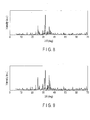
- the XRD patterns of these phosphors are sequentially shown in FIGS. 7 to 13 . Ten peaks selected from the XRD patterns in descending order of intensity were identified as the strongest peak. The diffraction angles (2 ⁇ ) were indicated by " ⁇ " in Table 4.
- any of the phosphors in the examples it is found that ten strongest peaks belong to any of diffraction angles (2 ⁇ ) of 15.05-15.15°, 23.03-23.13°, 24.87-24.97°, 25.7-25.8°, 25.97-26.07°, 29.33-29.43°, 30.92-31.02°, 31.65-31.75°, 31.88-31.98°, 33.02-33.12°, 33.59-33.69°, 34.35-34.45°, 35.2-35.3°, 36.02-36.12°, 36.55-36.65°, 37.3-37.4°, and 56.5-56.6°.
- the phosphors of Comparative Examples 1 and 2 were powders having a body color of yellow, and it was confirmed that the materials emitted yellow light when they were excited with black light. In the phosphors of these Comparative Examples, the 10 strongest peaks were not necessarily observed at the angles of diffraction (2 ⁇ ) described above.
- the aspect ratio and the luminescence property of the phosphors of Examples 2 to 8 and Comparative Examples 1 and 2 were found as described above. The results thereof were summarized in Table 5, together with the aspect ratio and the luminescence property of the phosphor of Example 1.
- the relative quantum efficiency is a relative intensity to the quantum efficiency of Example 4, which is 1, and it was obtained using an integrating sphere total luminous flux measuring device.
- x, y, z, u and w of any phosphor of Examples 1 to 8 are within the range described below. 0 ⁇ x ⁇ 1, 0.8 ⁇ y ⁇ 1.1, 2 ⁇ z ⁇ 3.5, 0 ⁇ u ⁇ 1 1.8 ⁇ z-u, 13 ⁇ u+w ⁇ 15
- the phosphors of Examples had the predetermined composition and the predetermined aspect ratio, and thus the materials can emit yellow light having a broad luminescence spectral half-width with a high efficiency.
- the Eu-activated orthosilicate phosphor (Comparative Example 3) had a narrow half-width of about 70 nm, and thus a light-emitting device having a good color rendering property cannot obtained even if it was combined with a blue light-emitting diode. Moreover, the brightness was remarkably reduced at high temperatures, and thus the efficiency is reduced in a high output light-emitting device to which power of about 300 mW or more is input.
- the phosphor having a good temperature property and capable of emitting yellow light having the broad spectral half-width can be provided with a high efficiency.
- the yellow-emitting phosphor of the present embodiment is combined with a blue LED, the white light-emitting device having the excellent color rendering property and the good luminescence property can be obtained.
Landscapes
- Chemical & Material Sciences (AREA)
- Engineering & Computer Science (AREA)
- Materials Engineering (AREA)
- Organic Chemistry (AREA)
- Ceramic Engineering (AREA)
- Inorganic Chemistry (AREA)
- Manufacturing & Machinery (AREA)
- Structural Engineering (AREA)
- Physics & Mathematics (AREA)
- Thermal Sciences (AREA)
- Led Device Packages (AREA)
- Luminescent Compositions (AREA)
Applications Claiming Priority (1)
| Application Number | Priority Date | Filing Date | Title |
|---|---|---|---|
| JP2013103400A JP2014224182A (ja) | 2013-05-15 | 2013-05-15 | 蛍光体、発光装置、および蛍光体の製造方法 |
Publications (1)
| Publication Number | Publication Date |
|---|---|
| EP2803714A1 true EP2803714A1 (fr) | 2014-11-19 |
Family
ID=50101815
Family Applications (1)
| Application Number | Title | Priority Date | Filing Date |
|---|---|---|---|
| EP14155376.8A Withdrawn EP2803714A1 (fr) | 2013-05-15 | 2014-02-17 | SiAlON:Ce luminophore |
Country Status (6)
| Country | Link |
|---|---|
| US (1) | US8957447B2 (fr) |
| EP (1) | EP2803714A1 (fr) |
| JP (1) | JP2014224182A (fr) |
| KR (1) | KR101603007B1 (fr) |
| CN (1) | CN104164231A (fr) |
| TW (1) | TW201500520A (fr) |
Cited By (1)
| Publication number | Priority date | Publication date | Assignee | Title |
|---|---|---|---|---|
| EP3286779A4 (fr) * | 2015-05-20 | 2019-02-06 | Nanophotonica, Inc. | Procédés pour améliorer le rendement de diodes électroluminescentes |
Families Citing this family (3)
| Publication number | Priority date | Publication date | Assignee | Title |
|---|---|---|---|---|
| JP2015157919A (ja) * | 2014-02-25 | 2015-09-03 | 株式会社東芝 | 蛍光体、発光装置、および蛍光体の製造方法 |
| JP2015187250A (ja) * | 2014-03-12 | 2015-10-29 | 株式会社東芝 | 蛍光体、その製造方法、およびその蛍光体を用いた発光装置 |
| WO2017051457A1 (fr) * | 2015-09-24 | 2017-03-30 | 株式会社 東芝 | Substance fluorescente, son procédé de production et dispositif électroluminescent comprenant ladite substance fluorescente |
Citations (3)
| Publication number | Priority date | Publication date | Assignee | Title |
|---|---|---|---|---|
| US20100164367A1 (en) * | 2007-05-22 | 2010-07-01 | Kousuke Shioi | Fluorescent substance, method for producing the same, and light-emitting device using the same |
| US20120104317A1 (en) * | 2005-09-27 | 2012-05-03 | Mitsubishi Chemical Corporation | Phosphor and manufacturing method therefore, and light emission device using the phosphor |
| US20120119234A1 (en) * | 2009-08-06 | 2012-05-17 | National Institute For Materials Science | Phosphor, method of manufacturing the same, and light-emitting device |
Family Cites Families (21)
| Publication number | Priority date | Publication date | Assignee | Title |
|---|---|---|---|---|
| MY149573A (en) * | 2002-10-16 | 2013-09-13 | Nichia Corp | Oxynitride phosphor and production process thereof, and light-emitting device using oxynitride phosphor |
| US7267787B2 (en) * | 2004-08-04 | 2007-09-11 | Intematix Corporation | Phosphor systems for a white light emitting diode (LED) |
| US7601276B2 (en) * | 2004-08-04 | 2009-10-13 | Intematix Corporation | Two-phase silicate-based yellow phosphor |
| US7524437B2 (en) * | 2005-03-04 | 2009-04-28 | Dowa Electronics Materials Co., Ltd. | Phosphor and manufacturing method of the same, and light emitting device using the phosphor |
| EP1867697B1 (fr) * | 2005-03-04 | 2014-05-14 | Mitsubishi Chemical Corporation | Substance fluorescente et procede de production de celle-ci, et dispositif d'emission de lumiere utilisant ladite substance fluorescente |
| US7443094B2 (en) * | 2005-03-31 | 2008-10-28 | Dowa Electronics Materials Co., Ltd. | Phosphor and manufacturing method of the same, and light emitting device using the phosphor |
| JP4975269B2 (ja) | 2005-04-28 | 2012-07-11 | Dowaホールディングス株式会社 | 蛍光体およびその製造方法、並びに当該蛍光体を用いた発光装置 |
| US8469760B2 (en) * | 2006-03-31 | 2013-06-25 | Dowa Electronics Materials Co., Ltd. | Light emitting device and method for producing same |
| KR100785492B1 (ko) * | 2006-04-17 | 2007-12-13 | 한국과학기술원 | 새로운 조성의 황색 발광 Ce3+부활 실리케이트황색형광체, 그 제조방법 및 상기 형광체를 포함하는 백색발광 다이오드 |
| KR100862695B1 (ko) * | 2006-10-17 | 2008-10-10 | 삼성전기주식회사 | 백색 발광 다이오드 |
| US8133461B2 (en) * | 2006-10-20 | 2012-03-13 | Intematix Corporation | Nano-YAG:Ce phosphor compositions and their methods of preparation |
| US8475683B2 (en) * | 2006-10-20 | 2013-07-02 | Intematix Corporation | Yellow-green to yellow-emitting phosphors based on halogenated-aluminates |
| TW200925250A (en) * | 2007-12-12 | 2009-06-16 | wei-hong Luo | Warm white light emitting semiconductor and yellow-orange silicate phosphor powder thereof |
| JP5592602B2 (ja) * | 2008-07-31 | 2014-09-17 | 株式会社東芝 | 蛍光体およびそれを用いた発光装置 |
| JP5754374B2 (ja) * | 2009-03-31 | 2015-07-29 | 三菱化学株式会社 | 蛍光体、蛍光体の製造方法、蛍光体含有組成物、発光装置、照明装置及び画像表示装置 |
| KR100963743B1 (ko) * | 2009-06-23 | 2010-06-14 | 한국광기술원 | 파장변환물질층을 구비하는 발광 다이오드 및 이의 제조방법 |
| US8178002B2 (en) * | 2009-12-21 | 2012-05-15 | Sabic Innovative Plastics Ip B.V. | Oxy-nitride pyrosilicate based persistent phosphors |
| JP5127965B2 (ja) * | 2010-09-02 | 2013-01-23 | 株式会社東芝 | 蛍光体およびそれを用いた発光装置 |
| JP5634352B2 (ja) * | 2011-08-24 | 2014-12-03 | 株式会社東芝 | 蛍光体、発光装置および蛍光体の製造方法 |
| JP5851214B2 (ja) * | 2011-11-16 | 2016-02-03 | 株式会社東芝 | 蛍光体、発光装置、および蛍光体の製造方法 |
| JP5762929B2 (ja) | 2011-11-16 | 2015-08-12 | 株式会社東芝 | 蛍光体、発光装置、および蛍光体の製造方法 |
-
2013
- 2013-05-15 JP JP2013103400A patent/JP2014224182A/ja active Pending
-
2014
- 2014-02-17 EP EP14155376.8A patent/EP2803714A1/fr not_active Withdrawn
- 2014-02-18 TW TW103105195A patent/TW201500520A/zh unknown
- 2014-02-21 CN CN201410060021.2A patent/CN104164231A/zh active Pending
- 2014-02-24 KR KR1020140021119A patent/KR101603007B1/ko not_active Ceased
- 2014-02-24 US US14/187,686 patent/US8957447B2/en not_active Expired - Fee Related
Patent Citations (3)
| Publication number | Priority date | Publication date | Assignee | Title |
|---|---|---|---|---|
| US20120104317A1 (en) * | 2005-09-27 | 2012-05-03 | Mitsubishi Chemical Corporation | Phosphor and manufacturing method therefore, and light emission device using the phosphor |
| US20100164367A1 (en) * | 2007-05-22 | 2010-07-01 | Kousuke Shioi | Fluorescent substance, method for producing the same, and light-emitting device using the same |
| US20120119234A1 (en) * | 2009-08-06 | 2012-05-17 | National Institute For Materials Science | Phosphor, method of manufacturing the same, and light-emitting device |
Non-Patent Citations (1)
| Title |
|---|
| "Space-group symmetry", vol. A, SPRINGER, article "International Tables for Crystallography" |
Cited By (2)
| Publication number | Priority date | Publication date | Assignee | Title |
|---|---|---|---|---|
| EP3286779A4 (fr) * | 2015-05-20 | 2019-02-06 | Nanophotonica, Inc. | Procédés pour améliorer le rendement de diodes électroluminescentes |
| US10593901B2 (en) | 2015-05-20 | 2020-03-17 | Nanophotonica, Inc. | Processes for improving efficiency of light emitting diodes |
Also Published As
| Publication number | Publication date |
|---|---|
| US20140339583A1 (en) | 2014-11-20 |
| KR101603007B1 (ko) | 2016-03-11 |
| KR20140135091A (ko) | 2014-11-25 |
| TW201500520A (zh) | 2015-01-01 |
| JP2014224182A (ja) | 2014-12-04 |
| US8957447B2 (en) | 2015-02-17 |
| CN104164231A (zh) | 2014-11-26 |
Similar Documents
| Publication | Publication Date | Title |
|---|---|---|
| US9133391B2 (en) | Luminescent material | |
| JP5129283B2 (ja) | 蛍光体、蛍光体の製造方法、発光装置及び発光モジュール | |
| US20160087163A1 (en) | Phosphor, method for producing the same, and light-emitting device using the same | |
| EP2915862A1 (fr) | Phosphore et procédé de production de phosphore et dispositif électroluminescent l'utilisant | |
| US8957447B2 (en) | Phosphor | |
| EP2778211A1 (fr) | Phosphore et dispositif électroluminescent l'utilisant | |
| KR101451016B1 (ko) | 발광 물질 | |
| EP2781576A1 (fr) | Luminophore, dispositif électroluminescent et procédé de production de ce phosphore | |
| EP2803716B1 (fr) | Sialon luminophore | |
| EP2918654A2 (fr) | Phosphore, procédé de production de celui-ci et dispositif électroluminescent utilisant celui-ci | |
| JP6546304B2 (ja) | 蛍光体および発光装置 | |
| JP2016056241A (ja) | 蛍光体、その製造方法、およびその蛍光体を用いた発光装置 | |
| EP2999015A1 (fr) | Phosphore, dispositif électroluminescent et procédé de production de ce phosphore | |
| US20160083648A1 (en) | Phosphor, method for producing the same, and light-emitting device using the same |
Legal Events
| Date | Code | Title | Description |
|---|---|---|---|
| PUAI | Public reference made under article 153(3) epc to a published international application that has entered the european phase |
Free format text: ORIGINAL CODE: 0009012 |
|
| 17P | Request for examination filed |
Effective date: 20140217 |
|
| AK | Designated contracting states |
Kind code of ref document: A1 Designated state(s): AL AT BE BG CH CY CZ DE DK EE ES FI FR GB GR HR HU IE IS IT LI LT LU LV MC MK MT NL NO PL PT RO RS SE SI SK SM TR |
|
| AX | Request for extension of the european patent |
Extension state: BA ME |
|
| 17Q | First examination report despatched |
Effective date: 20151002 |
|
| RIC1 | Information provided on ipc code assigned before grant |
Ipc: H01L 33/50 20100101ALN20160107BHEP Ipc: C09K 11/08 20060101AFI20160107BHEP Ipc: C09K 11/77 20060101ALI20160107BHEP |
|
| GRAP | Despatch of communication of intention to grant a patent |
Free format text: ORIGINAL CODE: EPIDOSNIGR1 |
|
| RIC1 | Information provided on ipc code assigned before grant |
Ipc: C09K 11/77 20060101ALI20160323BHEP Ipc: H01L 33/50 20100101ALN20160323BHEP Ipc: C09K 11/08 20060101AFI20160323BHEP |
|
| INTG | Intention to grant announced |
Effective date: 20160413 |
|
| STAA | Information on the status of an ep patent application or granted ep patent |
Free format text: STATUS: THE APPLICATION IS DEEMED TO BE WITHDRAWN |
|
| 18D | Application deemed to be withdrawn |
Effective date: 20160824 |