EP2804067A1 - Régulateur de tension LDO à faible puissance et bruit de sortie à faible densité - Google Patents
Régulateur de tension LDO à faible puissance et bruit de sortie à faible densité Download PDFInfo
- Publication number
- EP2804067A1 EP2804067A1 EP20130305645 EP13305645A EP2804067A1 EP 2804067 A1 EP2804067 A1 EP 2804067A1 EP 20130305645 EP20130305645 EP 20130305645 EP 13305645 A EP13305645 A EP 13305645A EP 2804067 A1 EP2804067 A1 EP 2804067A1
- Authority
- EP
- European Patent Office
- Prior art keywords
- voltage
- circuit
- band
- output
- stage
- Prior art date
- Legal status (The legal status is an assumption and is not a legal conclusion. Google has not performed a legal analysis and makes no representation as to the accuracy of the status listed.)
- Granted
Links
- 230000001105 regulatory effect Effects 0.000 claims abstract description 28
- 239000003990 capacitor Substances 0.000 claims abstract description 15
- 238000010586 diagram Methods 0.000 description 8
- XUIMIQQOPSSXEZ-UHFFFAOYSA-N Silicon Chemical compound [Si] XUIMIQQOPSSXEZ-UHFFFAOYSA-N 0.000 description 5
- 229910052710 silicon Inorganic materials 0.000 description 5
- 239000010703 silicon Substances 0.000 description 5
- 238000013459 approach Methods 0.000 description 3
- 230000000295 complement effect Effects 0.000 description 2
- 230000000694 effects Effects 0.000 description 2
- 238000005516 engineering process Methods 0.000 description 2
- 230000010354 integration Effects 0.000 description 2
- 238000012986 modification Methods 0.000 description 2
- 230000004048 modification Effects 0.000 description 2
- 230000015556 catabolic process Effects 0.000 description 1
- 230000001276 controlling effect Effects 0.000 description 1
- 230000008878 coupling Effects 0.000 description 1
- 238000010168 coupling process Methods 0.000 description 1
- 238000005859 coupling reaction Methods 0.000 description 1
- 238000006731 degradation reaction Methods 0.000 description 1
- 230000014509 gene expression Effects 0.000 description 1
- 239000000758 substrate Substances 0.000 description 1
Images


Classifications
-
- G—PHYSICS
- G05—CONTROLLING; REGULATING
- G05F—SYSTEMS FOR REGULATING ELECTRIC OR MAGNETIC VARIABLES
- G05F1/00—Automatic systems in which deviations of an electric quantity from one or more predetermined values are detected at the output of the system and fed back to a device within the system to restore the detected quantity to its predetermined value or values, i.e. retroactive systems
- G05F1/10—Regulating voltage or current
- G05F1/46—Regulating voltage or current wherein the variable actually regulated by the final control device is DC
- G05F1/56—Regulating voltage or current wherein the variable actually regulated by the final control device is DC using semiconductor devices in series with the load as final control devices
- G05F1/575—Regulating voltage or current wherein the variable actually regulated by the final control device is DC using semiconductor devices in series with the load as final control devices characterised by the feedback circuit
Definitions
- the present invention generally relates to Low-Dropout (LDO) voltage regulators used in the design of Integrated Circuits (IC), and more particularly to such regulators having low output noise density and low internal power consumption.
- LDO Low-Dropout
- LDO regulators work in the same way as all linear voltage regulators.
- LDO regulators utilize open collector or open drain output transistor (also named “pass transistor”), instead of the emitter follower pass transistor used in non-LDO regulators.
- the output transistor of LDO regulators operates in the saturation range. The result which is achieved is that the voltage drop from the unregulated voltage to the regulated voltage can be as low as the saturation voltage across the output transistor.
- LDO voltage regulators are characterized by their low drop-out voltage.
- a LDO regulator should provide a regulated voltage with a very low output noise density while limiting the internal power consumption.
- Integrated capacitors may be used to stabilize the structure, because a strong current is necessary to obtain low noise output voltage. Consequently, the size of the LDO is strongly increased.
- Reference EP1624357 discloses a typical LDO voltage regulator topology, which uses a band-gap reference voltage generator, a comparator, and a power output stage. These three elements are independent of each other, with only one return path from the output stage to one of the comparator inputs.
- the output stage comprises a resistor voltage divider for generating a feedback voltage for the return path.
- the band-gap reference voltage generator can have a single Vbe structure or a double Vbe structure. Despite some performance limits, such structures are very simple to implement to provide regulated voltages independent of temperature. A lot of variants of this type of LDO regulator are available. Some are described in further prior art references such as EP0715238 , EP1336912 , and EP1865397 .
- Such enhancement consists in using a filter on the reference voltage or in the return path. Being controlled by the output stage, this filter can ensure good noise attenuation while not jeopardizing the stability of the system.
- This filter can be an active filter, suitable for compensating, in particular, noise from the power supply.
- Still other structures include two integrated band-gap reference voltage generators.
- One generator exhibits a double Vbe structure and is adapted to provide low noise current, while the other has a single Vbe structure and ensures the regulated output voltage reference. This allows very low noise voltage with strong stability at the cost, however, of a high complexity and thus wide silicon area.
- Double Vbe band-gap structures also known as "stacked Vbe band-gap" structures
- Double Vbe band-gap structures have become widely used to get very low noise and temperature compensated output voltage LDOs.
- such structure provides an output voltage regulated corresponding only to a multiple of band gap voltage, namely k ⁇ Vbg where k is an integral number.
- additional integrated capacitors may be needed to stabilize the structure because a strong current is necessary to obtain low noise output voltage. Consequently the size of the LDO is strongly increased.
- a first aspect of the present invention relates to a low drop-out voltage regulating circuit comprising, arranged in parallel between a first power supply node and a second power supply node:
- the circuit has a first feedback DC loop adapted to set the current in the band-gap reference stage, in order to provide low noise and temperature compensation.
- the circuit further comprises a second feedback DC loop adapted to control the pass device of the output stage, in order to provide low drop-out regulated voltage at the output of the circuit.
- the first and second feedback DC loops are independent one from the other and operate simultaneously. The stability can be ensured by a single capacitor at the output of the circuit, which may be external to the circuit..
- the controlled output voltage can be tuned from almost the supply voltage down to one time the band-gap voltage ( Vbg ), e.g. approximately 1.2 volt (V), with temperature compensation.
- Vbg band-gap voltage
- the proposed structure provides very low noise regulated voltage with a high integration level of components compared to typical regulator structures
- Output capacitor provides good stability to the system and double Vbe structure provides low noise. No additional filter is required on the reference voltage, nor in the feedback loop.
- a second aspect of the present invention relates to an integrated circuit comprising a low dropout voltage regulating circuit according to the first aspect.
- the circuit may be, for instance, a frequency synthesizer, a Digital-to-Analog Converter (DAC), a radiofrequency modulator, a power amplifier, etc.
- DAC Digital-to-Analog Converter
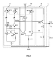
- FIG.1 there is shown therein a schematic diagram of an embodiment of a low drop-out (LDO) voltage regulating circuit 1 according to embodiments of the present invention.
- LDO low drop-out
- the circuit 1 may be part of an Integrated Circuit (IC) chip.
- the chip may be, for instance, a frequency synthesizer, a Digital-to-Analog Converter (DAC), a radiofrequency modulator, a power amplifier, etc. It will be appreciated that this list is non exhaustive. Such chips are used, e.g., in radio and television sets, portable telephone, and more generally all wireless applications.
- IC Integrated Circuit
- the LDO regulator 1 mainly comprises first, second and third stages 10, 20 and 30, respectively. Stages 10, 20 and 30 are arranged in parallel between a first power supply node receiving a high supply voltage VDD and a second power supply node receiving a low supply voltage or the ground GND as shown. These nodes may be coupled to respective terminals of the IC, e.g. for receiving the high supply voltage from the exterior of the IC.
- the LDO regulator is operable to generate a regulated output voltage Vout at an output node 2 of the circuit, which is independent of the current sunk by a load (not shown) which can be coupled to said output node 2, and which is not or little sensitive to variations of the high power supply VDD and of temperature.
- an output device is controlled by control circuitry to provide the required voltage level for a wide range of current sunk by the load, as required by the application.
- stage 10 typically comprises a reference voltage generator having band-gap architecture, hereinafter referred to as the band-gap reference stage or band-gap reference.
- the reference voltage generator is a so called “double Vbe " band-gap reference adapted to provide a first reference voltage Vbg and a second band-gap reference voltage 2xVbg , where Vbg is substantially equal to the silicon band-gap voltage.
- the band-gap voltage reference circuit comprises first and second branches respectively including first and second groups of transistors of different emitter current conduction areas, and current sources for running the first and second groups of transistors at different emitter current densities to generate respective base-emitter voltages.
- the branches of the double Vbe band-gap reference comprises transistors BN5 and BN6, respectively, for instance bipolar transistors, e.g. of the N conduction type (i.e., NPN transistors).
- the respective base of BN5 and BN6 are coupled one to each other, and to the collector of BN6.
- the emitter of BN5 is coupled to the ground GND through a first resistor R1 and a second resistor R2 in series.
- the emitter of BN6 is coupled to the ground GND directly (namely not through R1) through the second resistor R2.
- a pair of cross-coupled transistors BN3 and BN4 of the same type as BN5 and BN6 is inserted between resistors R1 and R2 one hand, and transistors BN5 and BN6 on the other hand. More precisely, transistors BN3 and BN4 are so arranged that the emitter-collector path of BN3 is inserted between the emitter of BN5 and resistor R1, and the emitter-collector path of BN4 is inserted between the emitter of BN6 and resistor R2. In addition, the base of BN3 is coupled to the collector of BN4, and vice versa.
- the collector of BN5 is coupled to VDD through e.g. a MOS transistor MP4 of the P type (or PMOS), and the collector of BN6 is coupled to VDD through e.g. a PMOS transistor MP5.
- MP4 and MP5 have a respective transistor size (length/width) of n and m , respectively, where m is different from n .
- the transistors MP4 and MP5 have their respective gates coupled one to each other. The current I0 and I1 in their respective branches are thus different one form the other.
- the transistors may be designed so that m > n .
- m and n may be selected so that, approximately, m equals twice n ( m ⁇ 2n ). This allows saving current consumption in the IC.
- the resulting voltage Vbg at the collector of BN4 is about 1.2-1.3 V, depending on the particular technology and circuit design, and is close to the theoretical 1.22 V band-gap of silicon at a temperature of 0 K. Further, the resulting voltage at the collector of BN5 is 2xVbg. The remaining voltage change over the operating temperature of typical integrated circuits is on the order of a few millivolts only.
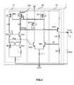
- the band-gap reference 10 is controlled by a regulation error amplifier of the second stage 20, as will be described in more details below with reference to FIG.3 .
- the second stage 20 indeed, comprises a differential transistor pair operable as a voltage comparator.
- the differential transistor pair comprises first and second transistors BN1 and BN2, respectively, for example bipolar transistors, e.g. of the N-conduction type (NPN transistors).
- the common emitters of BN1 and BN2 are coupled to the ground GND through a resistor Rdiff.
- the differential pair is biased by a PTAT current Idiff matched with the band-gap current of the reference stage 10.
- the collector of BN1 is coupled to VDD through a diode-connected transistor MP3, for instance a MOS transistor of e.g. P-conductivity type.
- MP3 is connected as a diode, having its base connected to its gate.
- the gate of MP3 is further connected to the gate of transistors MP4 and MP5 of the first stage 10, whereby these three transistors are current-mirrored. These elements form current regulation means for the reference stage 10.
- the collector of BN2 is coupled to VDD through a transistor MP2, for example a transistor of same type as MP3, namely a PMOS transistor in the shown example.
- MP3 has the same size (length/width) p as MP3. What is achieved is that the two branches of the comparator stage 20 operate under the same DC conditions, and thus the comparator is well balanced.
- the comparator stage 20 receives reference voltage Vbg from the reference stage 10 and a feedback voltage Vf from the output stage 30. More precisely, voltages Vbg and Vf are provided to the base terminals of transistors BN2 and BN1 respectively, of the comparator 20.
- comparator 20 provides a control signal back to the band-gap reference generator 10 through transistors BN1, MP3, MP4 and MP5, as will be further explicated below with reference to FIG.2 , such that the feedback voltage Vf equals the first reference voltage Vbg , resulting in the required output voltage Vout.
- This control signal operates by modifying current I0 in the branch of the band-gap reference stage 10 which comprises transistor BN6.
- comparator 20 provides another control signal back to the band-gap reference generator 10 through transistors BN1, MP3 and MP4, as will be further explicated below with reference to FIG.3 .
- This control signal operates by modifying current I1 in the branch of the band-gap reference stage 10 which comprises transistor BN5.
- the above element constitute a first DC regulation loop and a second DC regulation loop, respectively which provide enhanced voltage regulation, as will become more apparent from the remaining of the present description.
- the output or buffer stage is adapted to generate the regulated output voltage Vout. To that end, it comprises a pass device.
- the pass device comprises a transistor, for exempla a MOS transistor MP1 of e.g. the P conductivity type (i.e., a PMOS transistor).
- the source of MP1 is coupled to VDD, for example through a direct connection, and its drain is connected to the output node 2 in order to drive current to the load.
- the pass device may be coupled to a large bypass (or decoupling) capacitor Cstab, connected through the output node 2 and the ground.
- the value of capacitor Cstab is selected so as to provide stability of the output voltage Vout over a wide range of load current changes.
- capacitor Cstab may be an external capacitor of, for example, a few hundreds nanofarads (nF), e.g. 100 nF.
- the output stage 30 further comprises means to feed an image of the output Voltage back to the error amplifier of the comparator stage 20.
- feedback is achieved by a voltage divider operable to generate the feedback voltage Vf .
- the voltage divider may comprise first and second resistors R3 and R4, respectively, arranged in series between the output node 2 and the ground GND. The node between resistors R3 and R4 is coupled to the base of transistor BN1 of the differential transistor pair of the comparator stage 20, to provide a voltage indicative of the actual output voltage Vout.
- resistors R3 and R4 are selected so as to be sufficiently high to avoid deviating too much current from the output node 2 to the ground GND, in other to save current consumption.
- the pass transistor MP1 is controlled by the reference voltage generator 10. More precisely, the gate of MP1 is coupled to the band-gap generator for receiving the second band-gap voltage 2xVbg from the collector of transistor BN5. For example, this coupling comprises a direct connection, as shown in FIG.1 .
- LDO regulator is controlled by two independent feedback DC loops operating simultaneously.
- a first loop sets the current I0 in the band-gap reference stage 10 to provide low noise and temperature compensation.
- the second loop controls the pass device MP1 of an output stage 30 to provide low drop-out regulated voltage Vout at the output 2 of the circuit.
- the stability is ensured by a single capacitor Cstab at the output of the circuit, which may be external to the circuit.
- a first feedback DC loop 100 is adapted to set the current I0 in the band-gap reference stage 10, in order to provide low noise and temperature compensation.
- Loop 100 starts from the differential transistor pair BN1, BN2. Any error current flowing through the collector of BN1 is copied through mirrored transistors MP3 and MP5 with the effect that I0 is modified in order to cancel the error by modifying the band-gap voltage Vbg on the base of BN2. This feedback operates until the unbalance between both branches of the differential transistor pair is cancelled.
- a second feedback DC loop 200 is adapted to control gate of the pass device MP1 of the output stage 30, in order to provide low drop-out regulated voltage Vout at the output 2 of the circuit.
- the loop 200 Starting from the output node 2, the loop 200 generates the image voltage Vf of the output voltage which, through transistors BN1, MP3 and MP4 is operable to cause the current I1 to increase when voltage Vout drifts.
- the two DC feedback loops have some path portions in common. Indeed, they both use some part of the current regulating means comprising PMOS transistors MP3, MP4 and MP5.
- the ratio I0/I1 does not depend on n , the size (width/length) of transistor MP4.
- I1 does not vary when I0 varies as a function of temperature due to the DC feedback loop 100.
- I1 can vary as a function of the current sunk by the load due to the DC feedback loop 200.
- the DC feedback loops are independent one from each other.
- the proposed architecture of which embodiments have been described above is an ultra-low noise and low power LDO based on a double band-gap reference structure.
- This system has the capability to provide regulated output voltage down to one Vbg. More precisely, the controlled output voltage Vout can be tuned from almost the supply voltage VDD down to Vbg, i.e. approximately 1.2 V.
- integrated capacitors are not needed to ensure the stability of the system (only one external capacitor at the output).
- the circuit 1 is implemented in a submicron CMOS technology, but this is not limitative.
- the pass device and current regulating means comprise MOS transistors, for example MOSFETs.
- MOS transistors for example MOSFETs.
- bipolar transistors, JFETs, etc. can be used as well.
- one or more small integrated capacitors could be provided at the output of the LDO circuit for providing further voltage fluctuation compensation.
- comparator structure could also be used in replacement of the simple differential pair of the comparator stage 20 as shown.
Landscapes
- Engineering & Computer Science (AREA)
- Physics & Mathematics (AREA)
- Electromagnetism (AREA)
- General Physics & Mathematics (AREA)
- Radar, Positioning & Navigation (AREA)
- Automation & Control Theory (AREA)
- Continuous-Control Power Sources That Use Transistors (AREA)
Priority Applications (1)
| Application Number | Priority Date | Filing Date | Title |
|---|---|---|---|
| EP13305645.7A EP2804067B1 (fr) | 2013-05-17 | 2013-05-17 | Régulateur de tension LDO à faible puissance et bruit de sortie à faible densité |
Applications Claiming Priority (1)
| Application Number | Priority Date | Filing Date | Title |
|---|---|---|---|
| EP13305645.7A EP2804067B1 (fr) | 2013-05-17 | 2013-05-17 | Régulateur de tension LDO à faible puissance et bruit de sortie à faible densité |
Publications (2)
| Publication Number | Publication Date |
|---|---|
| EP2804067A1 true EP2804067A1 (fr) | 2014-11-19 |
| EP2804067B1 EP2804067B1 (fr) | 2015-12-09 |
Family
ID=48570032
Family Applications (1)
| Application Number | Title | Priority Date | Filing Date |
|---|---|---|---|
| EP13305645.7A Not-in-force EP2804067B1 (fr) | 2013-05-17 | 2013-05-17 | Régulateur de tension LDO à faible puissance et bruit de sortie à faible densité |
Country Status (1)
| Country | Link |
|---|---|
| EP (1) | EP2804067B1 (fr) |
Cited By (5)
| Publication number | Priority date | Publication date | Assignee | Title |
|---|---|---|---|---|
| CN106843363A (zh) * | 2017-03-06 | 2017-06-13 | 重庆湃芯微电子有限公司 | 一种带隙基准电路中的不使用倒比管的反馈式启动电路 |
| US10033270B2 (en) | 2016-10-26 | 2018-07-24 | International Business Machines Corporation | Dynamic voltage regulation |
| US10069409B2 (en) | 2016-09-13 | 2018-09-04 | International Business Machines Corporation | Distributed voltage regulation system for mitigating the effects of IR-drop |
| EP3514653A1 (fr) * | 2018-01-19 | 2019-07-24 | Socionext Inc. | Circuit de génération de signal |
| CN111474974A (zh) * | 2020-04-30 | 2020-07-31 | 上海维安半导体有限公司 | 一种提高ldo由重载突变到轻载或空载时瞬态响应的方法 |
Families Citing this family (1)
| Publication number | Priority date | Publication date | Assignee | Title |
|---|---|---|---|---|
| CN106774582B (zh) * | 2017-02-13 | 2018-11-09 | 许昌学院 | 一种应用于生物体植入系统的电源电路 |
Citations (11)
| Publication number | Priority date | Publication date | Assignee | Title |
|---|---|---|---|---|
| US5325045A (en) * | 1993-02-17 | 1994-06-28 | Exar Corporation | Low voltage CMOS bandgap with new trimming and curvature correction methods |
| EP0715238A2 (fr) | 1994-12-01 | 1996-06-05 | Texas Instruments Incorporated | Circuit et méthode pour la régulation d'une tension |
| EP1191416A2 (fr) | 2000-09-20 | 2002-03-27 | Texas Instruments Inc. | Régulateur de tension |
| EP1229419A2 (fr) | 2001-02-02 | 2002-08-07 | Broadcom Corporation | Régulateur à faible chute de tension, taux élevé de réjection du bruit d'alimentation et largeur de bande élevée |
| EP1336912A1 (fr) | 2002-02-18 | 2003-08-20 | Motorola, Inc. | Régulateur de tension à faible tension de déchêt |
| EP1365302A1 (fr) | 2002-05-20 | 2003-11-26 | Texas Instruments Incorporated | Régulateur à faible perte de tension |
| EP1624357A1 (fr) | 2004-08-06 | 2006-02-08 | Nanopower Solution Co., Ltd. | Régulateur de tension avec moyens de commande inverse adaptatives |
| US7030598B1 (en) | 2003-08-06 | 2006-04-18 | National Semiconductor Corporation | Low dropout voltage regulator |
| EP1865397A1 (fr) | 2006-06-05 | 2007-12-12 | St Microelectronics S.A. | Régulateur de tension à faible chute |
| US7362081B1 (en) | 2005-02-02 | 2008-04-22 | National Semiconductor Corporation | Low-dropout regulator |
| CN102681584A (zh) * | 2012-05-30 | 2012-09-19 | 昆山锐芯微电子有限公司 | 低噪声带隙基准电路和基准源产生系统 |
-
2013
- 2013-05-17 EP EP13305645.7A patent/EP2804067B1/fr not_active Not-in-force
Patent Citations (11)
| Publication number | Priority date | Publication date | Assignee | Title |
|---|---|---|---|---|
| US5325045A (en) * | 1993-02-17 | 1994-06-28 | Exar Corporation | Low voltage CMOS bandgap with new trimming and curvature correction methods |
| EP0715238A2 (fr) | 1994-12-01 | 1996-06-05 | Texas Instruments Incorporated | Circuit et méthode pour la régulation d'une tension |
| EP1191416A2 (fr) | 2000-09-20 | 2002-03-27 | Texas Instruments Inc. | Régulateur de tension |
| EP1229419A2 (fr) | 2001-02-02 | 2002-08-07 | Broadcom Corporation | Régulateur à faible chute de tension, taux élevé de réjection du bruit d'alimentation et largeur de bande élevée |
| EP1336912A1 (fr) | 2002-02-18 | 2003-08-20 | Motorola, Inc. | Régulateur de tension à faible tension de déchêt |
| EP1365302A1 (fr) | 2002-05-20 | 2003-11-26 | Texas Instruments Incorporated | Régulateur à faible perte de tension |
| US7030598B1 (en) | 2003-08-06 | 2006-04-18 | National Semiconductor Corporation | Low dropout voltage regulator |
| EP1624357A1 (fr) | 2004-08-06 | 2006-02-08 | Nanopower Solution Co., Ltd. | Régulateur de tension avec moyens de commande inverse adaptatives |
| US7362081B1 (en) | 2005-02-02 | 2008-04-22 | National Semiconductor Corporation | Low-dropout regulator |
| EP1865397A1 (fr) | 2006-06-05 | 2007-12-12 | St Microelectronics S.A. | Régulateur de tension à faible chute |
| CN102681584A (zh) * | 2012-05-30 | 2012-09-19 | 昆山锐芯微电子有限公司 | 低噪声带隙基准电路和基准源产生系统 |
Cited By (7)
| Publication number | Priority date | Publication date | Assignee | Title |
|---|---|---|---|---|
| US10069409B2 (en) | 2016-09-13 | 2018-09-04 | International Business Machines Corporation | Distributed voltage regulation system for mitigating the effects of IR-drop |
| US10033270B2 (en) | 2016-10-26 | 2018-07-24 | International Business Machines Corporation | Dynamic voltage regulation |
| CN106843363A (zh) * | 2017-03-06 | 2017-06-13 | 重庆湃芯微电子有限公司 | 一种带隙基准电路中的不使用倒比管的反馈式启动电路 |
| CN106843363B (zh) * | 2017-03-06 | 2018-01-02 | 重庆湃芯微电子有限公司 | 一种带隙基准电路中的不使用倒比管的反馈式启动电路 |
| EP3514653A1 (fr) * | 2018-01-19 | 2019-07-24 | Socionext Inc. | Circuit de génération de signal |
| US10671104B2 (en) | 2018-01-19 | 2020-06-02 | Socionext Inc. | Signal generation circuitry |
| CN111474974A (zh) * | 2020-04-30 | 2020-07-31 | 上海维安半导体有限公司 | 一种提高ldo由重载突变到轻载或空载时瞬态响应的方法 |
Also Published As
| Publication number | Publication date |
|---|---|
| EP2804067B1 (fr) | 2015-12-09 |
Similar Documents
| Publication | Publication Date | Title |
|---|---|---|
| US7656145B2 (en) | Low power bandgap voltage reference circuit having multiple reference voltages with high power supply rejection ratio | |
| US6259238B1 (en) | Brokaw transconductance operational transconductance amplifier-based micropower low drop out voltage regulator having counterphase compensation | |
| US7705662B2 (en) | Low voltage high-output-driving CMOS voltage reference with temperature compensation | |
| US6005378A (en) | Compact low dropout voltage regulator using enhancement and depletion mode MOS transistors | |
| EP2804067B1 (fr) | Régulateur de tension LDO à faible puissance et bruit de sortie à faible densité | |
| US7023181B2 (en) | Constant voltage generator and electronic equipment using the same | |
| CN108958348A (zh) | 一种高电源抑制比的带隙基准源 | |
| US8269478B2 (en) | Two-terminal voltage regulator with current-balancing current mirror | |
| US20090295360A1 (en) | Start-Up Circuit and Method for a Self-Biased Zero-Temperature-Coefficient Current Reference | |
| US10671104B2 (en) | Signal generation circuitry | |
| US4906863A (en) | Wide range power supply BiCMOS band-gap reference voltage circuit | |
| US7872462B2 (en) | Bandgap reference circuits | |
| EP1229420A1 (fr) | Référence de tension du type bande interdite à basse tension d'alimentation | |
| US11762410B2 (en) | Voltage reference with temperature-selective second-order temperature compensation | |
| Ng et al. | A Sub-1 V, 26$\mu $ W, Low-Output-Impedance CMOS Bandgap Reference With a Low Dropout or Source Follower Mode | |
| KR100930275B1 (ko) | 씨모스를 이용한 밴드갭 레퍼런스 발생기 | |
| US8222884B2 (en) | Reference voltage generator with bootstrapping effect | |
| US11353910B1 (en) | Bandgap voltage regulator | |
| US6118263A (en) | Current generator circuitry with zero-current shutdown state | |
| WO2001020419A1 (fr) | Dispositif a semi-conducteur | |
| US20080001592A1 (en) | Method for generating a reference current and a related feedback generator | |
| US20090096438A1 (en) | Voltage control circuit | |
| US6998830B1 (en) | Band-gap reference | |
| US6175226B1 (en) | Differential amplifier with common-mode regulating circuit | |
| Galang et al. | Development of low power low dropout regulator with temperature and voltage protection schemes for wireless sensor network application |
Legal Events
| Date | Code | Title | Description |
|---|---|---|---|
| PUAI | Public reference made under article 153(3) epc to a published international application that has entered the european phase |
Free format text: ORIGINAL CODE: 0009012 |
|
| 17P | Request for examination filed |
Effective date: 20140702 |
|
| AK | Designated contracting states |
Kind code of ref document: A1 Designated state(s): AL AT BE BG CH CY CZ DE DK EE ES FI FR GB GR HR HU IE IS IT LI LT LU LV MC MK MT NL NO PL PT RO RS SE SI SK SM TR |
|
| AX | Request for extension of the european patent |
Extension state: BA ME |
|
| GRAP | Despatch of communication of intention to grant a patent |
Free format text: ORIGINAL CODE: EPIDOSNIGR1 |
|
| INTG | Intention to grant announced |
Effective date: 20150518 |
|
| GRAR | Information related to intention to grant a patent recorded |
Free format text: ORIGINAL CODE: EPIDOSNIGR71 |
|
| GRAS | Grant fee paid |
Free format text: ORIGINAL CODE: EPIDOSNIGR3 |
|
| GRAA | (expected) grant |
Free format text: ORIGINAL CODE: 0009210 |
|
| INTG | Intention to grant announced |
Effective date: 20151016 |
|
| AK | Designated contracting states |
Kind code of ref document: B1 Designated state(s): AL AT BE BG CH CY CZ DE DK EE ES FI FR GB GR HR HU IE IS IT LI LT LU LV MC MK MT NL NO PL PT RO RS SE SI SK SM TR |
|
| REG | Reference to a national code |
Ref country code: GB Ref legal event code: FG4D |
|
| REG | Reference to a national code |
Ref country code: AT Ref legal event code: REF Ref document number: 764843 Country of ref document: AT Kind code of ref document: T Effective date: 20151215 Ref country code: CH Ref legal event code: EP |
|
| REG | Reference to a national code |
Ref country code: IE Ref legal event code: FG4D |
|
| REG | Reference to a national code |
Ref country code: DE Ref legal event code: R096 Ref document number: 602013004109 Country of ref document: DE |
|
| REG | Reference to a national code |
Ref country code: LT Ref legal event code: MG4D |
|
| REG | Reference to a national code |
Ref country code: NL Ref legal event code: MP Effective date: 20151209 |
|
| PG25 | Lapsed in a contracting state [announced via postgrant information from national office to epo] |
Ref country code: LT Free format text: LAPSE BECAUSE OF FAILURE TO SUBMIT A TRANSLATION OF THE DESCRIPTION OR TO PAY THE FEE WITHIN THE PRESCRIBED TIME-LIMIT Effective date: 20151209 Ref country code: ES Free format text: LAPSE BECAUSE OF FAILURE TO SUBMIT A TRANSLATION OF THE DESCRIPTION OR TO PAY THE FEE WITHIN THE PRESCRIBED TIME-LIMIT Effective date: 20151209 Ref country code: NO Free format text: LAPSE BECAUSE OF FAILURE TO SUBMIT A TRANSLATION OF THE DESCRIPTION OR TO PAY THE FEE WITHIN THE PRESCRIBED TIME-LIMIT Effective date: 20160309 |
|
| REG | Reference to a national code |
Ref country code: AT Ref legal event code: MK05 Ref document number: 764843 Country of ref document: AT Kind code of ref document: T Effective date: 20151209 |
|
| PG25 | Lapsed in a contracting state [announced via postgrant information from national office to epo] |
Ref country code: NL Free format text: LAPSE BECAUSE OF FAILURE TO SUBMIT A TRANSLATION OF THE DESCRIPTION OR TO PAY THE FEE WITHIN THE PRESCRIBED TIME-LIMIT Effective date: 20151209 Ref country code: RS Free format text: LAPSE BECAUSE OF FAILURE TO SUBMIT A TRANSLATION OF THE DESCRIPTION OR TO PAY THE FEE WITHIN THE PRESCRIBED TIME-LIMIT Effective date: 20151209 Ref country code: LV Free format text: LAPSE BECAUSE OF FAILURE TO SUBMIT A TRANSLATION OF THE DESCRIPTION OR TO PAY THE FEE WITHIN THE PRESCRIBED TIME-LIMIT Effective date: 20151209 Ref country code: GR Free format text: LAPSE BECAUSE OF FAILURE TO SUBMIT A TRANSLATION OF THE DESCRIPTION OR TO PAY THE FEE WITHIN THE PRESCRIBED TIME-LIMIT Effective date: 20160310 Ref country code: SE Free format text: LAPSE BECAUSE OF FAILURE TO SUBMIT A TRANSLATION OF THE DESCRIPTION OR TO PAY THE FEE WITHIN THE PRESCRIBED TIME-LIMIT Effective date: 20151209 Ref country code: FI Free format text: LAPSE BECAUSE OF FAILURE TO SUBMIT A TRANSLATION OF THE DESCRIPTION OR TO PAY THE FEE WITHIN THE PRESCRIBED TIME-LIMIT Effective date: 20151209 |
|
| PG25 | Lapsed in a contracting state [announced via postgrant information from national office to epo] |
Ref country code: IS Free format text: LAPSE BECAUSE OF FAILURE TO SUBMIT A TRANSLATION OF THE DESCRIPTION OR TO PAY THE FEE WITHIN THE PRESCRIBED TIME-LIMIT Effective date: 20151209 |
|
| PG25 | Lapsed in a contracting state [announced via postgrant information from national office to epo] |
Ref country code: CZ Free format text: LAPSE BECAUSE OF FAILURE TO SUBMIT A TRANSLATION OF THE DESCRIPTION OR TO PAY THE FEE WITHIN THE PRESCRIBED TIME-LIMIT Effective date: 20151209 Ref country code: IT Free format text: LAPSE BECAUSE OF FAILURE TO SUBMIT A TRANSLATION OF THE DESCRIPTION OR TO PAY THE FEE WITHIN THE PRESCRIBED TIME-LIMIT Effective date: 20151209 |
|
| PG25 | Lapsed in a contracting state [announced via postgrant information from national office to epo] |
Ref country code: SK Free format text: LAPSE BECAUSE OF FAILURE TO SUBMIT A TRANSLATION OF THE DESCRIPTION OR TO PAY THE FEE WITHIN THE PRESCRIBED TIME-LIMIT Effective date: 20151209 Ref country code: AT Free format text: LAPSE BECAUSE OF FAILURE TO SUBMIT A TRANSLATION OF THE DESCRIPTION OR TO PAY THE FEE WITHIN THE PRESCRIBED TIME-LIMIT Effective date: 20151209 Ref country code: RO Free format text: LAPSE BECAUSE OF FAILURE TO SUBMIT A TRANSLATION OF THE DESCRIPTION OR TO PAY THE FEE WITHIN THE PRESCRIBED TIME-LIMIT Effective date: 20151209 Ref country code: IS Free format text: LAPSE BECAUSE OF FAILURE TO SUBMIT A TRANSLATION OF THE DESCRIPTION OR TO PAY THE FEE WITHIN THE PRESCRIBED TIME-LIMIT Effective date: 20160409 Ref country code: EE Free format text: LAPSE BECAUSE OF FAILURE TO SUBMIT A TRANSLATION OF THE DESCRIPTION OR TO PAY THE FEE WITHIN THE PRESCRIBED TIME-LIMIT Effective date: 20151209 Ref country code: PT Free format text: LAPSE BECAUSE OF FAILURE TO SUBMIT A TRANSLATION OF THE DESCRIPTION OR TO PAY THE FEE WITHIN THE PRESCRIBED TIME-LIMIT Effective date: 20160411 Ref country code: BE Free format text: LAPSE BECAUSE OF NON-PAYMENT OF DUE FEES Effective date: 20160531 Ref country code: SM Free format text: LAPSE BECAUSE OF FAILURE TO SUBMIT A TRANSLATION OF THE DESCRIPTION OR TO PAY THE FEE WITHIN THE PRESCRIBED TIME-LIMIT Effective date: 20151209 |
|
| REG | Reference to a national code |
Ref country code: DE Ref legal event code: R097 Ref document number: 602013004109 Country of ref document: DE |
|
| PLBE | No opposition filed within time limit |
Free format text: ORIGINAL CODE: 0009261 |
|
| STAA | Information on the status of an ep patent application or granted ep patent |
Free format text: STATUS: NO OPPOSITION FILED WITHIN TIME LIMIT |
|
| PG25 | Lapsed in a contracting state [announced via postgrant information from national office to epo] |
Ref country code: PL Free format text: LAPSE BECAUSE OF FAILURE TO SUBMIT A TRANSLATION OF THE DESCRIPTION OR TO PAY THE FEE WITHIN THE PRESCRIBED TIME-LIMIT Effective date: 20151209 Ref country code: DK Free format text: LAPSE BECAUSE OF FAILURE TO SUBMIT A TRANSLATION OF THE DESCRIPTION OR TO PAY THE FEE WITHIN THE PRESCRIBED TIME-LIMIT Effective date: 20151209 |
|
| 26N | No opposition filed |
Effective date: 20160912 |
|
| PG25 | Lapsed in a contracting state [announced via postgrant information from national office to epo] |
Ref country code: SI Free format text: LAPSE BECAUSE OF FAILURE TO SUBMIT A TRANSLATION OF THE DESCRIPTION OR TO PAY THE FEE WITHIN THE PRESCRIBED TIME-LIMIT Effective date: 20151209 |
|
| PG25 | Lapsed in a contracting state [announced via postgrant information from national office to epo] |
Ref country code: BE Free format text: LAPSE BECAUSE OF FAILURE TO SUBMIT A TRANSLATION OF THE DESCRIPTION OR TO PAY THE FEE WITHIN THE PRESCRIBED TIME-LIMIT Effective date: 20151209 Ref country code: LU Free format text: LAPSE BECAUSE OF FAILURE TO SUBMIT A TRANSLATION OF THE DESCRIPTION OR TO PAY THE FEE WITHIN THE PRESCRIBED TIME-LIMIT Effective date: 20160517 |
|
| REG | Reference to a national code |
Ref country code: CH Ref legal event code: PL |
|
| PG25 | Lapsed in a contracting state [announced via postgrant information from national office to epo] |
Ref country code: LI Free format text: LAPSE BECAUSE OF NON-PAYMENT OF DUE FEES Effective date: 20160531 Ref country code: CH Free format text: LAPSE BECAUSE OF NON-PAYMENT OF DUE FEES Effective date: 20160531 |
|
| REG | Reference to a national code |
Ref country code: IE Ref legal event code: MM4A |
|
| REG | Reference to a national code |
Ref country code: FR Ref legal event code: ST Effective date: 20170131 |
|
| PG25 | Lapsed in a contracting state [announced via postgrant information from national office to epo] |
Ref country code: FR Free format text: LAPSE BECAUSE OF NON-PAYMENT OF DUE FEES Effective date: 20160531 |
|
| PG25 | Lapsed in a contracting state [announced via postgrant information from national office to epo] |
Ref country code: IE Free format text: LAPSE BECAUSE OF NON-PAYMENT OF DUE FEES Effective date: 20160517 |
|
| GBPC | Gb: european patent ceased through non-payment of renewal fee |
Effective date: 20170517 |
|
| PG25 | Lapsed in a contracting state [announced via postgrant information from national office to epo] |
Ref country code: GB Free format text: LAPSE BECAUSE OF NON-PAYMENT OF DUE FEES Effective date: 20170517 |
|
| PG25 | Lapsed in a contracting state [announced via postgrant information from national office to epo] |
Ref country code: HU Free format text: LAPSE BECAUSE OF FAILURE TO SUBMIT A TRANSLATION OF THE DESCRIPTION OR TO PAY THE FEE WITHIN THE PRESCRIBED TIME-LIMIT; INVALID AB INITIO Effective date: 20130517 |
|
| PG25 | Lapsed in a contracting state [announced via postgrant information from national office to epo] |
Ref country code: MC Free format text: LAPSE BECAUSE OF FAILURE TO SUBMIT A TRANSLATION OF THE DESCRIPTION OR TO PAY THE FEE WITHIN THE PRESCRIBED TIME-LIMIT Effective date: 20151209 Ref country code: CY Free format text: LAPSE BECAUSE OF FAILURE TO SUBMIT A TRANSLATION OF THE DESCRIPTION OR TO PAY THE FEE WITHIN THE PRESCRIBED TIME-LIMIT Effective date: 20151209 Ref country code: MT Free format text: LAPSE BECAUSE OF NON-PAYMENT OF DUE FEES Effective date: 20160531 Ref country code: HR Free format text: LAPSE BECAUSE OF FAILURE TO SUBMIT A TRANSLATION OF THE DESCRIPTION OR TO PAY THE FEE WITHIN THE PRESCRIBED TIME-LIMIT Effective date: 20151209 Ref country code: MK Free format text: LAPSE BECAUSE OF FAILURE TO SUBMIT A TRANSLATION OF THE DESCRIPTION OR TO PAY THE FEE WITHIN THE PRESCRIBED TIME-LIMIT Effective date: 20151209 |
|
| PG25 | Lapsed in a contracting state [announced via postgrant information from national office to epo] |
Ref country code: BG Free format text: LAPSE BECAUSE OF FAILURE TO SUBMIT A TRANSLATION OF THE DESCRIPTION OR TO PAY THE FEE WITHIN THE PRESCRIBED TIME-LIMIT Effective date: 20151209 |
|
| PG25 | Lapsed in a contracting state [announced via postgrant information from national office to epo] |
Ref country code: TR Free format text: LAPSE BECAUSE OF FAILURE TO SUBMIT A TRANSLATION OF THE DESCRIPTION OR TO PAY THE FEE WITHIN THE PRESCRIBED TIME-LIMIT Effective date: 20151209 Ref country code: AL Free format text: LAPSE BECAUSE OF FAILURE TO SUBMIT A TRANSLATION OF THE DESCRIPTION OR TO PAY THE FEE WITHIN THE PRESCRIBED TIME-LIMIT Effective date: 20151209 |
|
| P01 | Opt-out of the competence of the unified patent court (upc) registered |
Effective date: 20230515 |
|
| PGFP | Annual fee paid to national office [announced via postgrant information from national office to epo] |
Ref country code: DE Payment date: 20230331 Year of fee payment: 11 |
|
| REG | Reference to a national code |
Ref country code: DE Ref legal event code: R119 Ref document number: 602013004109 Country of ref document: DE |
|
| PG25 | Lapsed in a contracting state [announced via postgrant information from national office to epo] |
Ref country code: DE Free format text: LAPSE BECAUSE OF NON-PAYMENT OF DUE FEES Effective date: 20241203 |