EP2804179A1 - Strahlungsgehärtete Schaltung - Google Patents
Strahlungsgehärtete Schaltung Download PDFInfo
- Publication number
- EP2804179A1 EP2804179A1 EP20130305644 EP13305644A EP2804179A1 EP 2804179 A1 EP2804179 A1 EP 2804179A1 EP 20130305644 EP20130305644 EP 20130305644 EP 13305644 A EP13305644 A EP 13305644A EP 2804179 A1 EP2804179 A1 EP 2804179A1
- Authority
- EP
- European Patent Office
- Prior art keywords
- input
- coupled
- signal
- transistor
- node
- Prior art date
- Legal status (The legal status is an assumption and is not a legal conclusion. Google has not performed a legal analysis and makes no representation as to the accuracy of the status listed.)
- Withdrawn
Links
- 230000005855 radiation Effects 0.000 title claims description 35
- 238000013500 data storage Methods 0.000 claims abstract description 67
- 230000008859 change Effects 0.000 claims abstract description 20
- 230000001360 synchronised effect Effects 0.000 claims description 17
- 238000000034 method Methods 0.000 claims description 9
- 101150102029 NUP1 gene Proteins 0.000 claims description 3
- 101100081323 Saccharomyces cerevisiae (strain ATCC 204508 / S288c) NUP2 gene Proteins 0.000 claims description 3
- 102100040862 Dual specificity protein kinase CLK1 Human genes 0.000 claims 1
- 102100040844 Dual specificity protein kinase CLK2 Human genes 0.000 claims 1
- 101000749294 Homo sapiens Dual specificity protein kinase CLK1 Proteins 0.000 claims 1
- 101000749291 Homo sapiens Dual specificity protein kinase CLK2 Proteins 0.000 claims 1
- 239000000872 buffer Substances 0.000 description 21
- ORQBXQOJMQIAOY-UHFFFAOYSA-N nobelium Chemical compound [No] ORQBXQOJMQIAOY-UHFFFAOYSA-N 0.000 description 18
- 230000001052 transient effect Effects 0.000 description 17
- 230000006870 function Effects 0.000 description 10
- 238000001514 detection method Methods 0.000 description 6
- 230000007704 transition Effects 0.000 description 6
- 230000000630 rising effect Effects 0.000 description 4
- 230000008901 benefit Effects 0.000 description 3
- 230000004048 modification Effects 0.000 description 3
- 238000012986 modification Methods 0.000 description 3
- 239000002245 particle Substances 0.000 description 3
- 238000010586 diagram Methods 0.000 description 2
- 238000005516 engineering process Methods 0.000 description 2
- 230000015654 memory Effects 0.000 description 2
- 230000003071 parasitic effect Effects 0.000 description 2
- 230000000644 propagated effect Effects 0.000 description 2
- 230000004044 response Effects 0.000 description 2
- 230000004075 alteration Effects 0.000 description 1
- 230000005540 biological transmission Effects 0.000 description 1
- 239000003990 capacitor Substances 0.000 description 1
- 230000003247 decreasing effect Effects 0.000 description 1
- 230000000694 effects Effects 0.000 description 1
- 230000036039 immunity Effects 0.000 description 1
- 230000006872 improvement Effects 0.000 description 1
- 238000005510 radiation hardening Methods 0.000 description 1
Images


Classifications
-
- H—ELECTRICITY
- H03—ELECTRONIC CIRCUITRY
- H03K—PULSE TECHNIQUE
- H03K19/00—Logic circuits, i.e. having at least two inputs acting on one output; Inverting circuits
- H03K19/003—Modifications for increasing the reliability for protection
- H03K19/0033—Radiation hardening
-
- G—PHYSICS
- G11—INFORMATION STORAGE
- G11C—STATIC STORES
- G11C5/00—Details of stores covered by group G11C11/00
- G11C5/005—Circuit means for protection against loss of information of semiconductor storage devices
-
- H—ELECTRICITY
- H03—ELECTRONIC CIRCUITRY
- H03K—PULSE TECHNIQUE
- H03K3/00—Circuits for generating electric pulses; Monostable, bistable or multistable circuits
- H03K3/02—Generators characterised by the type of circuit or by the means used for producing pulses
- H03K3/027—Generators characterised by the type of circuit or by the means used for producing pulses by the use of logic circuits, with internal or external positive feedback
- H03K3/037—Bistable circuits
- H03K3/0375—Bistable circuits provided with means for increasing reliability; for protection; for ensuring a predetermined initial state when the supply voltage has been applied; for storing the actual state when the supply voltage fails
-
- H—ELECTRICITY
- H03—ELECTRONIC CIRCUITRY
- H03L—AUTOMATIC CONTROL, STARTING, SYNCHRONISATION OR STABILISATION OF GENERATORS OF ELECTRONIC OSCILLATIONS OR PULSES
- H03L7/00—Automatic control of frequency or phase; Synchronisation
- H03L7/06—Automatic control of frequency or phase; Synchronisation using a reference signal applied to a frequency- or phase-locked loop
- H03L7/08—Details of the phase-locked loop
-
- H—ELECTRICITY
- H03—ELECTRONIC CIRCUITRY
- H03L—AUTOMATIC CONTROL, STARTING, SYNCHRONISATION OR STABILISATION OF GENERATORS OF ELECTRONIC OSCILLATIONS OR PULSES
- H03L7/00—Automatic control of frequency or phase; Synchronisation
- H03L7/06—Automatic control of frequency or phase; Synchronisation using a reference signal applied to a frequency- or phase-locked loop
- H03L7/08—Details of the phase-locked loop
- H03L7/085—Details of the phase-locked loop concerning mainly the frequency- or phase-detection arrangement including the filtering or amplification of its output signal
- H03L7/089—Details of the phase-locked loop concerning mainly the frequency- or phase-detection arrangement including the filtering or amplification of its output signal the phase or frequency detector generating up-down pulses
- H03L7/0891—Details of the phase-locked loop concerning mainly the frequency- or phase-detection arrangement including the filtering or amplification of its output signal the phase or frequency detector generating up-down pulses the up-down pulses controlling source and sink current generators, e.g. a charge pump
-
- H—ELECTRICITY
- H03—ELECTRONIC CIRCUITRY
- H03L—AUTOMATIC CONTROL, STARTING, SYNCHRONISATION OR STABILISATION OF GENERATORS OF ELECTRONIC OSCILLATIONS OR PULSES
- H03L7/00—Automatic control of frequency or phase; Synchronisation
- H03L7/06—Automatic control of frequency or phase; Synchronisation using a reference signal applied to a frequency- or phase-locked loop
- H03L7/08—Details of the phase-locked loop
- H03L7/085—Details of the phase-locked loop concerning mainly the frequency- or phase-detection arrangement including the filtering or amplification of its output signal
- H03L7/089—Details of the phase-locked loop concerning mainly the frequency- or phase-detection arrangement including the filtering or amplification of its output signal the phase or frequency detector generating up-down pulses
- H03L7/0891—Details of the phase-locked loop concerning mainly the frequency- or phase-detection arrangement including the filtering or amplification of its output signal the phase or frequency detector generating up-down pulses the up-down pulses controlling source and sink current generators, e.g. a charge pump
- H03L7/0895—Details of the current generators
- H03L7/0896—Details of the current generators the current generators being controlled by differential up-down pulses
-
- H—ELECTRICITY
- H03—ELECTRONIC CIRCUITRY
- H03L—AUTOMATIC CONTROL, STARTING, SYNCHRONISATION OR STABILISATION OF GENERATORS OF ELECTRONIC OSCILLATIONS OR PULSES
- H03L7/00—Automatic control of frequency or phase; Synchronisation
- H03L7/06—Automatic control of frequency or phase; Synchronisation using a reference signal applied to a frequency- or phase-locked loop
- H03L7/08—Details of the phase-locked loop
- H03L7/085—Details of the phase-locked loop concerning mainly the frequency- or phase-detection arrangement including the filtering or amplification of its output signal
- H03L7/095—Details of the phase-locked loop concerning mainly the frequency- or phase-detection arrangement including the filtering or amplification of its output signal using a lock detector
-
- H—ELECTRICITY
- H03—ELECTRONIC CIRCUITRY
- H03L—AUTOMATIC CONTROL, STARTING, SYNCHRONISATION OR STABILISATION OF GENERATORS OF ELECTRONIC OSCILLATIONS OR PULSES
- H03L7/00—Automatic control of frequency or phase; Synchronisation
- H03L7/06—Automatic control of frequency or phase; Synchronisation using a reference signal applied to a frequency- or phase-locked loop
- H03L7/16—Indirect frequency synthesis, i.e. generating a desired one of a number of predetermined frequencies using a frequency- or phase-locked loop
- H03L7/18—Indirect frequency synthesis, i.e. generating a desired one of a number of predetermined frequencies using a frequency- or phase-locked loop using a frequency divider or counter in the loop
-
- H—ELECTRICITY
- H03—ELECTRONIC CIRCUITRY
- H03K—PULSE TECHNIQUE
- H03K3/00—Circuits for generating electric pulses; Monostable, bistable or multistable circuits
- H03K3/02—Generators characterised by the type of circuit or by the means used for producing pulses
- H03K3/353—Generators characterised by the type of circuit or by the means used for producing pulses by the use, as active elements, of field-effect transistors with internal or external positive feedback
- H03K3/356—Bistable circuits
- H03K3/356104—Bistable circuits using complementary field-effect transistors
- H03K3/356113—Bistable circuits using complementary field-effect transistors using additional transistors in the input circuit
- H03K3/356121—Bistable circuits using complementary field-effect transistors using additional transistors in the input circuit with synchronous operation
Definitions
- the present disclosure relates to a radiation hardened circuit and to a method of protecting a circuit from radiation.
- Integrated circuits are generally sensitive to ionizing particles, which can induce parasitic currents in the integrated circuit.
- parasitic currents can be enough to flip the binary state of a data storage element in the circuit, such as a latch.
- such currents can induce a transient in combinational logic or at low capacitance analog nodes.
- a circuit comprising: a data storage element; first input circuitry coupled to a first input of the data storage element and comprising a first plurality of components adapted to generate, as a function of an initial signal, a first input signal provided to said first input; second input circuitry coupled to a second input of the data storage element and comprising a second plurality of components adapted to generate, as a function of said initial signal, a second input signal provided to said second input, the second input circuitry being functionally equivalent to the first input circuitry; wherein the data storage element comprises a first storage node, and wherein said data storage element is configured such that a voltage state stored at said first storage node is protected from a change in only one of said first and second input signals by being determined by the conduction state of a first transistor coupled to the first storage node and controlled based on said first input signal and by the conduction state of a second transistor coupled to the first storage node and controlled based on said second input signal.
- the first transistor is coupled by its main current nodes between said first storage node and a first supply voltage and has its control node coupled to said first input; and the second transistor is coupled by its main current nodes between said first storage node and a second supply voltage and has its control node coupled to said second input.
- the circuit further comprises a second storage node configured to store a voltage state determined by the conduction state: of a third transistor coupled between the second storage node and the first supply voltage and controlled based on said first input signal; and of a fourth transistor coupled between the second storage node and said second supply voltage and controlled based on said second input signal.
- the circuit further comprises: a third storage node coupled: to the control node of said first transistor; to said first supply voltage by the main current nodes of a fifth transistor; and to said second supply voltage by the main current nodes of a sixth transistor, a control node of the fifth transistor being coupled to the second storage node and a control node of the sixth transistor being coupled to the first storage node; and a fourth storage node coupled: to said control node of said second transistor; to said first supply voltage by the main current nodes of a seventh transistor; and to said second supply voltage by the main current nodes of an eighth transistor, a control node of the seventh transistor being coupled to the first storage node and a control node of the eighth transistor being coupled to the second storage node.
- the first and second input signals are each one of: a data signal; a clock signal; a reset signal; and a set signal.
- the data storage element is a synchronous data storage element, the first and second inputs being data inputs of said synchronous data storage element, and wherein the control node of said first transistor is coupled to said first input via a first switch controlled by a first clock signal, and the control node of said second transistor is coupled to said second input via a second switch controlled by a second clock signal.
- the circuit further comprises: first clock input circuitry coupled to a first clock input of the synchronous data storage element and adapted to provide a first clock signal to said first clock input based on an initial input clock signal; second clock input circuitry coupled to a second clock input of said synchronous data storage element and adapted to provide a second clock signal to said second clock input based on said initial input clock signal.
- the data storage element is a synchronous data storage element, the first input being a first clock input and said second input being a second clock input, and wherein: the control node of said first transistor is coupled to one of the main current nodes of a ninth transistor, a control node of said ninth transistor being coupled to said first clock input; and the control node of said second transistor is coupled to one of the main current nodes of a tenth transistor, a control node of said tenth transistor being coupled to said second clock input.
- a circuit comprising: an analog circuit block; first input circuitry coupled to a first input of the analog circuit block and comprising a first plurality of components adapted to generate, as a function of an initial signal, a first input signal provided to said first input; second input circuitry coupled to a second input of the analog circuit block and comprising a second plurality of components adapted to generate, as a function of said initial signal, a second input signal provided to said second input, the second input circuitry being functionally equivalent to the first input circuitry; wherein the analog circuit block comprises an output node, said output node being protected from a change in only one of said first and second input signals by being coupled to a first supply voltage via first and second transistors and to a second supply voltage via third and fourth transistors, said first and third transistors being controlled based on said first input signal, and said second and fourth transistors being controlled based on said second input signal.
- the analog circuit block is a charge pump.
- the first and second transistors are coupled in series with each other, and the third and fourth transistors are coupled in series with each other.
- the first and second transistors are coupled in parallel with each other, and the third and fourth transistors are coupled in parallel with each other.
- phase locked loop comprising any of the above circuits.
- a method of protecting first input circuitry of a data storage element from radiation comprising: generating, by the first input circuitry comprising a first plurality of components, a first input signal as a function of an initial signal; generating, by second input circuitry comprising a second plurality of components, a second input signal as a function of said initial signal, the second input circuitry being functionally equivalent to the first input circuitry; and wherein a voltage state stored by a first storage node of said data storage element is protected from a change in only one of said first and second input signals by being determined by the conduction state of a first transistor coupled to the first storage node and controlled based on said first input signal and of a second transistor coupled to the first storage node and controlled based on said second input signal.
- a method of protecting first input circuitry of an analog circuit block from radiation comprising: generating, by the first input circuitry comprising a first plurality of components, a first input signal as a function of an initial signal; generating, by second input circuitry comprising a second plurality of components, a second input signal as a function of said initial signal, the second input circuitry being functionally equivalent to the first input circuitry; and generating an output signal at a first output node of the analog circuit block, wherein said output signal is protected from a change in only one of said first and second input signals by being coupled to a first supply voltage via first and second transistors and to a second supply voltage via third and fourth transistors, said first and third transistors being controlled based on said first input signal, and said second and fourth transistors being controlled based on said second input signal.
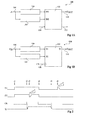
- Figure 1A illustrates a radiation hardened circuit 100 comprising a circuit block 102 having inputs IN1 and IN2.
- the data input IN1 is coupled to and driven by input circuitry 104, which receives an input signal IN on a line 106.
- the input circuitry 104 comprises a plurality of components, for example logic components and/or analog components, that generates the signal at input IN1 as a function of the input signal IN.
- the input circuitry 104 comprises combinational components, such as data buffers or other logic gates and not sequential logic.
- the input circuitry 104 additionally or alternatively comprises one or more analog circuit components such as resistors, capacitors, inductors, transmission lines, etc. In any case, the input circuitry 104 for example does not store data from one clock cycle to the next.
- the data input IN2 is coupled to and driven by input circuitry 104', which is for example an identical duplication of the input circuitry 104, or is at least functionally equivalent to input circuitry 104, and receives the same input signal IN as the input circuitry 104.
- the circuit block 102 for example comprises one or more further inputs 108. Furthermore, the circuit block 102 comprises an output 110 providing an output signal OUT, and for example comprises one or more further outputs 112.
- the circuit block 102 in response to at least one voltage or current change of both of the input signals at inputs IN1 and IN2, the circuit block 102 is for example adapted to apply, immediately or after a time delay, a change of the output signal D OUT .
- the output signal is to at least some extent protected.
- the output signal is determined by the conduction state of at least two transistors (not illustrated in Figure 1 ), one being controlled based on the signal at input IN1, and the other being controlled based on the signal at input 1N2. In this way, at least some changes in the conduction state of only one of the transistors will be countered by the other transistor.
- Figure 1B illustrates the radiation hardened circuit 100 according to a particular example in which the circuit block 102 is a data storage element 102, having data inputs D1 and D2.
- the data storage element 102 is for example a synchronous data storage element, receiving a clock signal CK on input line 108.
- Element 102 provides an output data signal D OUT on output line 110.
- the synchronous data storage element 102 maintains a voltage state on which the output data D OUT is based.
- the data storage element 102 is for example configured such that this logic state can not be altered as a result of radiation hitting any one of its transistors.
- the voltage state stored by the data storage element 102 is also protected from being altered as a result of radiation hitting the input circuitry 104.
- the data storage element 102 is configured such that its stored voltage state is not modified by a change in just one of the data signals D1 and D2.
- Figure 2 is a timing diagram illustrating examples of the input data signals D1 and D2, the clock signal CK, and the output data signal Q of the synchronous data storage element 102 of Figure 1B . It is assumed that all of the data signals D1, D2 and Q for example start low.
- both of the data signals D1 and D2 for example transition to a logic high state at substantially the same time, in response to a change in the input data signal D IN .
- the clock signal CK for example transitions low shortly beforehand, which does not cause any transition on the Q output.
- element 102 At a time t2, a rising edge of the clock signal CK occurs, which triggers shortly afterwards a change in the Q data output of the element 102.
- the data storage element 102 is a D-type latch, the Q data output following the input data when the clock signal is high.
- element 102 could perform any of a wide range of alternative functions.
- element 102 could be a latch that is transparent when the clock is low, a JK flip-flop, an SR flip-flop, or a more complex device.
- the device could also be a D-type flip-flop comprising for example two latches coupled in series, these latches being transparent during opposite phases of the clock signal.
- an ionizing particle for example hits the input circuitry 104', causing a transient of the data signal D2 from a logic high level to a logic low level.
- data signal D1 is unaffected, the voltage state of the data storage element 102, and thus its Q output, is not modified by this transient.
- the data value of the signal D2 for example recovers a short time later to the high state, as determined by the value of the input data D IN .
- the transient results in no permanent modification of the data in the circuit.
- the data signals D1 and D2 both transition to a low state due to a change in the logic state of D IN .
- the clock signal CK for example comprises a falling edge shortly beforehand, which does not cause any transition on the Q output.
- the clock signal CK goes high again, this rising edge for example causing the Q signal to go low a short time later, reflecting the low level of the data signals D1 and D2.
- an ionizing particle for example hits the input circuitry 104, causing a transient of the data signal D1, which goes from the logic low state to a logic high state.
- the data signal D2 does not change state, the voltage state stored by the synchronous element 102 is not altered, and instead the data signal D1 recovers a short time later to the low state, as determined by the value of D IN .
- the data storage element 102 is protected from transients occurring at its data inputs.
- Figure 3 illustrates a radiation hardened circuit 300 according to an alternative embodiment to that of Figure 1B .
- Those features in common with the circuit 100 of Figure 1B are labelled with like reference numerals and will not be described again in detail.
- the circuit 300 comprises a data storage element 302, which is similar to the data storage element 102 of Figure 1B , but comprises, in addition to the data inputs D1 and D2, a pair of clock inputs CK1 and CK2.
- the clock input CK1 is coupled to clock input circuitry 304, which receives an input clock signal CK on an input line 306.
- Circuitry 304 for example comprises one or more clock buffers and/or other logic devices, such as combinational gates and/or sequential elements including clock gating latches.
- the clock input CK2 is coupled to clock input circuitry 304', which also receives the input clock signal CK on line 306.
- Circuitry 304' is for example identical to circuitry 304, or at least functionally equivalent.
- the voltage state of the data storage element 302 is protected from radiation hitting the input circuitry 104 or 104'. Furthermore, the data storage element 302 is additionally protected from radiation hitting the clock input circuitry 304 or 304'.
- the data storage element 302 is for example configured to modify its stored voltage state based on the input data signals D1 and D2 only when both of the signals CK1 and CK2 transition towards the same state, for example to a logic high state.
- only the clock input circuitry 304 in circuit 300 is protected from radiation, and the data input circuitry 104' is omitted, the data storage element 302 comprising a single data input D.
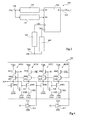
- Figure 4 illustrates the data storage element 302 of Figure 3 in more detail according to an example embodiment.
- Element 302 for example comprises four main branches 402A, 402B, 402C and 402D.
- Branch 402A comprises PMOS transistors 404A and 406A and an NMOS transistor 408A coupled in series between a supply voltage V DD and ground.
- Branch 402B comprises PMOS transistors 404B and 406B and NMOS transistors 408B and 410B coupled between supply voltage V DD and ground.
- Branch 402C comprises PMOS transistors 404C and 406C and an NMOS transistor 408C coupled in series between supply voltage V DD and ground.
- Branch 402D comprises PMOS transistors 404D and 406D and NMOS transistors 408D and 410D coupled in series between supply voltage V DD and ground.
- a node 412 between the transistors 406A and 408A of branch 402A provides the data output signal Q of the data storage element 302.
- Node 412 is also coupled to the gate node of transistor 408B of the branch 402B, to the gate node of transistor 406D of the branch 402D, and to ground via a transistor 413.
- the gates of transistors 413 and 404A receive a reset signal R1.
- a node 414 between the transistors 406B and 408B of the branch 402B receives the data input signal D1 via a switch 415 controlled by the clock signal CK1.
- this switch is implemented by an inverter powered when the clock signal CK1 is low and its inverse CK 1 is high.
- Node 414 is also coupled to the gate of transistor 406A of branch 402A, and of transistor 408C of branch 402C.
- the gates of transistors 404B and 410B are coupled respectively to the clock signals CK 1 and CK1.
- a node 416 between the transistors 406C and 408C of branch 402C is coupled to the gate nodes of transistor 406B of branch 402B and transistor 408D of branch 402D.
- Node 416 is also coupled to ground via a further transistor 418.
- the gate nodes of transistors 404C and 418 receive a second reset signal R2.
- a node 420 between the transistors 406D and 408D of the branch 402D is coupled to the gate of transistor 406C of branch 402C and to the gate of transistor 408A of branch 402A.
- Node 420 also receives the data signal D2 via a switch 421.
- Switch 421 is for example identical to switch 415, except that it is activated by the clock signal CK2 and its inverse CK2 .
- the gate nodes of transistors 404D and 410D are coupled to the clock signals CK2 and CK2 respectively.
- output signal Q of the element 302 is provided by node 412, in alternative embodiments it could be provided by node 416. Furthermore, in some embodiments both of the nodes 412 and 416 could be used to provide identical output data, which could for example be provided to the data inputs of a subsequent pair of combinational logic networks such as blocks 104 and 104' of Figure 3 .
- the data storage element 302 of Figure 4 stores data in the form of high or low voltage states at nodes 412, 414, 416 and 420.
- the voltage states at nodes 412, 414, 416 and 420 are determined by both the signals D1 and D2 when the inverters 415 and 421 are activated.
- transistor 406A is controlled by signal D1 at node 414
- transistor 408A is controlled by the signal D2 at node 420. Therefore, a transient change in one of the signals D1, D2 alone is not sufficient to change the voltage at these nodes.
- a transient at node 414 or 420 caused by a transient of one of the clock signals CK1 or CK2 will not alone cause a change in the voltage state stored at nodes 412, 414, 416 and 420.
- both of the reset signals R1 and R2 are for example at a logic low level. Both of the reset signals R1 and R2 are asserted high to reset the data stored at the storage nodes 412 and 416 to a low level. If only one of the reset signals is asserted however, the reset will not be effective. Thus any transient occurring on only one of the reset lines will not cause a reset of the data storage element 302.
- the data storage element of Figure 4 could be adapted to implement the data storage element 102 of Figure 1B .
- the clock signals CK1 and CK2 can be replaced by the same clock signal CK.
- this data storage element 302 could be adapted to protect the stored states only from transients in the clock path.
- the data signals D1 and D2 could both be replaced by a single data input D applied to each of the switches 415 and 421.
- the reset signals R1 and R2 could be both replaced by a single reset signal applied to each of the transistors 404A, 413, 404C and 418.
- this data storage element 302 could be adapted so that it is controlled by set signals S1 and S2 rather than, or in addition to, the reset signals R1 and R2.
- set signals S1 and S2 rather than, or in addition to, the reset signals R1 and R2.
- a PMOS transistor could be coupled in parallel with transistor 406A and an NMOS transistor could be coupled in series with transistors 408B and 410B, these additional transistors being controlled by a set signal SN1.
- a PMOS transistor could be coupled in parallel with transistor 406C and an NMOS transistor could be coupled in series with transistors 408D and 410D, these additional transistors being controlled by a set signal SN2.
- the data stored at the storage nodes 412 and 416 can be set to a high level when the set signals SN1 and SN2 are low.
- Figure 5 illustrates a phase locked loop circuit 500 according to an example embodiment in which radiation protection can be incorporated based on the techniques described herein above.
- Circuit 500 comprises an input buffer 502, which receives on an input line 504 an input frequency signal CLK IN .
- the buffer 502 also receives a feedback frequency signal CLK FB via a feedback loop.
- Buffer 502 provides the input frequency signal CLK IN and the feedback frequency signal CLK FB to a phase frequency detector (PFD) 506, which compares these signals to generate analog up and down control signals UP and DN.
- the analog control signals UP and DN are provided to a charge pump and loop filter block 508, which generates an analog control voltage V CTRL based on these signals.
- the control voltage V CTRL is in turn provided to a voltage controlled oscillator (VCO) 510.
- VCO voltage controlled oscillator
- a level shifter 512 is for example provided at the output of the VCO 510, and provides a frequency signal CLK OUT on an output line 514.
- the output signal CLK OUT is also provided to the feedback path, which for example comprises a frequency divide-by-two block 516, and a programmable frequency divider 518.
- the divide-by-two block 516 for example reduces the frequency of the clock signal CLK OUT by a factor of two, and provides the resulting signal to the programmable frequency divider 518.
- the programmable frequency divider 518 further divides the signal based on a control signal S, to provide the feedback signal CLK FB provided to buffer 502.
- the frequency of the output signal CLK OUT of the PLL will converge to a value N times that of the input clock frequency CLK IN , where N is equal to overall divisor resulting from the divisions performed by blocks 516 and 518.
- a digital lock detection block 522 and an analog lock detection block 524 provide signals indicating when the output clock signal CLK OUT has settled to a desired frequency and can be relied upon.
- the block 522 provides a coarse lock signal LOCK_C, which is based on a digital processing of the frequency signals CLK IN and CLK FB .
- the block 524 provides a fine lock signal LOCK_F, which is based on an analog and digital processing of the control signals UP and DN generated by the PFD 506.
- circuits of Figures 1A, 1B , 3 and/or 4 are for example incorporated in various parts of the PLL of Figure 4 in order to increase the immunity of this circuit from errors caused by radiation, as will now be described with reference to Figures 6 to 9 .
- FIG. 6 illustrates schematically the phase frequency detector 506 of Figure 5 in more detail.
- the PFD 506 for example comprises a detection stage 602, and an output stage 604.
- the detection stage 602 comprises flip-flops 606A and 606B, each of which is similar to data storage element 302 of Figure 3 .
- the flip-flop 606A receives at both of its clock inputs the frequency signal CLK IN
- the flip-flop 606B receives at its clock inputs the frequency signals CLK FB and CLK FB ' respectively.
- Both of the flip-flops 606A and 606B have their data inputs tied to a logic "1".
- Each of the flip-flops 606A, 606B comprises a pair of duplicated outputs Q1 and Q2, which are coupled to the output stage 604, and also to two redundant two-input AND gates 608A and 608B of stage 602.
- the output Q1 of flip-flop 606A and the output Q2 from the flip-flop 606B are coupled to respective inputs of AND gate 608A
- the output Q2 of flip-flop 606A and the output Q1 from the flip-flop 606B are coupled to respective inputs of AND gate 608B.
- AND gate 608A is coupled to a first reset input R1 of each of the flip-flops 606A, 606B, while the output of AND gate 608B is coupled to a second reset input R2 of each of the flip-flops 606A, 606B.
- each of the flip-flops 606A and 606B are reset when both of the reset signals R1 and R2 are asserted.
- any transient signal induced by radiation hitting either of the AND gates 608A, 608B does not lead to a reset of either of the flip-flops 606A, 606B.
- a transient on only one of the outputs Q1 or Q2 will not cause a reset of the flip-flops 606A, 606B.
- the output stage 604 comprises two redundant buffers 612A and 612A' receiving respectively the Q1 and Q2 data outputs from flip-flop 606A, and two redundant buffers 612B and 612B' respectively receiving the Q1 and Q2 data outputs from flip-flop 606B.
- Buffers 612A and 612A' respectively provide duplicated control signals UP1 and UP2, while buffers 612B and 612B' respectively provide duplicated control signals DN1 and DN2.
- the buffers 612A, 612A', 612B and 612B' may for example further comprise other combinational logic devices (not illustrated in Figure 6 ).
- FIG. 7 illustrates in more detail the feedback path from the charge pump 508 of the PLL through to the programmable frequency divider 518.
- the charge pump block 508 for example receives the duplicated control signals UP1, UP2, DN1 and DN2 generated by the phase frequency detector 506.
- this block for example comprises an analog circuit driven by digital clock signals, such that it is protected from a transient on the signal UP1 or UP2, or on the signal DN1 or DN2.
- all of the data connections linking the various blocks of the feedback path between the VCO 510 and the programmable frequency divider 518 are duplicated.
- the signal CLK IN from the VCO 510 is duplicated and provided to circuits 702 and 702', which are for example identical to each other or at least functionally equivalent.
- the circuits 702 and 702' for example comprise combinational logic such as data buffers and/or other logic gates.
- Each of the circuits 702, 702' provides an output to a corresponding input of the divide-by-two block 516.
- This block for example comprises at least an input latch corresponding to the data storage element 302 described above, in which the data inputs are for example coupled to the inverted data storage outputs, to divide the input frequency by two, and the clock inputs CK1 and CK2 are for example coupled to the outputs of the circuits 702 and 702' respectively, such that any transient caused by radiation hitting the circuit 702 or 702' does not cause errors to be propagated further in the circuit.
- the divide-by-two block 516 for example provides two identical output signals to corresponding circuits 704 and 704' respectively, which again for example comprises combinational logic.
- the circuits 704 and 704' each provide a signal to the programmable frequency divider 518.
- the block 518 for example comprises at least an input latch corresponding to the data storage element 302 described above, such that any transient caused by radiation hitting the circuitry 704 or 704' does not cause errors to be propagated further in the circuit.
- the synchronous data storage elements of block 518 are for example protected from any transient in the circuits 704 or 704', by using the technique described above with reference to the data storage element 302 of Figure 3 .
- the programmable frequency divider 518 provides duplicated output signals CLK FB and CLK' FB , which are each provided to the phase frequency detector 506.
- Figures 8A , 8B and 8D illustrate the charge pump 508 of Figure 7 according to an example embodiment. More generally, the circuits of Figures 8A , 8B and 8D provide examples of an analog implementation of the circuit block 102 of Figure 1 .
- PMOS transistors 802, 804 and NMOS transistors 806, 808, are coupled in series by their main current nodes between nodes 810 and 812.
- Transistors 802 and 804 have their gates coupled to the inverse signals NUP1 and NUP2 of the up control signals UP1 and UP2 respectively, while transistors 806 and 808 have their gates coupled to the down control signals DN1 and DN2 respectively.
- a further two PMOS transistors 814, 816 and NMOS transistors 818, 820 are for example also coupled in series between nodes 810 and 812.
- Transistors 814 and 816 have their gates coupled to the signals UP1 and UP2 respectively, while transistors 818 and 820 have their gates coupled to the inverse signals NDN1 and NDN2 of the down control signals DN1 and DN2 respectively.
- Node 810 is for example coupled to a supply voltage VDD via a PMOS transistor 822 controlled at its gate node by a biasing voltage PBIAS.
- node 812 is for example coupled to ground via an NMOS transistor 824 controlled at its gate node by a biasing voltage NBIAS.
- a node 826 between the PMOS transistor 804 and the NMOS transistor 806 provides an output signal V CTRL , based on which the VCO is controlled.
- a node 828 between the PMOS transistor 816 and the NMOS transistor 818 provides an output signal V CTRL ', which may for example serve as a reference signal. Alternatively, the signal V CTRL ' is not used, the circuitry on the right-hand side in Figure 8B serving only the role of balancing.
- transistors 814 to 820 could be omitted.
- transistors 802 and 804 In operation, when both of the up control signals UP1 and UP2 go high, transistors 802 and 804 will be activated, increasing the voltage at node 826. When both of the down signals DN1 and DN2 go high, transistors 806 and 808 will be activated, decreasing the voltage at node 826. However, when only one of the signals UP1 and UP2, or only one of the signals DN1 and DN2, goes high, for example as a result of radiation, the output voltage VOUT will not be affected.
- transistors 802 and 804 coupled be coupled in parallel between nodes 810 and 826
- transistors 806 and 808 could be coupled in parallel between nodes 826 and 812
- transistors 814 and 816 could be coupled in parallel between nodes 810 and 828
- transistors 818 and 820 could be coupled in parallel between nodes 828 and 812.
- Figure 8B illustrates the charge pump 508 according to an alternative example similar to that of Figure 8A , and in fact includes all of the elements of Figure 8A , which have been labelled in Figure 8B with the same reference numbers. Additionally, the circuit of Figure 8B comprises: PMOS transistors 832 and 834 coupled in series between nodes 810 and 826, in parallel with transistors 802 and 804; NMOS transistors 836 and 838 coupled in series between nodes 826 and 812, in parallel with transistors 806 and 808; PMOS transistors 844 and 846 coupled in series between nodes 810 and 828, in parallel with transistors 814 and 816; and NMOS transistors 848 and 850 coupled in series between nodes 828 and 812, in parallel with transistors 818 and 820.
- PMOS transistors 832 and 834 coupled in series between nodes 810 and 826, in parallel with transistors 802 and 804
- NMOS transistors 836 and 838 coupled in series between nodes 826 and 812, in parallel with
- the transistors 802, 804, 832 and 834 are controlled by signals NUP11, NUP21, NUP12 and NUP22 respectively.
- the transistors 806, 808, 836 and 838 are controlled by signals DN11, DN21, DN12 and DN22 respectively.
- the transistors 814, 816, 844 and 846 are controlled by signals UP11, UP21, UP12 and UP22 respectively.
- the transistors 818, 820, 848 and 850 are controlled by signals NDN11, NDN21, NDN12 and NDN22 respectively.
- Figure 8C illustrates an example of circuitry for generating the various control signals of Figure 8B .
- the input signal UP1 is buffered by a buffer to generate the signal UP11, which is in turn inverted by an inverter to generate the signal NUP11.
- the signal UP1 is also buffered by another buffer to generate signal UP12, which is then inverted by another inverter to generate the signal NUP12.
- the input signal UP2 is buffered by a buffer to generate the signal UP21, which is in turn inverted by an inverter to generate the signal NUP21.
- the signal UP2 is also buffered by another buffer to generate signal UP22, which is then inverted by another inverter to generate the signal NUP22.
- the input signal DN1 is buffered by a buffer to generate the signal DN11, which is in turn inverted by an inverter to generate the signal NDN11.
- the signal DN1 is also buffered by another buffer to generate signal DN12, which is then inverted by another inverter to generate the signal NDN12.
- the input signal DN2 is buffered by a buffer to generate the signal DN21, which is in turn inverted by an inverter to generate the signal NDN21.
- the signal DN2 is also buffered by another buffer to generate signal DN22, which is then inverted by another inverter to generate the signal NDN22.
- Figure 8D illustrates the charge pump 508 according to yet a further embodiment.
- Figure 8B provides an example of a drain switching embodiment
- Figure 8D provides an example of a source switching embodiment.
- This embodiment comprises the same transistors as the embodiment of Figure 8B , controlled by the same controlled signals, which are for example also generated by the circuitry of Figure 8C .
- the transistors in Figure 8D are arranged differently, with the transistor pair 802, 804, and the transistor pair 832, 834, coupled between supply voltage V DD and node 810.
- the transistor pair 806, 808, and the transistor pair 836, 838 are coupled between ground and node 810.
- the transistor pair 814, 816, and the transistor pair 844, 846 are coupled between supply voltage V DD and node 812. Furthermore, the transistor pair 818, 820, and the transistor pair 848, 850, are coupled between ground and node 812. Node 810 is coupled to the output node 826 via PMOS transistor 822, and node 812 is coupled to the output node 826 via NMOS transistor 824.
- Figure 9 illustrates an example of the analog lock detection block 524 according to an example embodiment.
- the block 524 for example comprises duplicated analog portions 902 and 902'.
- the analog portion 902 receives the control signals UP1 and DN1 from the phase frequency detector 506, while the analog portion 902' receives the control signals UP2 and DN2 from the phase frequency detector 506.
- the analog portions 902 and 902' detect, based on the control signals, when the input signals have stabilized, and provides corresponding redundant digital lock control signals CTRL and CTRL' on two output lines 903 and 903' respectively.
- the signal CTRL is provided to a digital portion 904, while the signal CTRL' is provided to a digital portion 904'.
- the digital portions 904 and 904' are for example identical to each other or at least functionally equivalent, and comprise combinational and/or sequential logic.
- These blocks provide respective lock signals LOCK_F and LOCK_F', which are for example provided to a data storage element similar to element 102 or 302 described above, which is outside the PLL.
- Figure 9 demonstrates that analog portions of a circuit may be duplicated in addition to the digital portions in order to protect the analog portions from the effects of radiation.
- An advantage of the embodiments described herein is that a circuit block is protected from radiation hitting input circuitry at one or more of its inputs in a simple and effective manner.
- an output of the circuit block is determined by the conduction state of transistors respectively controlled by duplicated input signals, such that one of the transistors will counter to some extent a change caused by a transient affecting the other transistor.
- the digital data paths, clock paths and low capacitance analog nodes are protected. Protection of the clock paths can be achieved in a simple fashion by clocking a first version of the data signal with a first version of the clock signal, and a second version of the data signal with a second version of the clock signal. Protection of low capacitance analogue parts can be achieved in a simple fashion by duplicating these parts, and providing the duplicated signals to a data storage element as described above.
- the high and low supply voltages are at V DD and ground, it will be apparent that any suitable voltages could be used, which may depend on the transistor technology.
- transistors represented as p-channel MOS transistors could be replaced in alternative embodiments by n-channel MOS transistors, and vice versa.
- the various transistors could be implemented in alternative transistor technologies rather than MOS, such as bipolar.
- phase locked loop circuit has been provided in Figure 5 , it will be apparent to those skilled in the art that there are numerous modifications that could be applied to this circuit.
- the divide-by-two block 516 and/or level shifter 512 could be omitted in some embodiments.
- analog portions 508 and 510 of Figure 7 are not duplicated, in alternative either or both of these portions could be duplicated to provide added protection.
Landscapes
- Physics & Mathematics (AREA)
- Engineering & Computer Science (AREA)
- Computer Hardware Design (AREA)
- Computing Systems (AREA)
- General Engineering & Computer Science (AREA)
- Mathematical Physics (AREA)
- Stabilization Of Oscillater, Synchronisation, Frequency Synthesizers (AREA)
Priority Applications (2)
| Application Number | Priority Date | Filing Date | Title |
|---|---|---|---|
| EP20130305644 EP2804179A1 (de) | 2013-05-17 | 2013-05-17 | Strahlungsgehärtete Schaltung |
| US14/276,567 US20140340133A1 (en) | 2013-05-17 | 2014-05-13 | Radiation hardened circuit |
Applications Claiming Priority (1)
| Application Number | Priority Date | Filing Date | Title |
|---|---|---|---|
| EP20130305644 EP2804179A1 (de) | 2013-05-17 | 2013-05-17 | Strahlungsgehärtete Schaltung |
Publications (1)
| Publication Number | Publication Date |
|---|---|
| EP2804179A1 true EP2804179A1 (de) | 2014-11-19 |
Family
ID=48918328
Family Applications (1)
| Application Number | Title | Priority Date | Filing Date |
|---|---|---|---|
| EP20130305644 Withdrawn EP2804179A1 (de) | 2013-05-17 | 2013-05-17 | Strahlungsgehärtete Schaltung |
Country Status (2)
| Country | Link |
|---|---|
| US (1) | US20140340133A1 (de) |
| EP (1) | EP2804179A1 (de) |
Cited By (1)
| Publication number | Priority date | Publication date | Assignee | Title |
|---|---|---|---|---|
| CN108183706A (zh) * | 2018-01-29 | 2018-06-19 | 中国人民解放军国防科技大学 | 一种抗单粒子翻转的寄存器文件存储阵列写单元 |
Families Citing this family (2)
| Publication number | Priority date | Publication date | Assignee | Title |
|---|---|---|---|---|
| US10848134B2 (en) * | 2015-09-25 | 2020-11-24 | Intel Corporation | Latch with redundancy and circuitry to protect against a soft error |
| US10707879B2 (en) * | 2018-04-13 | 2020-07-07 | KaiKuTek Inc. | Frequency-modulated continuous-wave radar system and frequency tracking method for calibrating frequency gains of a radio frequency signal to approach wideband flatness frequency responses |
Citations (9)
| Publication number | Priority date | Publication date | Assignee | Title |
|---|---|---|---|---|
| US5570313A (en) | 1994-10-18 | 1996-10-29 | Thomson-Csf Semiconducteurs Specifiques | Memory insensitive to disturbances |
| US6421404B1 (en) * | 1998-06-09 | 2002-07-16 | Nec Corporation | Phase-difference detector and clock-recovery circuit using the same |
| US20040257108A1 (en) * | 2003-06-17 | 2004-12-23 | Honeywell International Inc. | Single event hardening of null convention logic circuits |
| US20070205799A1 (en) * | 2006-03-03 | 2007-09-06 | Aeroflex Colorado Springs Inc. | Radiation hardened logic circuit |
| US20090045834A1 (en) * | 2007-08-17 | 2009-02-19 | Raytheon Company | Digital circuits with adaptive resistance to single event upset |
| US20090085627A1 (en) * | 2007-09-28 | 2009-04-02 | Balkaran Gill | Soft error rate hardened latch |
| US20090121765A1 (en) * | 2007-11-08 | 2009-05-14 | Nec Electronics Corporation | Latch circuit and flip-flop circuit |
| US20100253403A1 (en) * | 2009-04-01 | 2010-10-07 | Honeywell International Inc. | Radiation-Hardened Charge Pump Topology |
| US20120139578A1 (en) * | 2010-12-06 | 2012-06-07 | Lavery Kevin P | Soft-error resistant latch |
Family Cites Families (3)
| Publication number | Priority date | Publication date | Assignee | Title |
|---|---|---|---|---|
| KR100445062B1 (ko) * | 2001-11-02 | 2004-08-21 | 주식회사 하이닉스반도체 | 반도체메모리장치의 클럭발생회로 |
| US8754692B2 (en) * | 2008-09-04 | 2014-06-17 | Oracle America, Inc. | Low power and soft error hardened dual edge triggered flip flop |
| US8324951B1 (en) * | 2010-04-08 | 2012-12-04 | Stc.Unm | Dual data rate flip-flop circuit |
-
2013
- 2013-05-17 EP EP20130305644 patent/EP2804179A1/de not_active Withdrawn
-
2014
- 2014-05-13 US US14/276,567 patent/US20140340133A1/en not_active Abandoned
Patent Citations (9)
| Publication number | Priority date | Publication date | Assignee | Title |
|---|---|---|---|---|
| US5570313A (en) | 1994-10-18 | 1996-10-29 | Thomson-Csf Semiconducteurs Specifiques | Memory insensitive to disturbances |
| US6421404B1 (en) * | 1998-06-09 | 2002-07-16 | Nec Corporation | Phase-difference detector and clock-recovery circuit using the same |
| US20040257108A1 (en) * | 2003-06-17 | 2004-12-23 | Honeywell International Inc. | Single event hardening of null convention logic circuits |
| US20070205799A1 (en) * | 2006-03-03 | 2007-09-06 | Aeroflex Colorado Springs Inc. | Radiation hardened logic circuit |
| US20090045834A1 (en) * | 2007-08-17 | 2009-02-19 | Raytheon Company | Digital circuits with adaptive resistance to single event upset |
| US20090085627A1 (en) * | 2007-09-28 | 2009-04-02 | Balkaran Gill | Soft error rate hardened latch |
| US20090121765A1 (en) * | 2007-11-08 | 2009-05-14 | Nec Electronics Corporation | Latch circuit and flip-flop circuit |
| US20100253403A1 (en) * | 2009-04-01 | 2010-10-07 | Honeywell International Inc. | Radiation-Hardened Charge Pump Topology |
| US20120139578A1 (en) * | 2010-12-06 | 2012-06-07 | Lavery Kevin P | Soft-error resistant latch |
Cited By (2)
| Publication number | Priority date | Publication date | Assignee | Title |
|---|---|---|---|---|
| CN108183706A (zh) * | 2018-01-29 | 2018-06-19 | 中国人民解放军国防科技大学 | 一种抗单粒子翻转的寄存器文件存储阵列写单元 |
| CN108183706B (zh) * | 2018-01-29 | 2021-09-07 | 中国人民解放军国防科技大学 | 一种抗单粒子翻转的寄存器文件存储阵列写单元 |
Also Published As
| Publication number | Publication date |
|---|---|
| US20140340133A1 (en) | 2014-11-20 |
Similar Documents
| Publication | Publication Date | Title |
|---|---|---|
| Sidiropoulos et al. | A semidigital dual delay-locked loop | |
| Maneatis | Low-jitter process-independent DLL and PLL based on self-biased techniques | |
| TW538596B (en) | Digitally controlled analog delay locked loop (DLL) | |
| US5426384A (en) | Voltage controlled oscillator (VCO) with symmetrical output and logic gate for use in same | |
| US6667641B1 (en) | Programmable phase shift circuitry | |
| US8416900B2 (en) | Method and circuit for dynamically changing the frequency of clock signals | |
| Lad Kirankumar et al. | A dead-zone-free zero blind-zone high-speed phase frequency detector for charge-pump PLL | |
| US6275555B1 (en) | Digital delay locked loop for adaptive de-skew clock generation | |
| US8451042B2 (en) | Apparatus and system of implementation of digital phase interpolator with improved linearity | |
| US7071751B1 (en) | Counter-controlled delay line | |
| US8633749B2 (en) | Phase-locked loop (PLL) fail-over circuit technique and method to mitigate effects of single-event transients | |
| US6696874B2 (en) | Single-event upset immune flip-flop circuit | |
| US6731147B2 (en) | Method and architecture for self-clocking digital delay locked loop | |
| US6834093B1 (en) | Frequency comparator circuit | |
| GB2413020A (en) | High speed CMOS flip-flops and clocked logic gates | |
| US6710637B1 (en) | Non-overlap clock circuit | |
| EP2804179A1 (de) | Strahlungsgehärtete Schaltung | |
| US9647671B2 (en) | High performance phase frequency detectors | |
| CN111819795B (zh) | 抗辐射的d触发器电路 | |
| Jia | A delay-locked loop for multiple clock phases/delays generation | |
| Zhang et al. | A see insensitive cml voltage controlled oscillator in 65nm cmos | |
| Dhoble et al. | A review paper on design of positive edge triggered D flip-flop using VLSI technology | |
| US11075639B1 (en) | Frequency divider with delay compensation | |
| US5920207A (en) | Asynchronous phase detector having a variable dead zone | |
| CN1726643A (zh) | 使用时间周期抑制器的低锁定时间的延迟锁定环 |
Legal Events
| Date | Code | Title | Description |
|---|---|---|---|
| PUAI | Public reference made under article 153(3) epc to a published international application that has entered the european phase |
Free format text: ORIGINAL CODE: 0009012 |
|
| 17P | Request for examination filed |
Effective date: 20130517 |
|
| AK | Designated contracting states |
Kind code of ref document: A1 Designated state(s): AL AT BE BG CH CY CZ DE DK EE ES FI FR GB GR HR HU IE IS IT LI LT LU LV MC MK MT NL NO PL PT RO RS SE SI SK SM TR |
|
| AX | Request for extension of the european patent |
Extension state: BA ME |
|
| R17P | Request for examination filed (corrected) |
Effective date: 20150512 |
|
| RBV | Designated contracting states (corrected) |
Designated state(s): AL AT BE BG CH CY CZ DE DK EE ES FI FR GB GR HR HU IE IS IT LI LT LU LV MC MK MT NL NO PL PT RO RS SE SI SK SM TR |
|
| 17Q | First examination report despatched |
Effective date: 20200102 |
|
| STAA | Information on the status of an ep patent application or granted ep patent |
Free format text: STATUS: THE APPLICATION IS DEEMED TO BE WITHDRAWN |
|
| 18D | Application deemed to be withdrawn |
Effective date: 20200603 |