EP2804209A1 - Module électronique moulé - Google Patents
Module électronique moulé Download PDFInfo
- Publication number
- EP2804209A1 EP2804209A1 EP13168251.0A EP13168251A EP2804209A1 EP 2804209 A1 EP2804209 A1 EP 2804209A1 EP 13168251 A EP13168251 A EP 13168251A EP 2804209 A1 EP2804209 A1 EP 2804209A1
- Authority
- EP
- European Patent Office
- Prior art keywords
- substrate
- semiconductor device
- bonding
- moulding
- moulding material
- Prior art date
- Legal status (The legal status is an assumption and is not a legal conclusion. Google has not performed a legal analysis and makes no representation as to the accuracy of the status listed.)
- Withdrawn
Links
Images

Classifications
-
- H—ELECTRICITY
- H10—SEMICONDUCTOR DEVICES; ELECTRIC SOLID-STATE DEVICES NOT OTHERWISE PROVIDED FOR
- H10W—GENERIC PACKAGES, INTERCONNECTIONS, CONNECTORS OR OTHER CONSTRUCTIONAL DETAILS OF DEVICES COVERED BY CLASS H10
- H10W70/00—Package substrates; Interposers; Redistribution layers [RDL]
- H10W70/40—Leadframes
- H10W70/464—Additional interconnections in combination with leadframes
- H10W70/466—Tape carriers or flat leads
-
- H—ELECTRICITY
- H10—SEMICONDUCTOR DEVICES; ELECTRIC SOLID-STATE DEVICES NOT OTHERWISE PROVIDED FOR
- H10W—GENERIC PACKAGES, INTERCONNECTIONS, CONNECTORS OR OTHER CONSTRUCTIONAL DETAILS OF DEVICES COVERED BY CLASS H10
- H10W74/00—Encapsulations, e.g. protective coatings
- H10W74/01—Manufacture or treatment
- H10W74/016—Manufacture or treatment using moulds
- H10W74/017—Auxiliary layers for moulds, e.g. release layers or layers preventing residue
-
- H—ELECTRICITY
- H10—SEMICONDUCTOR DEVICES; ELECTRIC SOLID-STATE DEVICES NOT OTHERWISE PROVIDED FOR
- H10W—GENERIC PACKAGES, INTERCONNECTIONS, CONNECTORS OR OTHER CONSTRUCTIONAL DETAILS OF DEVICES COVERED BY CLASS H10
- H10W90/00—Package configurations
-
- H—ELECTRICITY
- H10—SEMICONDUCTOR DEVICES; ELECTRIC SOLID-STATE DEVICES NOT OTHERWISE PROVIDED FOR
- H10W—GENERIC PACKAGES, INTERCONNECTIONS, CONNECTORS OR OTHER CONSTRUCTIONAL DETAILS OF DEVICES COVERED BY CLASS H10
- H10W72/00—Interconnections or connectors in packages
- H10W72/01—Manufacture or treatment
- H10W72/013—Manufacture or treatment of die-attach connectors
- H10W72/01308—Manufacture or treatment of die-attach connectors using permanent auxiliary members, e.g. using alignment marks
-
- H—ELECTRICITY
- H10—SEMICONDUCTOR DEVICES; ELECTRIC SOLID-STATE DEVICES NOT OTHERWISE PROVIDED FOR
- H10W—GENERIC PACKAGES, INTERCONNECTIONS, CONNECTORS OR OTHER CONSTRUCTIONAL DETAILS OF DEVICES COVERED BY CLASS H10
- H10W72/00—Interconnections or connectors in packages
- H10W72/01—Manufacture or treatment
- H10W72/013—Manufacture or treatment of die-attach connectors
- H10W72/01321—Manufacture or treatment of die-attach connectors using local deposition
- H10W72/01323—Manufacture or treatment of die-attach connectors using local deposition in liquid form, e.g. by dispensing droplets or by screen printing
-
- H—ELECTRICITY
- H10—SEMICONDUCTOR DEVICES; ELECTRIC SOLID-STATE DEVICES NOT OTHERWISE PROVIDED FOR
- H10W—GENERIC PACKAGES, INTERCONNECTIONS, CONNECTORS OR OTHER CONSTRUCTIONAL DETAILS OF DEVICES COVERED BY CLASS H10
- H10W72/00—Interconnections or connectors in packages
- H10W72/071—Connecting or disconnecting
- H10W72/073—Connecting or disconnecting of die-attach connectors
-
- H—ELECTRICITY
- H10—SEMICONDUCTOR DEVICES; ELECTRIC SOLID-STATE DEVICES NOT OTHERWISE PROVIDED FOR
- H10W—GENERIC PACKAGES, INTERCONNECTIONS, CONNECTORS OR OTHER CONSTRUCTIONAL DETAILS OF DEVICES COVERED BY CLASS H10
- H10W72/00—Interconnections or connectors in packages
- H10W72/071—Connecting or disconnecting
- H10W72/073—Connecting or disconnecting of die-attach connectors
- H10W72/07331—Connecting techniques
-
- H—ELECTRICITY
- H10—SEMICONDUCTOR DEVICES; ELECTRIC SOLID-STATE DEVICES NOT OTHERWISE PROVIDED FOR
- H10W—GENERIC PACKAGES, INTERCONNECTIONS, CONNECTORS OR OTHER CONSTRUCTIONAL DETAILS OF DEVICES COVERED BY CLASS H10
- H10W72/00—Interconnections or connectors in packages
- H10W72/071—Connecting or disconnecting
- H10W72/073—Connecting or disconnecting of die-attach connectors
- H10W72/07331—Connecting techniques
- H10W72/07336—Soldering or alloying
-
- H—ELECTRICITY
- H10—SEMICONDUCTOR DEVICES; ELECTRIC SOLID-STATE DEVICES NOT OTHERWISE PROVIDED FOR
- H10W—GENERIC PACKAGES, INTERCONNECTIONS, CONNECTORS OR OTHER CONSTRUCTIONAL DETAILS OF DEVICES COVERED BY CLASS H10
- H10W72/00—Interconnections or connectors in packages
- H10W72/071—Connecting or disconnecting
- H10W72/073—Connecting or disconnecting of die-attach connectors
- H10W72/07351—Connecting or disconnecting of die-attach connectors characterised by changes in properties of the die-attach connectors during connecting
- H10W72/07354—Connecting or disconnecting of die-attach connectors characterised by changes in properties of the die-attach connectors during connecting changes in dispositions
-
- H—ELECTRICITY
- H10—SEMICONDUCTOR DEVICES; ELECTRIC SOLID-STATE DEVICES NOT OTHERWISE PROVIDED FOR
- H10W—GENERIC PACKAGES, INTERCONNECTIONS, CONNECTORS OR OTHER CONSTRUCTIONAL DETAILS OF DEVICES COVERED BY CLASS H10
- H10W72/00—Interconnections or connectors in packages
- H10W72/071—Connecting or disconnecting
- H10W72/075—Connecting or disconnecting of bond wires
-
- H—ELECTRICITY
- H10—SEMICONDUCTOR DEVICES; ELECTRIC SOLID-STATE DEVICES NOT OTHERWISE PROVIDED FOR
- H10W—GENERIC PACKAGES, INTERCONNECTIONS, CONNECTORS OR OTHER CONSTRUCTIONAL DETAILS OF DEVICES COVERED BY CLASS H10
- H10W72/00—Interconnections or connectors in packages
- H10W72/071—Connecting or disconnecting
- H10W72/075—Connecting or disconnecting of bond wires
- H10W72/07531—Techniques
- H10W72/07532—Compression bonding, e.g. thermocompression bonding
- H10W72/07533—Ultrasonic bonding, e.g. thermosonic bonding
-
- H—ELECTRICITY
- H10—SEMICONDUCTOR DEVICES; ELECTRIC SOLID-STATE DEVICES NOT OTHERWISE PROVIDED FOR
- H10W—GENERIC PACKAGES, INTERCONNECTIONS, CONNECTORS OR OTHER CONSTRUCTIONAL DETAILS OF DEVICES COVERED BY CLASS H10
- H10W72/00—Interconnections or connectors in packages
- H10W72/071—Connecting or disconnecting
- H10W72/076—Connecting or disconnecting of strap connectors
- H10W72/07631—Techniques
-
- H—ELECTRICITY
- H10—SEMICONDUCTOR DEVICES; ELECTRIC SOLID-STATE DEVICES NOT OTHERWISE PROVIDED FOR
- H10W—GENERIC PACKAGES, INTERCONNECTIONS, CONNECTORS OR OTHER CONSTRUCTIONAL DETAILS OF DEVICES COVERED BY CLASS H10
- H10W72/00—Interconnections or connectors in packages
- H10W72/071—Connecting or disconnecting
- H10W72/076—Connecting or disconnecting of strap connectors
- H10W72/07631—Techniques
- H10W72/07636—Soldering or alloying
-
- H—ELECTRICITY
- H10—SEMICONDUCTOR DEVICES; ELECTRIC SOLID-STATE DEVICES NOT OTHERWISE PROVIDED FOR
- H10W—GENERIC PACKAGES, INTERCONNECTIONS, CONNECTORS OR OTHER CONSTRUCTIONAL DETAILS OF DEVICES COVERED BY CLASS H10
- H10W72/00—Interconnections or connectors in packages
- H10W72/071—Connecting or disconnecting
- H10W72/076—Connecting or disconnecting of strap connectors
- H10W72/07631—Techniques
- H10W72/07637—Techniques using a polymer adhesive, e.g. an adhesive based on silicone or epoxy
-
- H—ELECTRICITY
- H10—SEMICONDUCTOR DEVICES; ELECTRIC SOLID-STATE DEVICES NOT OTHERWISE PROVIDED FOR
- H10W—GENERIC PACKAGES, INTERCONNECTIONS, CONNECTORS OR OTHER CONSTRUCTIONAL DETAILS OF DEVICES COVERED BY CLASS H10
- H10W72/00—Interconnections or connectors in packages
- H10W72/30—Die-attach connectors
- H10W72/341—Dispositions of die-attach connectors, e.g. layouts
- H10W72/347—Dispositions of multiple die-attach connectors
-
- H—ELECTRICITY
- H10—SEMICONDUCTOR DEVICES; ELECTRIC SOLID-STATE DEVICES NOT OTHERWISE PROVIDED FOR
- H10W—GENERIC PACKAGES, INTERCONNECTIONS, CONNECTORS OR OTHER CONSTRUCTIONAL DETAILS OF DEVICES COVERED BY CLASS H10
- H10W72/00—Interconnections or connectors in packages
- H10W72/30—Die-attach connectors
- H10W72/351—Materials of die-attach connectors
- H10W72/352—Materials of die-attach connectors comprising metals or metalloids, e.g. solders
-
- H—ELECTRICITY
- H10—SEMICONDUCTOR DEVICES; ELECTRIC SOLID-STATE DEVICES NOT OTHERWISE PROVIDED FOR
- H10W—GENERIC PACKAGES, INTERCONNECTIONS, CONNECTORS OR OTHER CONSTRUCTIONAL DETAILS OF DEVICES COVERED BY CLASS H10
- H10W72/00—Interconnections or connectors in packages
- H10W72/30—Die-attach connectors
- H10W72/351—Materials of die-attach connectors
- H10W72/353—Materials of die-attach connectors not comprising solid metals or solid metalloids, e.g. ceramics
-
- H—ELECTRICITY
- H10—SEMICONDUCTOR DEVICES; ELECTRIC SOLID-STATE DEVICES NOT OTHERWISE PROVIDED FOR
- H10W—GENERIC PACKAGES, INTERCONNECTIONS, CONNECTORS OR OTHER CONSTRUCTIONAL DETAILS OF DEVICES COVERED BY CLASS H10
- H10W72/00—Interconnections or connectors in packages
- H10W72/30—Die-attach connectors
- H10W72/351—Materials of die-attach connectors
- H10W72/353—Materials of die-attach connectors not comprising solid metals or solid metalloids, e.g. ceramics
- H10W72/354—Materials of die-attach connectors not comprising solid metals or solid metalloids, e.g. ceramics comprising polymers
-
- H—ELECTRICITY
- H10—SEMICONDUCTOR DEVICES; ELECTRIC SOLID-STATE DEVICES NOT OTHERWISE PROVIDED FOR
- H10W—GENERIC PACKAGES, INTERCONNECTIONS, CONNECTORS OR OTHER CONSTRUCTIONAL DETAILS OF DEVICES COVERED BY CLASS H10
- H10W72/00—Interconnections or connectors in packages
- H10W72/50—Bond wires
- H10W72/541—Dispositions of bond wires
- H10W72/547—Dispositions of multiple bond wires
- H10W72/5473—Dispositions of multiple bond wires multiple bond wires connected to a common bond pad
-
- H—ELECTRICITY
- H10—SEMICONDUCTOR DEVICES; ELECTRIC SOLID-STATE DEVICES NOT OTHERWISE PROVIDED FOR
- H10W—GENERIC PACKAGES, INTERCONNECTIONS, CONNECTORS OR OTHER CONSTRUCTIONAL DETAILS OF DEVICES COVERED BY CLASS H10
- H10W72/00—Interconnections or connectors in packages
- H10W72/50—Bond wires
- H10W72/59—Bond pads specially adapted therefor
-
- H—ELECTRICITY
- H10—SEMICONDUCTOR DEVICES; ELECTRIC SOLID-STATE DEVICES NOT OTHERWISE PROVIDED FOR
- H10W—GENERIC PACKAGES, INTERCONNECTIONS, CONNECTORS OR OTHER CONSTRUCTIONAL DETAILS OF DEVICES COVERED BY CLASS H10
- H10W72/00—Interconnections or connectors in packages
- H10W72/60—Strap connectors, e.g. thick copper clips for grounding of power devices
- H10W72/651—Materials of strap connectors
- H10W72/652—Materials of strap connectors comprising metals or metalloids, e.g. silver
-
- H—ELECTRICITY
- H10—SEMICONDUCTOR DEVICES; ELECTRIC SOLID-STATE DEVICES NOT OTHERWISE PROVIDED FOR
- H10W—GENERIC PACKAGES, INTERCONNECTIONS, CONNECTORS OR OTHER CONSTRUCTIONAL DETAILS OF DEVICES COVERED BY CLASS H10
- H10W72/00—Interconnections or connectors in packages
- H10W72/851—Dispositions of multiple connectors or interconnections
- H10W72/853—On the same surface
- H10W72/865—Die-attach connectors and bond wires
-
- H—ELECTRICITY
- H10—SEMICONDUCTOR DEVICES; ELECTRIC SOLID-STATE DEVICES NOT OTHERWISE PROVIDED FOR
- H10W—GENERIC PACKAGES, INTERCONNECTIONS, CONNECTORS OR OTHER CONSTRUCTIONAL DETAILS OF DEVICES COVERED BY CLASS H10
- H10W72/00—Interconnections or connectors in packages
- H10W72/851—Dispositions of multiple connectors or interconnections
- H10W72/853—On the same surface
- H10W72/871—Bond wires and strap connectors
-
- H—ELECTRICITY
- H10—SEMICONDUCTOR DEVICES; ELECTRIC SOLID-STATE DEVICES NOT OTHERWISE PROVIDED FOR
- H10W—GENERIC PACKAGES, INTERCONNECTIONS, CONNECTORS OR OTHER CONSTRUCTIONAL DETAILS OF DEVICES COVERED BY CLASS H10
- H10W72/00—Interconnections or connectors in packages
- H10W72/851—Dispositions of multiple connectors or interconnections
- H10W72/874—On different surfaces
- H10W72/884—Die-attach connectors and bond wires
-
- H—ELECTRICITY
- H10—SEMICONDUCTOR DEVICES; ELECTRIC SOLID-STATE DEVICES NOT OTHERWISE PROVIDED FOR
- H10W—GENERIC PACKAGES, INTERCONNECTIONS, CONNECTORS OR OTHER CONSTRUCTIONAL DETAILS OF DEVICES COVERED BY CLASS H10
- H10W72/00—Interconnections or connectors in packages
- H10W72/851—Dispositions of multiple connectors or interconnections
- H10W72/874—On different surfaces
- H10W72/886—Die-attach connectors and strap connectors
-
- H—ELECTRICITY
- H10—SEMICONDUCTOR DEVICES; ELECTRIC SOLID-STATE DEVICES NOT OTHERWISE PROVIDED FOR
- H10W—GENERIC PACKAGES, INTERCONNECTIONS, CONNECTORS OR OTHER CONSTRUCTIONAL DETAILS OF DEVICES COVERED BY CLASS H10
- H10W72/00—Interconnections or connectors in packages
- H10W72/90—Bond pads, in general
- H10W72/921—Structures or relative sizes of bond pads
- H10W72/926—Multiple bond pads having different sizes
-
- H—ELECTRICITY
- H10—SEMICONDUCTOR DEVICES; ELECTRIC SOLID-STATE DEVICES NOT OTHERWISE PROVIDED FOR
- H10W—GENERIC PACKAGES, INTERCONNECTIONS, CONNECTORS OR OTHER CONSTRUCTIONAL DETAILS OF DEVICES COVERED BY CLASS H10
- H10W72/00—Interconnections or connectors in packages
- H10W72/90—Bond pads, in general
- H10W72/941—Dispositions of bond pads
- H10W72/944—Dispositions of multiple bond pads
-
- H—ELECTRICITY
- H10—SEMICONDUCTOR DEVICES; ELECTRIC SOLID-STATE DEVICES NOT OTHERWISE PROVIDED FOR
- H10W—GENERIC PACKAGES, INTERCONNECTIONS, CONNECTORS OR OTHER CONSTRUCTIONAL DETAILS OF DEVICES COVERED BY CLASS H10
- H10W74/00—Encapsulations, e.g. protective coatings
-
- H—ELECTRICITY
- H10—SEMICONDUCTOR DEVICES; ELECTRIC SOLID-STATE DEVICES NOT OTHERWISE PROVIDED FOR
- H10W—GENERIC PACKAGES, INTERCONNECTIONS, CONNECTORS OR OTHER CONSTRUCTIONAL DETAILS OF DEVICES COVERED BY CLASS H10
- H10W74/00—Encapsulations, e.g. protective coatings
- H10W74/10—Encapsulations, e.g. protective coatings characterised by their shape or disposition
-
- H—ELECTRICITY
- H10—SEMICONDUCTOR DEVICES; ELECTRIC SOLID-STATE DEVICES NOT OTHERWISE PROVIDED FOR
- H10W—GENERIC PACKAGES, INTERCONNECTIONS, CONNECTORS OR OTHER CONSTRUCTIONAL DETAILS OF DEVICES COVERED BY CLASS H10
- H10W74/00—Encapsulations, e.g. protective coatings
- H10W74/10—Encapsulations, e.g. protective coatings characterised by their shape or disposition
- H10W74/111—Encapsulations, e.g. protective coatings characterised by their shape or disposition the semiconductor body being completely enclosed
- H10W74/114—Encapsulations, e.g. protective coatings characterised by their shape or disposition the semiconductor body being completely enclosed by a substrate and the encapsulations
-
- H—ELECTRICITY
- H10—SEMICONDUCTOR DEVICES; ELECTRIC SOLID-STATE DEVICES NOT OTHERWISE PROVIDED FOR
- H10W—GENERIC PACKAGES, INTERCONNECTIONS, CONNECTORS OR OTHER CONSTRUCTIONAL DETAILS OF DEVICES COVERED BY CLASS H10
- H10W90/00—Package configurations
- H10W90/401—Package configurations characterised by multiple insulating or insulated package substrates, interposers or RDLs
-
- H—ELECTRICITY
- H10—SEMICONDUCTOR DEVICES; ELECTRIC SOLID-STATE DEVICES NOT OTHERWISE PROVIDED FOR
- H10W—GENERIC PACKAGES, INTERCONNECTIONS, CONNECTORS OR OTHER CONSTRUCTIONAL DETAILS OF DEVICES COVERED BY CLASS H10
- H10W90/00—Package configurations
- H10W90/701—Package configurations characterised by the relative positions of pads or connectors relative to package parts
- H10W90/731—Package configurations characterised by the relative positions of pads or connectors relative to package parts of die-attach connectors
- H10W90/734—Package configurations characterised by the relative positions of pads or connectors relative to package parts of die-attach connectors between a chip and a stacked insulating package substrate, interposer or RDL
-
- H—ELECTRICITY
- H10—SEMICONDUCTOR DEVICES; ELECTRIC SOLID-STATE DEVICES NOT OTHERWISE PROVIDED FOR
- H10W—GENERIC PACKAGES, INTERCONNECTIONS, CONNECTORS OR OTHER CONSTRUCTIONAL DETAILS OF DEVICES COVERED BY CLASS H10
- H10W90/00—Package configurations
- H10W90/701—Package configurations characterised by the relative positions of pads or connectors relative to package parts
- H10W90/731—Package configurations characterised by the relative positions of pads or connectors relative to package parts of die-attach connectors
- H10W90/736—Package configurations characterised by the relative positions of pads or connectors relative to package parts of die-attach connectors between a chip and a stacked lead frame, conducting package substrate or heat sink
-
- H—ELECTRICITY
- H10—SEMICONDUCTOR DEVICES; ELECTRIC SOLID-STATE DEVICES NOT OTHERWISE PROVIDED FOR
- H10W—GENERIC PACKAGES, INTERCONNECTIONS, CONNECTORS OR OTHER CONSTRUCTIONAL DETAILS OF DEVICES COVERED BY CLASS H10
- H10W90/00—Package configurations
- H10W90/701—Package configurations characterised by the relative positions of pads or connectors relative to package parts
- H10W90/751—Package configurations characterised by the relative positions of pads or connectors relative to package parts of bond wires
- H10W90/754—Package configurations characterised by the relative positions of pads or connectors relative to package parts of bond wires between a chip and a stacked insulating package substrate, interposer or RDL
-
- H—ELECTRICITY
- H10—SEMICONDUCTOR DEVICES; ELECTRIC SOLID-STATE DEVICES NOT OTHERWISE PROVIDED FOR
- H10W—GENERIC PACKAGES, INTERCONNECTIONS, CONNECTORS OR OTHER CONSTRUCTIONAL DETAILS OF DEVICES COVERED BY CLASS H10
- H10W90/00—Package configurations
- H10W90/701—Package configurations characterised by the relative positions of pads or connectors relative to package parts
- H10W90/761—Package configurations characterised by the relative positions of pads or connectors relative to package parts of strap connectors
- H10W90/763—Package configurations characterised by the relative positions of pads or connectors relative to package parts of strap connectors between laterally-adjacent chips
-
- H—ELECTRICITY
- H10—SEMICONDUCTOR DEVICES; ELECTRIC SOLID-STATE DEVICES NOT OTHERWISE PROVIDED FOR
- H10W—GENERIC PACKAGES, INTERCONNECTIONS, CONNECTORS OR OTHER CONSTRUCTIONAL DETAILS OF DEVICES COVERED BY CLASS H10
- H10W90/00—Package configurations
- H10W90/701—Package configurations characterised by the relative positions of pads or connectors relative to package parts
- H10W90/761—Package configurations characterised by the relative positions of pads or connectors relative to package parts of strap connectors
- H10W90/764—Package configurations characterised by the relative positions of pads or connectors relative to package parts of strap connectors between a chip and a stacked insulating package substrate, interposer or RDL
-
- H—ELECTRICITY
- H10—SEMICONDUCTOR DEVICES; ELECTRIC SOLID-STATE DEVICES NOT OTHERWISE PROVIDED FOR
- H10W—GENERIC PACKAGES, INTERCONNECTIONS, CONNECTORS OR OTHER CONSTRUCTIONAL DETAILS OF DEVICES COVERED BY CLASS H10
- H10W90/00—Package configurations
- H10W90/701—Package configurations characterised by the relative positions of pads or connectors relative to package parts
- H10W90/761—Package configurations characterised by the relative positions of pads or connectors relative to package parts of strap connectors
- H10W90/766—Package configurations characterised by the relative positions of pads or connectors relative to package parts of strap connectors between a chip and a stacked lead frame, conducting package substrate or heat sink
Definitions
- Ag sintering may provide a robust and reliable connection.
- a planar structure is used for applying the necessary sintering pressures without deforming the side of the semiconductor device carrying the bonding area, for example the top emitter contact.
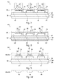
- the combination with a moulding step, which results in an opening above the bonding area, may facilitates the sintering step.
- the first and/or second substrate is a lead frame, PCB, flex print or metallized ceramic.
- the first substrate may be a lead frame or a PCB and the second substrate may be a metallised ceramic.
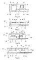
- the method further comprises the step of: structuring the second substrate such that the second substrate has a protrusion fitting into the opening in the moulding material.
- the protrusion may conform to the opening, for example may have bevelled edges, too.
- the second substrate may be pressed and/or etched.
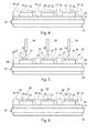
- a post-cure process may be performed for a final cross linking of the moulding material 32, which may be an epoxy matrix.
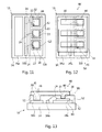
- a second substrate 46 is bonded to the bonding areas of the semiconductor devices 12 through the opening 34.
- the second substrate 46 may be an emitter contact which is sintered with a sintering paste or adhesive or soldered to the bonding area 20 on the semiconductor 12.
Landscapes
- Cooling Or The Like Of Semiconductors Or Solid State Devices (AREA)
Priority Applications (1)
| Application Number | Priority Date | Filing Date | Title |
|---|---|---|---|
| EP13168251.0A EP2804209A1 (fr) | 2013-05-17 | 2013-05-17 | Module électronique moulé |
Applications Claiming Priority (1)
| Application Number | Priority Date | Filing Date | Title |
|---|---|---|---|
| EP13168251.0A EP2804209A1 (fr) | 2013-05-17 | 2013-05-17 | Module électronique moulé |
Publications (1)
| Publication Number | Publication Date |
|---|---|
| EP2804209A1 true EP2804209A1 (fr) | 2014-11-19 |
Family
ID=48482925
Family Applications (1)
| Application Number | Title | Priority Date | Filing Date |
|---|---|---|---|
| EP13168251.0A Withdrawn EP2804209A1 (fr) | 2013-05-17 | 2013-05-17 | Module électronique moulé |
Country Status (1)
| Country | Link |
|---|---|
| EP (1) | EP2804209A1 (fr) |
Cited By (7)
| Publication number | Priority date | Publication date | Assignee | Title |
|---|---|---|---|---|
| EP3059761A3 (fr) * | 2015-02-17 | 2016-11-02 | SFI Electronics Technology Inc. | Composant à montage en surface avec une ou plusieurs puces entre deux cartes de circuit imprimé et procédé de production de celui-ci |
| DE102015108700A1 (de) * | 2015-06-02 | 2016-12-08 | Infineon Technologies Austria Ag | Halbleiter-Leistungs-Package und Verfahren zu ihrer Herstellung |
| WO2017016808A1 (fr) * | 2015-07-30 | 2017-02-02 | Danfoss Silicon Power Gmbh | Module semi-conducteur de puissance |
| DE102015118664A1 (de) * | 2015-10-30 | 2017-05-04 | Infineon Technologies Ag | Verfahren zur herstellung eines leistungshalbleitermoduls |
| EP3584833A1 (fr) * | 2018-06-19 | 2019-12-25 | Mitsubishi Electric R&D Centre Europe B.V. | Ensemble d'alimentation électrique et module de puissance à alignement amélioré |
| CN113519043A (zh) * | 2019-03-04 | 2021-10-19 | 丹佛斯硅动力有限责任公司 | 用于通过压力辅助低温烧结工艺来制造电子部件的压力烧结装置和方法 |
| EP4227995A1 (fr) * | 2022-02-09 | 2023-08-16 | Hitachi Energy Switzerland AG | Module d'électronique de puissance et son procédé de fabrication |
Citations (8)
| Publication number | Priority date | Publication date | Assignee | Title |
|---|---|---|---|---|
| DE3637513A1 (de) * | 1986-11-04 | 1988-05-11 | Semikron Elektronik Gmbh | Verfahren zum herstellen feinstrukturierter kontaktelektroden von leistungs-halbleiterbauelementen |
| DE19617055C1 (de) * | 1996-04-29 | 1997-06-26 | Semikron Elektronik Gmbh | Halbleiterleistungsmodul hoher Packungsdichte in Mehrschichtbauweise |
| WO2003030247A2 (fr) * | 2001-09-28 | 2003-04-10 | Siemens Aktiengesellschaft | Procede d'etablissement de contact pour des surfaces de contact electriques situees sur un substrat et dispositif constitue d'un substrat pourvu de surfaces de contact electriques |
| US20030132530A1 (en) * | 1999-11-24 | 2003-07-17 | Takanori Teshima | Semiconductor device having radiation structure and method for manufacturing semiconductor device having radiation structure |
| DE102004061936A1 (de) * | 2004-12-22 | 2006-07-06 | Siemens Ag | Anordnung eines Halbleitermoduls und einer elektrischen Verschienung |
| DE102007041926A1 (de) * | 2007-09-04 | 2009-03-05 | Siemens Ag | Verfahren zur elektrischen Isolierung beziehungsweise elektrischen Kontaktierung von ungehäusten elektronischen Bauelementen bei strukturierter Verkapselung |
| WO2012043149A1 (fr) * | 2010-09-30 | 2012-04-05 | 日立オートモティブシステムズ株式会社 | Module semi-conducteur de puissance et son procédé de fabrication |
| US20130235636A1 (en) * | 2010-11-29 | 2013-09-12 | Toyota Jidosha Kabushiki Kaisha | Power module |
-
2013
- 2013-05-17 EP EP13168251.0A patent/EP2804209A1/fr not_active Withdrawn
Patent Citations (8)
| Publication number | Priority date | Publication date | Assignee | Title |
|---|---|---|---|---|
| DE3637513A1 (de) * | 1986-11-04 | 1988-05-11 | Semikron Elektronik Gmbh | Verfahren zum herstellen feinstrukturierter kontaktelektroden von leistungs-halbleiterbauelementen |
| DE19617055C1 (de) * | 1996-04-29 | 1997-06-26 | Semikron Elektronik Gmbh | Halbleiterleistungsmodul hoher Packungsdichte in Mehrschichtbauweise |
| US20030132530A1 (en) * | 1999-11-24 | 2003-07-17 | Takanori Teshima | Semiconductor device having radiation structure and method for manufacturing semiconductor device having radiation structure |
| WO2003030247A2 (fr) * | 2001-09-28 | 2003-04-10 | Siemens Aktiengesellschaft | Procede d'etablissement de contact pour des surfaces de contact electriques situees sur un substrat et dispositif constitue d'un substrat pourvu de surfaces de contact electriques |
| DE102004061936A1 (de) * | 2004-12-22 | 2006-07-06 | Siemens Ag | Anordnung eines Halbleitermoduls und einer elektrischen Verschienung |
| DE102007041926A1 (de) * | 2007-09-04 | 2009-03-05 | Siemens Ag | Verfahren zur elektrischen Isolierung beziehungsweise elektrischen Kontaktierung von ungehäusten elektronischen Bauelementen bei strukturierter Verkapselung |
| WO2012043149A1 (fr) * | 2010-09-30 | 2012-04-05 | 日立オートモティブシステムズ株式会社 | Module semi-conducteur de puissance et son procédé de fabrication |
| US20130235636A1 (en) * | 2010-11-29 | 2013-09-12 | Toyota Jidosha Kabushiki Kaisha | Power module |
Cited By (19)
| Publication number | Priority date | Publication date | Assignee | Title |
|---|---|---|---|---|
| EP3059761A3 (fr) * | 2015-02-17 | 2016-11-02 | SFI Electronics Technology Inc. | Composant à montage en surface avec une ou plusieurs puces entre deux cartes de circuit imprimé et procédé de production de celui-ci |
| US10256119B2 (en) | 2015-06-02 | 2019-04-09 | Infineon Technologies Austria Ag | Method of manufacturing a semiconductor power package |
| DE102015108700A1 (de) * | 2015-06-02 | 2016-12-08 | Infineon Technologies Austria Ag | Halbleiter-Leistungs-Package und Verfahren zu ihrer Herstellung |
| DE102015108700B4 (de) | 2015-06-02 | 2025-01-09 | Infineon Technologies Austria Ag | Halbleiter-Leistungs-Package und Verfahren zu ihrer Herstellung |
| US10734250B2 (en) | 2015-06-02 | 2020-08-04 | Infineon Technologies Austria Ag | Method of manufacturing a package having a power semiconductor chip |
| US9837288B2 (en) | 2015-06-02 | 2017-12-05 | Infineon Technologies Austria Ag | Semiconductor power package and method of manufacturing the same |
| US10381283B2 (en) | 2015-07-30 | 2019-08-13 | Danfoss Silicon Power Gmbh | Power semiconductor module |
| CN107851620A (zh) * | 2015-07-30 | 2018-03-27 | 丹佛斯硅动力有限责任公司 | 功率半导体模块 |
| CN107851620B (zh) * | 2015-07-30 | 2021-01-22 | 丹佛斯硅动力有限责任公司 | 功率半导体模块 |
| DE102015112451B4 (de) * | 2015-07-30 | 2021-02-04 | Danfoss Silicon Power Gmbh | Leistungshalbleitermodul |
| WO2017016808A1 (fr) * | 2015-07-30 | 2017-02-02 | Danfoss Silicon Power Gmbh | Module semi-conducteur de puissance |
| US10096584B2 (en) | 2015-10-30 | 2018-10-09 | Infineon Technologies Ag | Method for producing a power semiconductor module |
| DE102015118664A1 (de) * | 2015-10-30 | 2017-05-04 | Infineon Technologies Ag | Verfahren zur herstellung eines leistungshalbleitermoduls |
| DE102015118664B4 (de) | 2015-10-30 | 2024-06-27 | Infineon Technologies Ag | Verfahren zur herstellung eines leistungshalbleitermoduls |
| EP3584833A1 (fr) * | 2018-06-19 | 2019-12-25 | Mitsubishi Electric R&D Centre Europe B.V. | Ensemble d'alimentation électrique et module de puissance à alignement amélioré |
| WO2019244623A1 (fr) * | 2018-06-19 | 2019-12-26 | Mitsubishi Electric Corporation | Bloc d'alimentation électrique, module de puissance, procédé de fabrication de module de puissance et de bloc d'alimentation électrique |
| CN113519043A (zh) * | 2019-03-04 | 2021-10-19 | 丹佛斯硅动力有限责任公司 | 用于通过压力辅助低温烧结工艺来制造电子部件的压力烧结装置和方法 |
| US20220157773A1 (en) * | 2019-03-04 | 2022-05-19 | Danfoss Silicon Power Gmbh | Pressure sintering device and method for manufacturing an electronic component |
| EP4227995A1 (fr) * | 2022-02-09 | 2023-08-16 | Hitachi Energy Switzerland AG | Module d'électronique de puissance et son procédé de fabrication |
Similar Documents
| Publication | Publication Date | Title |
|---|---|---|
| EP3340291B1 (fr) | Procédé de production d'un ensemble de module électronique et ensemble de module électronique | |
| US9986631B2 (en) | Electronic power module with enhanced thermal dissipation and manufacturing method thereof | |
| CN109935574B (zh) | 半导体模块和用于生产半导体模块的方法 | |
| CN110517991B (zh) | 金属陶瓷模块及其制造方法、电路板模块及其制造方法 | |
| EP2804209A1 (fr) | Module électronique moulé | |
| US9991185B2 (en) | Direct bonded copper semiconductor packages and related methods | |
| US11056447B2 (en) | Power module having at least one power semiconductor | |
| EP4203010B1 (fr) | Module de puissance, convertisseur et dispositif électronique | |
| JP7555257B2 (ja) | 電気回路体、電力変換装置、および電気回路体の製造方法 | |
| CN113113401B (zh) | 半导体电路和半导体电路的制造方法 | |
| US9305829B2 (en) | Semiconductor package with an indented portion and manufacturing method thereof | |
| KR101994727B1 (ko) | 전력 모듈 패키지 및 그 제조방법 | |
| JP5664475B2 (ja) | 半導体装置 | |
| JP3935381B2 (ja) | 両面電極半導体素子を有する電子回路装置及び該電子回路装置の製造方法 | |
| CN114649271A (zh) | 半导体封装件及形成半导体封装件的方法 | |
| CN101785104A (zh) | 借助从平面中弯曲出的金属冲压格栅或者冲压弯曲件的模块构建和连接技术 | |
| US20240178094A1 (en) | Semiconductor package | |
| JP2012238737A (ja) | 半導体モジュール及びその製造方法 | |
| CN110998832B (zh) | 半导体装置以及半导体模块 | |
| CN111293043A (zh) | 半导体装置的制造方法及半导体装置 | |
| US20240186199A1 (en) | Semiconductor power module and method for manufacturing a semiconductor power module | |
| JP2024513524A (ja) | 成形体を備えるパワー半導体モジュール、およびパワー半導体モジュールの製造方法 | |
| CN212342611U (zh) | 塑封功率模块及塑封模具 | |
| JP2024504838A (ja) | 金属基板構造体、半導体パワーモジュール用の金属基板構造体の製造方法、および半導体パワーモジュール | |
| JPH08505266A (ja) | 配置可能接着剤によりシールされた電子パッケージ |
Legal Events
| Date | Code | Title | Description |
|---|---|---|---|
| PUAI | Public reference made under article 153(3) epc to a published international application that has entered the european phase |
Free format text: ORIGINAL CODE: 0009012 |
|
| 17P | Request for examination filed |
Effective date: 20130517 |
|
| AK | Designated contracting states |
Kind code of ref document: A1 Designated state(s): AL AT BE BG CH CY CZ DE DK EE ES FI FR GB GR HR HU IE IS IT LI LT LU LV MC MK MT NL NO PL PT RO RS SE SI SK SM TR |
|
| AX | Request for extension of the european patent |
Extension state: BA ME |
|
| STAA | Information on the status of an ep patent application or granted ep patent |
Free format text: STATUS: THE APPLICATION IS DEEMED TO BE WITHDRAWN |
|
| 18D | Application deemed to be withdrawn |
Effective date: 20150520 |