EP2804219A1 - Solarzelle und Verfahren zu ihrer Herstellung - Google Patents
Solarzelle und Verfahren zu ihrer Herstellung Download PDFInfo
- Publication number
- EP2804219A1 EP2804219A1 EP14001746.8A EP14001746A EP2804219A1 EP 2804219 A1 EP2804219 A1 EP 2804219A1 EP 14001746 A EP14001746 A EP 14001746A EP 2804219 A1 EP2804219 A1 EP 2804219A1
- Authority
- EP
- European Patent Office
- Prior art keywords
- doping
- layer
- area
- semiconductor substrate
- solar cell
- Prior art date
- Legal status (The legal status is an assumption and is not a legal conclusion. Google has not performed a legal analysis and makes no representation as to the accuracy of the status listed.)
- Granted
Links
Images


Classifications
-
- H—ELECTRICITY
- H10—SEMICONDUCTOR DEVICES; ELECTRIC SOLID-STATE DEVICES NOT OTHERWISE PROVIDED FOR
- H10F—INORGANIC SEMICONDUCTOR DEVICES SENSITIVE TO INFRARED RADIATION, LIGHT, ELECTROMAGNETIC RADIATION OF SHORTER WAVELENGTH OR CORPUSCULAR RADIATION
- H10F71/00—Manufacture or treatment of devices covered by this subclass
-
- H—ELECTRICITY
- H10—SEMICONDUCTOR DEVICES; ELECTRIC SOLID-STATE DEVICES NOT OTHERWISE PROVIDED FOR
- H10F—INORGANIC SEMICONDUCTOR DEVICES SENSITIVE TO INFRARED RADIATION, LIGHT, ELECTROMAGNETIC RADIATION OF SHORTER WAVELENGTH OR CORPUSCULAR RADIATION
- H10F10/00—Individual photovoltaic cells, e.g. solar cells
- H10F10/10—Individual photovoltaic cells, e.g. solar cells having potential barriers
- H10F10/14—Photovoltaic cells having only PN homojunction potential barriers
- H10F10/146—Back-junction photovoltaic cells, e.g. having interdigitated base-emitter regions on the back side
-
- H—ELECTRICITY
- H10—SEMICONDUCTOR DEVICES; ELECTRIC SOLID-STATE DEVICES NOT OTHERWISE PROVIDED FOR
- H10F—INORGANIC SEMICONDUCTOR DEVICES SENSITIVE TO INFRARED RADIATION, LIGHT, ELECTROMAGNETIC RADIATION OF SHORTER WAVELENGTH OR CORPUSCULAR RADIATION
- H10F10/00—Individual photovoltaic cells, e.g. solar cells
- H10F10/10—Individual photovoltaic cells, e.g. solar cells having potential barriers
- H10F10/14—Photovoltaic cells having only PN homojunction potential barriers
-
- H—ELECTRICITY
- H10—SEMICONDUCTOR DEVICES; ELECTRIC SOLID-STATE DEVICES NOT OTHERWISE PROVIDED FOR
- H10F—INORGANIC SEMICONDUCTOR DEVICES SENSITIVE TO INFRARED RADIATION, LIGHT, ELECTROMAGNETIC RADIATION OF SHORTER WAVELENGTH OR CORPUSCULAR RADIATION
- H10F10/00—Individual photovoltaic cells, e.g. solar cells
- H10F10/10—Individual photovoltaic cells, e.g. solar cells having potential barriers
- H10F10/16—Photovoltaic cells having only PN heterojunction potential barriers
- H10F10/164—Photovoltaic cells having only PN heterojunction potential barriers comprising heterojunctions with Group IV materials, e.g. ITO/Si or GaAs/SiGe photovoltaic cells
- H10F10/165—Photovoltaic cells having only PN heterojunction potential barriers comprising heterojunctions with Group IV materials, e.g. ITO/Si or GaAs/SiGe photovoltaic cells the heterojunctions being Group IV-IV heterojunctions, e.g. Si/Ge, SiGe/Si or Si/SiC photovoltaic cells
- H10F10/166—Photovoltaic cells having only PN heterojunction potential barriers comprising heterojunctions with Group IV materials, e.g. ITO/Si or GaAs/SiGe photovoltaic cells the heterojunctions being Group IV-IV heterojunctions, e.g. Si/Ge, SiGe/Si or Si/SiC photovoltaic cells the Group IV-IV heterojunctions being heterojunctions of crystalline and amorphous materials, e.g. silicon heterojunction [SHJ] photovoltaic cells
-
- H—ELECTRICITY
- H10—SEMICONDUCTOR DEVICES; ELECTRIC SOLID-STATE DEVICES NOT OTHERWISE PROVIDED FOR
- H10F—INORGANIC SEMICONDUCTOR DEVICES SENSITIVE TO INFRARED RADIATION, LIGHT, ELECTROMAGNETIC RADIATION OF SHORTER WAVELENGTH OR CORPUSCULAR RADIATION
- H10F71/00—Manufacture or treatment of devices covered by this subclass
- H10F71/121—The active layers comprising only Group IV materials
-
- H—ELECTRICITY
- H10—SEMICONDUCTOR DEVICES; ELECTRIC SOLID-STATE DEVICES NOT OTHERWISE PROVIDED FOR
- H10F—INORGANIC SEMICONDUCTOR DEVICES SENSITIVE TO INFRARED RADIATION, LIGHT, ELECTROMAGNETIC RADIATION OF SHORTER WAVELENGTH OR CORPUSCULAR RADIATION
- H10F77/00—Constructional details of devices covered by this subclass
- H10F77/20—Electrodes
- H10F77/206—Electrodes for devices having potential barriers
- H10F77/211—Electrodes for devices having potential barriers for photovoltaic cells
- H10F77/219—Arrangements for electrodes of back-contact photovoltaic cells
-
- Y—GENERAL TAGGING OF NEW TECHNOLOGICAL DEVELOPMENTS; GENERAL TAGGING OF CROSS-SECTIONAL TECHNOLOGIES SPANNING OVER SEVERAL SECTIONS OF THE IPC; TECHNICAL SUBJECTS COVERED BY FORMER USPC CROSS-REFERENCE ART COLLECTIONS [XRACs] AND DIGESTS
- Y02—TECHNOLOGIES OR APPLICATIONS FOR MITIGATION OR ADAPTATION AGAINST CLIMATE CHANGE
- Y02E—REDUCTION OF GREENHOUSE GAS [GHG] EMISSIONS, RELATED TO ENERGY GENERATION, TRANSMISSION OR DISTRIBUTION
- Y02E10/00—Energy generation through renewable energy sources
- Y02E10/50—Photovoltaic [PV] energy
- Y02E10/547—Monocrystalline silicon PV cells
-
- Y—GENERAL TAGGING OF NEW TECHNOLOGICAL DEVELOPMENTS; GENERAL TAGGING OF CROSS-SECTIONAL TECHNOLOGIES SPANNING OVER SEVERAL SECTIONS OF THE IPC; TECHNICAL SUBJECTS COVERED BY FORMER USPC CROSS-REFERENCE ART COLLECTIONS [XRACs] AND DIGESTS
- Y02—TECHNOLOGIES OR APPLICATIONS FOR MITIGATION OR ADAPTATION AGAINST CLIMATE CHANGE
- Y02P—CLIMATE CHANGE MITIGATION TECHNOLOGIES IN THE PRODUCTION OR PROCESSING OF GOODS
- Y02P70/00—Climate change mitigation technologies in the production process for final industrial or consumer products
- Y02P70/50—Manufacturing or production processes characterised by the final manufactured product
Definitions
- the embodiments of the invention relate to a solar cell and a method for manufacturing the same and, more particularly, to a solar cell having an improved structure and a method for manufacturing the same.
- Such a solar cell may be manufactured by forming various layers and electrodes according to a design. Solar cell efficiency may be determined according to the design of various layers and electrodes. Low efficiency should be overcome in order to commercialize the solar cells. Various layers and electrodes should be designed so that efficiency of the solar cells can be maximized.
- a solar cell including a semiconductor substrate including a base area and a doping area, a doping layer formed on the semiconductor substrate, the doping layer having a conductive type different from the doping area, a tunneling layer interposed between the doping layer and the semiconductor substrate, a first electrode connected to the doping area, and a second electrode connected to the doping layer.
- a method for manufacturing a solar cell including preparing a semiconductor substrate, forming a tunneling layer on a surface of the semiconductor substrate, forming a doping layer on the tunneling layer, doping the semiconductor substrate with a dopant to form a doping area, and forming a first electrode and a second electrode connected to the doping area and the doping layer, respectively.
- the doping area corresponding to the back surface field area which may be formed to have a relatively small area, is formed on the semiconductor substrate and the doping layer having a relatively large area is formed on the tunneling layer.
- the doping layer and the doping area are separately formed in areas spaced from each other so that a shunt which may be generated when the doping layer is adjacent to the doping area is prevented. For this reason, open-circuit voltage (Voc) and fill factor of the solar cell are increased and efficiency of the solar cell is thus improved.
- FIG. 1 is a sectional view of a solar cell according to an embodiment of the invention.
- the solar cell 100 includes a semiconductor substrate 10 including a base area 110 and a doping area 120, a doping layer 20 formed on the semiconductor substrate 10 and having a conductive type different from the doping area 120, a tunneling layer 30 interposed between the doping layer 20 and the semiconductor substrate 10, a first electrode 42 connected to the doping area 120, and a second electrode 44 connected to the doping layer 20.
- the base area 110 may have the same conductive type as the doping area 120 and the doping layer 20 may include a material and/or crystalline structure different from the semiconductor substrate 10.
- an anti-reflective film 50 may be further formed on another surface of the semiconductor substrate 10, and a barrier layer 22 may be formed on the doping layer 20. This configuration will be described in more detail.
- the semiconductor substrate 10 includes the base area 110 and the doping area 120 which include an identical first conductive-type dopant.
- the doping area 120 is formed by doping with a high dose of a dopant having the same conductive type as the base area 110.
- a field effect in which movement of undesired carriers towards the doping area 120 is prevented is generated in the doping area 120.
- the doping area 120 corresponds to a back surface field (BSF) region.
- BSF back surface field
- the doping area 120 has the same material, crystalline structure and conductive type as the base area 110, but has a higher doping dose (or dopant concentration) than the base area 110.
- the doping area 120 is formed by preparing a semiconductor substrate 10 including the base area 110 and then doping a portion of the semiconductor substrate 110 with a dopant. Doping methods include a variety of methods such as thermal diffusion or ion implantation. Through at least one of these methods, the semiconductor substrate 10 including the base area 110 and the doping area 120 can be formed.
- a front surface field layer 130 may be entirely formed over the front surface of the semiconductor substrate 10 (that is, over the base area 110).
- the front surface field layer 130 is an area where the first conductive-type dopant is doped at a dose higher than the semiconductor substrate 10 and performs similar functions to the back surface field (BSF) area. That is, the front surface field layer 130 prevents electrons and holes separated by incident sunlight from being recombined and then decayed on the front surface of the semiconductor substrate 10.
- BSF back surface field
- the embodiments of the invention are not limited to this feature, and the front surface field layer 130 may be omitted. This example will be described in more detail with reference to FIG. 9 .
- the base area 110 and the doping area 120 may, for example, include silicon containing a first conductive-type dopant.
- the silicon may be monocrystalline silicon, and the first conductive-type dopant may be, for example, an n-type or p-type dopant. That is, the first conductive-type dopant may be an n-type dopant such as a Group V element including phosphorous (P), arsenic (As), bismuth (Bi), antimony (Sb) or the like. Alternatively, the first conductive-type dopant may be a p-type dopant such as a Group III element including boron (B), aluminum (Al), gallium (Ga), indium (In) or the like.
- the doping layer 20 forming a tunnel junction through the base area 110 and the tunneling layer 30 may have a p-type.
- the doping layer 20 serving as an emitter causing photoelectric transformation through junction with the base area 110 may be widely formed and, as a result, holes having movement speed lower than electrons can be efficiently collected. Electrons created by photoelectric effect are collected by a first electrode 42 when light is emitted to the tunnel junction, and holes are moved toward the front surface of the semiconductor substrate 10 and are then collected by a second electrode 44. As a result, electric energy is generated, but the embodiments of the invention are not limited thereto, and the base area 110 and the doping area 120 may have a p-type while the doping layer 20 may have an n-type.
- the front surface of the semiconductor substrate 10 is textured to have irregularities having a shape such as a pyramidal shape.
- surface roughness is increased due to irregularities formed on the front surface of the semiconductor substrate 10 through such texturing, reflection of light incident through the front surface of the semiconductor substrate 10 can be reduced. Accordingly, an amount of light which reaches the tunnel junction formed by the semiconductor substrate 10 and the doping layer 20 is increased and light loss can thus be minimized.
- the back surface of the semiconductor substrate 10 may be a smooth and even surface having a surface roughness lower than the front surface, obtained through mirror polishing or the like.
- properties of the solar cell 100 may be greatly changed according to properties of the semiconductor substrate 10. For this reason, irregularities obtained by texturing are not formed on the back surface of the semiconductor substrate 10, but the embodiments of the invention are not limited thereto and a variety of modifications are possible.
- an anti-reflective film 50 may be formed on the front surface field layer 130.
- the anti-reflective film 50 may be entirely formed over the front surface of the semiconductor substrate 10.
- the anti-reflective film 50 decreases reflectivity of light incident upon the front surface of the semiconductor substrate 10 and passivates defects present on the surface or in the bulk of the front surface field layer 130.
- the decrease in reflectivity of light incident upon the front surface of the semiconductor substrate 10 causes an increase in an amount of light reaching the tunnel junction. Accordingly, a short current (Isc) of the solar cell 100 can be increased.
- the anti-reflective film 50 passivates defects, removes recombination sites of minority carriers and thus increases an open-circuit voltage (Voc) of the solar cell 100. As such, the anti-reflective film 50 increases the open-circuit voltage and the short current of the solar cell 100, thus improving conversion efficiency of the solar cell 100.
- the anti-reflective film 50 may be formed of a variety of materials.
- the anti-reflective film 50 may be a single film selected from the group consisting of a silicon nitride film, a silicon nitride film containing hydrogen, a silicon oxide film, a silicon oxide nitride film, MgF 2 , ZnS, TiO 2 and CeO 2 , or a multilayer film including a combination of two or more films, but the embodiments of the invention are not limited thereto and the anti-reflective film 50 may include a variety of materials.
- a tunneling layer 30 is formed on the back surface of the semiconductor substrate 10.
- the tunneling layer 30 improves interface properties of the back surface of the semiconductor substrate 10 and enables produced carriers to be efficiently transferred through a tunneling effect.
- the tunneling layer 30 may include a variety of materials enabling tunneling of carriers and examples of the materials include oxides, nitrides and conductive polymers.
- the tunneling layer 30 may be formed between at least the base area 110 and the doping layer 20.
- the tunneling layer 30 may have a shape corresponding to (that is, substantially the same as) the doping layer 20. Details of the shape will be described in more detail with reference to FIG. 2 .
- the reason for the shape is that the overall process is simplified by etching the tunneling layer 30 and the doping layer 20 in the same process and a doping area 120 is formed through openings 30c and 20c formed in the tunneling layer 30 and the doping layer 20, but the embodiment of the invention is not limited thereto. That is, the tunneling layer 30 may be formed in a region other than a region where the doping layer 20 is formed, or in a region corresponding to the doping area 120 as well as the base area 110.
- a thickness of the tunneling layer 30 may be 5.0 nm or less so that the tunneling layer 30 sufficiently exhibits a tunneling effect, or may be 0.5 nm to 5.0 nm (for example, 1.0 nm to 3.0 nm).
- the thickness of the tunneling layer 30 exceeds 5.0 nm, tunneling is not efficiently performed and the solar cell 100 may not operate, and when the thickness of the tunneling layer 30 is less than 0.5 nm, there may be a difficulty in formation of the tunneling layer 30 with desired qualities.
- the thickness of the tunneling layer 30 may be 1.0 nm to 3.0 nm, but the embodiments of the invention are not limited thereto and the thickness of the tunneling layer 30 may be changed.
- the doping layer 20 having a conductive type opposite to the semiconductor substrate 10 is formed on the tunneling layer 30.
- the doping layer 20 may include a semiconductor (for example, silicon) having a second conductive type dopant.
- the doping layer 20 may be formed by doping amorphous silicon, microcrystalline silicon or polycrystalline silicon with a second conductive type dopant by a variety of methods such as deposition or printing.
- the second conductive type dopant may be any dopant having a conductive type opposite to the semiconductor substrate 10. That is, when the second conductive type dopant is a p-type dopant, a Group III element such as boron (B), aluminum (Al), gallium (Ga) or indium (In) may be used.
- the second conductive type dopant is an n-type dopant
- a Group V element such as phosphorus (P), arsenic (As), bismuth (Bi) or antimony (Sb) may be used.
- the doping layer 20 forms a tunnel junction with the base area 110 through the tunneling layer 30, thus substantially contributing to photoelectric transformation.
- the tunneling layer 30 and the doping layer 20 are provided with openings 30c and 20c, respectively, to open regions corresponding to the doping area 120.
- a barrier layer 22 which prevents contamination of the doping layer 20 or the like and aids in formation of the doping area 120 may be disposed on the doping layer 20, when the doping area 120 is formed. Such a barrier layer 22 will be described again with reference to FIGS. 3A to 3G later.
- the barrier layer 22 is not required to be formed and may be not formed according to manufacturing method or the like.
- the first electrode 42 is formed on the semiconductor substrate 10 such that the first electrode 42 is connected to the doping area 120 and the second electrode 44 passes through the barrier layer 22 on the doping layer 20 such that the second electrode 44 is connected to the doping layer 20.
- the first and second electrodes 42 and 44 may include a variety of metal materials.
- the first and second electrodes 42 and 44 may have a variety of plane shapes which are not electrically connected to each other, but are connected to the doping area 120 and the doping layer 20, respectively, to collect produced carriers and transport the same to the outside. That is, the embodiments of the invention are not limited to plane shapes of the first and second electrodes 42 and 44.
- the first electrode 42 is disposed closer to the substrate 10 than the second electrode 44. That is, the first electrode 42 is disposed on the substrate 10 without intervention of at least one of the tunneling layer 30, the doping layer 20 and the barrier layer 22.
- the second electrode 44 is disposed on the substrate 10 with the intervention of at least one of the tunneling layer 30, the doping layer 20. In embodiments of the invention, the second electrode 44 is disposed on the doping layer 20. In another embodiment, the second electrode 44 may be disposed on both of the doping layer 20 and the barrier layer 22.
- the second electrode 44 may be disposed on (for example, directly disposed on) the doping layer 20 inside an opening of the barrier layer 22 (that is, the second electrode 44 may be disposed on (for example, directly disposed on) the doping layer 20 and side surfaces of the opening of the barrier layer 22) and on the barrier layer 22 near the opening of the barrier layer 22.
- the first electrode 42 is recessed relative to the second electrode 44.
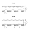
- FIG. 2 is a back plane view illustrating the solar cell 100 according to the embodiment of the invention.
- the configuration of the first and second electrodes 42 and 44 shown in FIG. 2 is provided only as an example and the embodiments of the invention are not limited thereto.
- the doping area 120 is formed to be narrower than the doping layer 20.
- the tunnel junction formed through the tunneling layer 30 between the semiconductor substrate 110 and the doping layer 20 can be widened.
- the base area 110 and the doping area 120 have an n-conductive type and the doping layer 20 has a p-conductive type, holes having a low movement speed can be efficiently collected.
- the doping area 120 may include a first stem portion 120a formed along a first edge (upper edge in the drawing) of the semiconductor substrate 10 and a plurality of first branch portions 120b which extend from the stem portion 120a toward a second edge (lower edge in the drawing) opposite to the first edge.
- the plurality of first branch portions 120b are aligned to be parallel to each other to have a shape of a stripe pattern.
- the doping layer 20 may include a second stem portion 20a formed along the second edge of the semiconductor substrate 110 and a plurality of second branch portions 20b which extend between the first branch portions 120b toward the first edge from the second stem portion 20a.
- the plurality of second branch portions 20b are aligned to be parallel to each other to have a shape of a stripe pattern.
- the first branch portions 120b of the doping area 120 and the second branch portions 20b of the doping layer 20 may be alternately disposed.
- the tunneling layer 30 may have the same shape as or a similar shape to the doping layer 20 and be thus formed to have portions corresponding to the second stem portion 20a and the second branch portion 20b.
- Areas of the doping area 120 and the doping layer 20 may be controlled by varying widths of the first and second stem portions 120a and 20a and/or the first and second branch portions 120b and 20b. That is, the width of the first stem portion 120a may be smaller than that of the second stem portion 20a, and/or the width of the first branch portion 120b may be smaller than that of the second branch portion 20b.
- a ratio of the total area of the doping area 120 to the total area of the solar cell 100 may be 0.5% to 30% (more preferably 0.5% to 5%).
- the ratio of the total area of the doping area 120 is less than 0.5%, contact between the doping area 120 and the first electrode 42 is not accurately formed and contact resistance between the doping area 120 and the first electrode 42 may thus be increased.
- the area ratio exceeds 30%, the area of the doping layer 20 is decreased and efficiency of the solar cell 100 is thus deteriorated, as described above.
- the area ratio is preferably, but not necessarily, 0.5% to 5% in consideration of efficiency of the solar cell.
- the first electrode 42 may include a stem portion 42a corresponding to the first stem portion 120a of the doping area 120 and a branch portion 42b corresponding to the first branch portion 120b of the doping area 120.
- the second electrode 44 may include a stem portion 44a corresponding to the second stem portion 20a of the doping layer 20 and a branch portion 44b corresponding to the second branch portion 20b of the doping layer 20, but the embodiments of the invention are not limited thereto and the first electrode 42 and the second electrode 44 may have a variety of plane shapes.
- the doping area 120 has the first stem portion 120a
- the doping layer 20 has the second stem portion 20a
- the first electrode 42 has the stem portion 42a
- the second electrode 44 has the stem portion 44a.
- the embodiments of the invention are not limited thereto, and the first and second stem portions 120a and 20a, and the stem portions 42a and 44a are not required. Therefore, one or more of the first stem portions 120a, the second stem portion 20a, the stem portion 42a and stem portion 44a may be not formed or may be not included.
- the first electrode 42 entirely contacts a portion of the doping area 120 where the doping layer 20 is not formed, and the second electrode 44 entirely contacts a portion of the doping area 120 where the doping layer 20 is formed. Accordingly, the region of the doping layer 20 is sufficiently secured, and the doping area 120 and the first electrode 42 are spaced from each other, and the doping layer 20 and the second electrode 44 are spaced from each other. As a result, an electrical connection between the doping area 120 and the first electrode 42 and an electrical connection between the doping layer 20 and the second electrode 44 can be stably formed.
- additional layers for insulating the doping area 120 from the first electrode 42 and for insulating the doping layer 20 from the second electrode 44 are not required and structure and manufacturing process can thus be simplified.
- insulating layers for insulating the doping area 120 from the first electrode 42 and the doping layer 20 from the second electrode 44 to improve insulating properties may be formed.
- the doping area 120 corresponding to the back surface field area which may be formed to have a relatively small area is formed on the semiconductor substrate 10 and the doping layer 20 which needs to have a relatively large area is formed on the tunneling layer 30. Based on this configuration, property or characteristics deterioration and damage of the semiconductor substrate 10, which may be generated during doping of the semiconductor substrate 10 with a dopant, can be efficiently prevented or reduced.
- the doping layer 20 and the doping area 120 are separately formed in areas spaced from each other so that a shunt which may be generated when the doping layer 20 is adjacent to the doping area 120 is prevented. For this reason, open-circuit voltage (Voc) and fill factor of the solar cell 100 are increased and efficiency of the solar cell 100 is thus improved.
- the solar cell 100 according to the embodiment may be formed by a variety of methods and the formation method will be described in more detail with reference to FIGS. 3A to 3G , and FIGS. 4A to 4I .
- FIGS. 3A to 3G are sectional views illustrating a method for manufacturing the solar cell according to an embodiment of the invention.
- a semiconductor substrate 10 including a base area 110 having a first conductive-type dopant is prepared in preparation of the substrate.
- the semiconductor substrate 10 may include silicon having an n-type dopant.
- the n-type dopant include Group V elements such as phosphorous (P), arsenic (As), bismuth (Bi) and antimony (Sb).
- the front surface of the semiconductor substrate 10 is textured so that the front surface has irregularities and the back surface of the semiconductor substrate 10 is subjected to treatment such as mirror polishing so that the back surface of the semiconductor substrate 10 has a lower surface roughness than the front surface thereof.
- the back surface may have a flat surface.
- Wet or dry texturing may be used as the texturing of the front surface of the semiconductor substrate 10.
- Wet texturing may be carried out by dipping the semiconductor substrate 10 in a texturing solution and has an advantage of a short process time.
- Dry texturing is a process of cutting the surface of the semiconductor substrate 10 using a diamond drill, laser or the like and enables formation of uniform irregularities, but disadvantageously has a long process time and causes damage to the semiconductor substrate 10.
- the semiconductor substrate 10 may be textured by a reactive ion etching (RIE) or the like.
- RIE reactive ion etching
- the semiconductor substrate 10 may be textured by a variety of methods.
- the back surface of the semiconductor substrate 10 may be treated by a known mirror surface polishing method.
- a tunneling layer 30 and a doping layer 20 are formed on the back surface of the semiconductor substrate 10.
- a barrier layer 22 may be further formed on the doping layer 20.
- the tunneling layer 30 may be formed by a method such as thermal growth or deposition (for example, plasma-enhanced chemical vapor deposition chemical (PECVD), atomic layer deposition (ALD)) or the like, but the embodiments of the invention are not limited thereto and the tunneling layer 30 may be formed by a variety of methods.
- the doping layer 20 includes a microcrystalline, amorphous or polycrystalline semiconductor having a second conductive type dopant.
- the doping layer 20 may be formed by forming a microcrystalline, amorphous or polycrystalline semiconductor by thermal growth, deposition (for example, plasma-enhanced chemical vapor deposition chemical (PECVD)) or the like, and then doping the semiconductor with a second conductive type dopant.
- PECVD plasma-enhanced chemical vapor deposition chemical
- ALD atomic layer deposition
- the doping layer 20 may be formed by doping with the second conductive type dopant while forming a microcrystalline, amorphous or polycrystalline semiconductor through injection of a substance including a second conductive type dopant in the process of thermal growth, deposition (for example, plasma-enhanced chemical vapor deposition chemical (PECVD)) or the like, but the embodiments of the invention are not limited thereto and the semiconductor layer 30 may be formed by a variety of methods.
- PECVD plasma-enhanced chemical vapor deposition chemical
- a mask layer 200 having an opening 200a exposing a region corresponding to the doping area 120 is formed on the doping layer 20.
- the mask layer 200 may be formed by applying a layer including a variety of photoresists, but the embodiments of the invention are not limited thereto and the mask layer 200 may be formed by a variety of methods.
- the doping layer 20, the tunneling layer 30 and the barrier layer 22 are removed from the region corresponding to the opening 200a of the mask layer 200 to form openings 20c and 30c.
- the removal of the doping layer 20 and the tunneling layer 30 of the corresponding region may be carried out using a variety of known methods (for example, etching), but the embodiments of the invention are not limited thereto.
- a doping area 120 is formed in a region corresponding to the openings 20c and 30c by doping a first conductive-type dopant.
- the doping may be carried out using a variety of methods such as ion implantation or thermal diffusion.
- the mask layer 200 may be removed after doping the first conductive-type dopant, but is generally removed after forming the openings 20c and 30c before completion of the formation of the doping area 120 (for example, activated thermal treatment) in order to prevent contamination by the mask layer 200.
- the barrier layer 22 serves as a mask and prevents incorporation of the first conductive-type dopant into the doping layer 20.
- the barrier layer 22 facilitates diffusion of the first conductive-type dopant into the semiconductor substrate 10.
- a front surface field layer 130 is formed on the front surface of the semiconductor substrate 10 and an anti-reflective film 50 is formed thereon.
- the front surface field layer 130 may be formed by doping the semiconductor substrate 10 with a first conductive-type dopant.
- the front surface field layer 130 may be formed by doping the semiconductor substrate 10 with a first conductive-type dopant by a variety of methods such as ion implantation or thermal diffusion.
- the anti-reflective film 50 may be formed by a variety of methods such as vacuum deposition, chemical vapor deposition, spin coating, screen printing or spray coating, but the embodiments of the invention are not limited thereto and various methods may be used.
- first and second electrodes 42 and 44 electrically connected to the doping area 120 and the doping layer 20, respectively, are formed.
- the first electrode 42 is formed by a variety of methods such as coating or deposition after forming an opening in the barrier layer 22.
- the first electrode 42 may be formed by applying a paste for forming the first electrode 42 onto the barrier layer 22 by screen printing or the like and then performing a fire through, a laser firing contact or the like thereon. In this instance, a process of separately forming openings is not required.
- the second electrode 44 may also be formed on the semiconductor substrate 10 (more specifically, on the doping area 120) by a variety of methods such as coating or deposition.
- the tunneling layer 30, the doping layer 20 and the barrier layer 22 are used as masks during formation of the doping area 120, thus advantageously requiring no additional mask process.
- tunneling layer 30, the doping layer 20 and the barrier layer 22 are formed, the doping area 120 is formed, the front surface field layer 130 and the anti-reflective film 50 are formed, and the first and second electrodes 42 and 44 are then formed has been provided in the embodiment above, but the embodiments of the invention are not limited thereto. Accordingly, formation order of the tunneling layer 30, the doping layer 20, the barrier layer 22, the doping area 120, the front surface field layer 130, the anti-reflective film 50, and the first and second electrodes 42 and 44 may be variably changed.
- a method for manufacturing the solar cell 100 according to another embodiment will be described in detail with reference to FIGS. 4A to 4I . Details of the description already given above are not repeated and only difference from the description given above is described in detail.
- FIGS. 4A to 4I are sectional views illustrating a method for manufacturing a solar cell according to another embodiment of the invention.
- a semiconductor substrate 10 including a base area 110 having a first conductive-type dopant is prepared in preparation of the substrate.
- a doping area 20 is formed on the back surface of the semiconductor substrate 10 using a mask 202 having an opening 202a.
- the doping area 120 is formed in the area corresponding to the opening 202a by doping a portion of the back surface of the semiconductor substrate 10 with a first conductive-type dopant while the mask 202 is placed on the back surface.
- the mask 202 is placed on the semiconductor substrate 10 and is, for example, a shadow mask.
- a tunneling layer 30 and a doping layer 20 are formed on the back surface of the semiconductor substrate 10.
- a barrier layer 22 may be further formed on the doping layer 20.
- a mask layer 200 having an opening 200a exposing a region corresponding to the doping area 120 is formed on the doping layer 20.
- the doping layer 20, the tunneling layer 30 and the barrier layer 22 are removed from the region corresponding to the opening 200a of the mask layer 200 to form openings 20c and 30c.
- the mask layer 200 is removed.
- a front surface field layer 130 is formed on the front surface of the semiconductor substrate 10 and an anti-reflective film 50 is formed thereon.
- first and second electrodes 42 and 44 electrically connected to the doping area 120 and the doping layer 20, respectively, are formed.
- the solar cell 100 having the structure can be manufactured by a simple process according to the manufacture method of the solar cell 100, but details of the order and the method may be variably changed as described above.
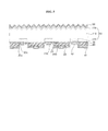
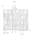
- FIG. 5 is a sectional view illustrating a solar cell according to another embodiment of the invention and FIG. 6 is a back plan view illustrating the solar cell shown in the FIG. 5 .
- the insulating layer 24 is not shown in FIG. 6 .
- the doping area 120 of the embodiment of the invention includes a plurality of first portions 120c connected to the first electrode 42, and the first portions 120c have an island shape.
- an area of the doping area 120 is minimized and the doping area 120 is entirely disposed over the semiconductor substrate 10. That is, surface recombination can be prevented or reduced and an area of the doping layer 20 can be maximized, but the embodiments of the invention are not limited thereto and the doping area 120 may have a variety of shapes capable of minimizing the area of the doping area 120.
- the doping area 120 having a circular shape is shown in the drawing by example, but the embodiments of the invention are not limited thereto. Accordingly, the doping area 120 may have a plane shape including an oval or a polygon, for example, a triangle, rectangle or hexagon.
- a width or diameter of the doping area 120 may be 50 ⁇ m to 1,000 ⁇ m.
- the width or diameter of the doping area 120 is less than 50 ⁇ m, electrical connection between the doping area 120 and the first electrode 42 may not be efficient and when the width or diameter thereof exceeds 1,000 ⁇ m, the area of the doping layer 20 may be decreased or a pitch between the doping area 120 may be increased.
- the width or diameter of the doping area 120 may be 100 ⁇ m to 500 ⁇ m, but the embodiments of the invention are not limited thereto and specific values may be varied according to conditions.
- the doping layer 20 may have an entirely connected to have an integral structure and include an opening (or openings) 20d formed in a region corresponding to the first region 120c. Similar to this, the tunneling layer 30 includes openings 30d corresponding to the first regions 120c and the openings 20d, and the tunneling layer 30 except for the openings 30d is continuously connected between the doping layer and the semiconductor substrate is continuously connected to have an integral structure. When present, the barrier layer 22 may also have an opening in the corresponding region. The openings 20d and 30d of the doping layer 20 and the tunneling layer 30 may be wider than the first region 120c and the first region 120c may be entirely disposed in the openings 20d and 30d, but the embodiments of the invention are not limited thereto and various modifications are possible.
- An insulating layer 24 for insulating the doping area 120 from the doping layer 20 may be formed on the semiconductor substrate 10 including the doping area 120 and the doping layer 20 (or barrier layer 22).
- a first contact hole 24a for connecting the first electrode 42 to the first region 120c of the doping area 120, and a second contact hole 24b for connecting the second electrode 44 to the doping layer 20 may be formed in the insulating layer 24.
- the first contact hole 24a may be formed to have an island shape in a region that corresponds to the first region 120c and the second contact hole 24b may have a shape entirely the same as or similar to the second electrode 44 according to the shape of the second electrode 44.
- the second contact hole 24b may have portions corresponding to the stem portion 44a and the branch portion 44b.
- the first contact hole 24a and the second contact hole 24b may have different shapes in consideration of the doping area 120 having an island region and the entirely connected shape of the doping layer 20.
- electrical connection of the first electrode 42 and the doping area 120 having an island shape is efficiently secured, and insulation between the first electrode 42 and the doping layer 20 is stably maintained.
- the second electrode 44 entirely contacts the doping layer 20, thereby improving carrier resin efficiency, but the embodiments of the invention are not limited thereto and shapes of the first and second contact holes 24a and 24b may be changed.
- first electrode 42 has the same shape as in the embodiment shown in FIG. 1 has been given in the embodiment of the invention, but the shape of the first electrode 42 or the like may be varied. A modified embodiment will be described with reference to FIG. 7 .
- FIG. 7 is a back plan view illustrating a solar cell according to the modified embodiment of the invention.
- the branch portion 42b of the first electrode 42 may include a plurality of first portions 421b corresponding to the first region 120c of the doping area 120, and a second portion 422b which connects the first portions 421b to one another and has a smaller width than each first portion 421b. That is, the width of the first portion 421b corresponding to the first region 120c is greater than widths of other portions, thereby sufficiently securing areas of the respective first portions 120c, or areas of contact holes 24 connecting the first electrode 42 to the first region 120c. As a result, electrical connection between the first electrode 42 and the first region 120c can be further facilitated.
- FIGS. 5 to 7 The method for manufacturing the solar cell 100 shown in FIGS. 5 to 7 will be described in detail with reference to FIGS. 8A to 8C .
- Contents of the embodiments that are the same as or similar to the embodiment described above are not described in detail with reference to FIGS. 3A to 3G , and FIGS. 4A to 4I and only contents different from those described above are described.
- FIGS. 8A to 8C are sectional views illustrating a method for manufacturing a solar cell according to another embodiment of the invention.
- a doping area 120 is formed on the semiconductor substrate 10 and a tunneling layer 30, a doping layer 20 and a barrier layer 22 having openings 30d and 20d are formed on the semiconductor substrate 10.
- an insulating layer 24 is formed over the entire surface of the structure including the semiconductor substrate 10, the tunneling layer 30, the doping layer 20 and the barrier layer 22.
- the insulating layer 24 may include a variety of insulating materials (for example, oxides, nitrides or the like) and may be formed by a variety of methods such as vacuum deposition, chemical vapor deposition, spin coating, screen printing or spray coating, but the embodiments of the invention are not limited thereto and various methods may be used.
- a front surface field layer 130 and an anti-reflective film 50 are formed on the front surface of the semiconductor substrate 110.
- first and second electrodes 42 and 44 electrically connected to the doping area 120 and the doping layer 20 through a first contact hole 24a and a second contact hole 24b are formed.
- the solar cell 100 having the structure described above can be formed by such a manufacturing method.
- FIG. 9 is a sectional view illustrating a solar cell according to another embodiment of the invention.
- the semiconductor substrate 10 includes only the base area 110 and does not include an additional front surface field layer (represented by reference numeral "130" in FIG. 1 , the same will be applied below). Instead, a field effect-forming layer 52 which contacts the base area 110 of the semiconductor substrate 10 and has a fixed charge is formed. Similar to the front surface field layer 130, the field effect-forming layer 52 generates a certain field effect and thereby prevents or reduces surface recombination.
- the field effect-forming layer 52 may be composed of aluminum oxide having a negative charge, or silicon oxide or silicon nitride having a positive charge or the like.
- an additional anti-reflective film represented by reference numeral "50" in FIG. 1 ) may be further formed on the field effect-forming layer 52.
- the area of the doping area formed in the semiconductor substrate 10 is greatly reduced and the overall process is thus simplified.
- damage to the semiconductor substrate 10 which may be generated during formation of the doping area can be efficiently reduced.
- an amount of fixed charges of the field effect-forming layer 52 is for example, 1 X 10 12 /cm 2 to 9 X 10 13 /cm 2 .
- the amount of the fixed charges is a level enabling generation of the field effect in the semiconductor substrate 10 not including the doping area. More specifically, in consideration of the field effect, the amount of fixed charges may be 1 X 10 12 /cm 2 to 1 X 10 13 /cm 2 , but the embodiments of the invention are not limited thereto and the amount of fixed charges may be varied.
- the base area 110 not including the doping area may have a specific resistance of 0.5 ohm ⁇ cm to 20 ohm ⁇ cm (for example, 1 ohm ⁇ cm to 15 ohm ⁇ cm). Accordingly, in a region adjacent to the field effect-forming layer 52, the semiconductor substrate 10 may have a specific resistance of 0.5 ohm ⁇ cm to 20 ohm ⁇ cm (for example, 1 ohm ⁇ cm to 15 ohm ⁇ cm).
- this specific resistance range is given as an example of an instance when the semiconductor substrate 10 includes an n-type base area 110 using phosphorous (P) as a dopant and may be changed according to conductive type, dopant type or the like.
Landscapes
- Photovoltaic Devices (AREA)
- Life Sciences & Earth Sciences (AREA)
- Engineering & Computer Science (AREA)
- Sustainable Energy (AREA)
- Sustainable Development (AREA)
- Manufacturing & Machinery (AREA)
- Chemical & Material Sciences (AREA)
- Crystallography & Structural Chemistry (AREA)
Applications Claiming Priority (1)
| Application Number | Priority Date | Filing Date | Title |
|---|---|---|---|
| KR1020130055756A KR20140135881A (ko) | 2013-05-16 | 2013-05-16 | 태양 전지 및 이의 제조 방법 |
Publications (2)
| Publication Number | Publication Date |
|---|---|
| EP2804219A1 true EP2804219A1 (de) | 2014-11-19 |
| EP2804219B1 EP2804219B1 (de) | 2019-10-16 |
Family
ID=50732751
Family Applications (1)
| Application Number | Title | Priority Date | Filing Date |
|---|---|---|---|
| EP14001746.8A Active EP2804219B1 (de) | 2013-05-16 | 2014-05-16 | Solarzelle und verfahren zu ihrer herstellung |
Country Status (4)
| Country | Link |
|---|---|
| US (1) | US10566484B2 (de) |
| EP (1) | EP2804219B1 (de) |
| KR (1) | KR20140135881A (de) |
| CN (1) | CN104167454B (de) |
Cited By (3)
| Publication number | Priority date | Publication date | Assignee | Title |
|---|---|---|---|---|
| CN109983584A (zh) * | 2016-11-25 | 2019-07-05 | 荷兰应用自然科学研究组织 Tno | 具有钝化接触的光伏电池 |
| WO2021223932A1 (de) * | 2020-05-04 | 2021-11-11 | EnPV GmbH | Rückseitenkontaktierte solarzelle |
| EP4694629A1 (de) * | 2024-08-09 | 2026-02-11 | CSI Cells (YangZhou) Co., Ltd. | Solarzelle |
Families Citing this family (22)
| Publication number | Priority date | Publication date | Assignee | Title |
|---|---|---|---|---|
| DE102013100818B4 (de) * | 2013-01-28 | 2023-07-27 | OSRAM Opto Semiconductors Gesellschaft mit beschränkter Haftung | Optoelektronischer Halbleiterchip und Verfahren zur Herstellung eines optoelektronischen Halbleiterchips |
| CN104282788B (zh) * | 2014-09-28 | 2017-03-22 | 苏州中来光伏新材股份有限公司 | 无主栅、高效率背接触太阳能电池模块、组件及制备工艺 |
| KR102317141B1 (ko) * | 2015-02-10 | 2021-10-22 | 엘지전자 주식회사 | 태양 전지 |
| KR102373649B1 (ko) | 2015-05-28 | 2022-03-11 | 엘지전자 주식회사 | 태양 전지 및 이의 제조 방법 |
| NL2015533B1 (en) * | 2015-09-30 | 2017-04-20 | Tempress Ip B V | Method of manufacturing of a solar cell and solar cell thus obtained. |
| WO2018032351A1 (en) | 2016-08-16 | 2018-02-22 | Zhejiang Kaiying New Materials Co., Ltd. | Thick-film paste for front-side metallization in silicon solar cells |
| CN108885917B (zh) | 2016-12-20 | 2020-06-02 | 浙江凯盈新材料有限公司 | 含硅氧烷的太阳能电池金属化浆料 |
| CN108575097B (zh) | 2016-12-20 | 2021-08-17 | 浙江凯盈新材料有限公司 | 具有印刷的氧化物隧道结的叉指背接触金属-绝缘体-半导体太阳能电池 |
| US20200279968A1 (en) * | 2017-09-22 | 2020-09-03 | Nederlandse Organisatie Voor Toegepast-Natuurwetenschappelijk Onderzoek Tno | Interdigitated back-contacted solar cell with p-type conductivity |
| CN108666377A (zh) * | 2018-07-11 | 2018-10-16 | 泰州隆基乐叶光伏科技有限公司 | 一种p型背接触太阳电池及其制备方法 |
| JP7346050B2 (ja) * | 2019-03-26 | 2023-09-19 | パナソニックホールディングス株式会社 | 太陽電池セルおよび太陽電池モジュール |
| CN110061086A (zh) * | 2019-04-04 | 2019-07-26 | 国家电投集团西安太阳能电力有限公司 | 一种hbc太阳能电池 |
| US10622502B1 (en) | 2019-05-23 | 2020-04-14 | Zhejiang Kaiying New Materials Co., Ltd. | Solar cell edge interconnects |
| US10749045B1 (en) | 2019-05-23 | 2020-08-18 | Zhejiang Kaiying New Materials Co., Ltd. | Solar cell side surface interconnects |
| DE102019122637B4 (de) * | 2019-08-22 | 2022-11-03 | Fraunhofer-Gesellschaft zur Förderung der angewandten Forschung e.V. | Verfahren zur Herstellung einer metallischen Kontaktierungsstruktur einer photovoltaischen Solarzelle |
| US11824126B2 (en) * | 2019-12-10 | 2023-11-21 | Maxeon Solar Pte. Ltd. | Aligned metallization for solar cells |
| FR3112427A1 (fr) * | 2020-07-13 | 2022-01-14 | Semco Smartech France | Formation de contacts passivés pour cellules solaires IBC |
| DE102020132245A1 (de) * | 2020-12-04 | 2022-06-09 | EnPV GmbH | Rückseitenkontaktierte Solarzelle und Herstellung einer solchen |
| CN114361268A (zh) * | 2021-12-29 | 2022-04-15 | 中国建材国际工程集团有限公司 | 一种背接触CdTe太阳电池及其制造方法 |
| CN118156325A (zh) | 2022-12-07 | 2024-06-07 | 浙江晶科能源有限公司 | 太阳能电池及光伏组件 |
| CN119008711A (zh) | 2023-10-13 | 2024-11-22 | 浙江晶科能源有限公司 | 太阳能电池及其制备方法、光伏组件 |
| CN119008712A (zh) * | 2023-10-13 | 2024-11-22 | 浙江晶科能源有限公司 | 太阳能电池及光伏组件 |
Citations (4)
| Publication number | Priority date | Publication date | Assignee | Title |
|---|---|---|---|---|
| WO2010142684A2 (de) * | 2009-06-10 | 2010-12-16 | Institut für Solarenergieforschung | Solarzelle mit kontaktstruktur mit geringen rekombinationsverlusten sowie herstellungsverfahren für solche solarzellen |
| US20120291860A1 (en) * | 2011-05-19 | 2012-11-22 | Min Park | Solar cell and method of manufacturing the same |
| CN103107228A (zh) * | 2011-11-10 | 2013-05-15 | 株式会社半导体能源研究所 | 光电转换装置 |
| WO2013161145A1 (ja) * | 2012-04-27 | 2013-10-31 | パナソニック株式会社 | 裏面接合型太陽電池及びその製造方法 |
Family Cites Families (14)
| Publication number | Priority date | Publication date | Assignee | Title |
|---|---|---|---|---|
| US4496788A (en) * | 1982-12-29 | 1985-01-29 | Osaka Transformer Co., Ltd. | Photovoltaic device |
| JP3203078B2 (ja) * | 1992-12-09 | 2001-08-27 | 三洋電機株式会社 | 光起電力素子 |
| US6111189A (en) * | 1998-07-28 | 2000-08-29 | Bp Solarex | Photovoltaic module framing system with integral electrical raceways |
| JP3490964B2 (ja) * | 2000-09-05 | 2004-01-26 | 三洋電機株式会社 | 光起電力装置 |
| WO2003047005A2 (en) * | 2001-11-26 | 2003-06-05 | Shell Solar Gmbh | Manufacturing a solar cell with backside contacts |
| US20110000532A1 (en) * | 2008-01-30 | 2011-01-06 | Kyocera Corporation | Solar Cell Device and Method of Manufacturing Solar Cell Device |
| US20120037224A1 (en) | 2009-04-29 | 2012-02-16 | Mitsubishi Electric Corporation | Solar battery cell and method of manufacturing the same |
| US8735234B2 (en) * | 2010-02-18 | 2014-05-27 | Varian Semiconductor Equipment Associates, Inc. | Self-aligned ion implantation for IBC solar cells |
| KR20130056364A (ko) * | 2010-04-23 | 2013-05-29 | 솔렉셀, 인크. | 고효율 태양 전지 극 저 표면 재결합 속도를 달성하기 위한 패시베이션 방법 및 장치 |
| EP2395554A3 (de) * | 2010-06-14 | 2015-03-11 | Imec | Herstellungsverfahren für ineinandergreifende Rückkontakt-Photovoltaikzellen |
| KR101773837B1 (ko) * | 2011-01-21 | 2017-09-01 | 엘지전자 주식회사 | 태양전지 및 그 제조방법 |
| KR20120086593A (ko) | 2011-01-26 | 2012-08-03 | 엘지전자 주식회사 | 태양전지 및 그 제조방법 |
| NL2006932C2 (en) | 2011-06-14 | 2012-12-17 | Stichting Energie | Photovoltaic cell. |
| CN102856328B (zh) * | 2012-10-10 | 2015-06-10 | 友达光电股份有限公司 | 太阳能电池及其制作方法 |
-
2013
- 2013-05-16 KR KR1020130055756A patent/KR20140135881A/ko not_active Ceased
-
2014
- 2014-05-15 US US14/278,827 patent/US10566484B2/en active Active
- 2014-05-16 CN CN201410354042.5A patent/CN104167454B/zh not_active Expired - Fee Related
- 2014-05-16 EP EP14001746.8A patent/EP2804219B1/de active Active
Patent Citations (5)
| Publication number | Priority date | Publication date | Assignee | Title |
|---|---|---|---|---|
| WO2010142684A2 (de) * | 2009-06-10 | 2010-12-16 | Institut für Solarenergieforschung | Solarzelle mit kontaktstruktur mit geringen rekombinationsverlusten sowie herstellungsverfahren für solche solarzellen |
| US20120291860A1 (en) * | 2011-05-19 | 2012-11-22 | Min Park | Solar cell and method of manufacturing the same |
| CN103107228A (zh) * | 2011-11-10 | 2013-05-15 | 株式会社半导体能源研究所 | 光电转换装置 |
| US20130119374A1 (en) * | 2011-11-10 | 2013-05-16 | Semiconductor Energy Laboratory Co., Ltd. | Photoelectric conversion device |
| WO2013161145A1 (ja) * | 2012-04-27 | 2013-10-31 | パナソニック株式会社 | 裏面接合型太陽電池及びその製造方法 |
Cited By (3)
| Publication number | Priority date | Publication date | Assignee | Title |
|---|---|---|---|---|
| CN109983584A (zh) * | 2016-11-25 | 2019-07-05 | 荷兰应用自然科学研究组织 Tno | 具有钝化接触的光伏电池 |
| WO2021223932A1 (de) * | 2020-05-04 | 2021-11-11 | EnPV GmbH | Rückseitenkontaktierte solarzelle |
| EP4694629A1 (de) * | 2024-08-09 | 2026-02-11 | CSI Cells (YangZhou) Co., Ltd. | Solarzelle |
Also Published As
| Publication number | Publication date |
|---|---|
| US10566484B2 (en) | 2020-02-18 |
| US20140338747A1 (en) | 2014-11-20 |
| CN104167454B (zh) | 2017-10-13 |
| EP2804219B1 (de) | 2019-10-16 |
| KR20140135881A (ko) | 2014-11-27 |
| CN104167454A (zh) | 2014-11-26 |
Similar Documents
| Publication | Publication Date | Title |
|---|---|---|
| US10566484B2 (en) | Solar cell and method for manufacturing the same | |
| US20230023777A1 (en) | Solar cell | |
| US10854764B2 (en) | Solar cell and method for manufacturing the same | |
| US9356182B2 (en) | Solar cell and method of manufacturing the same | |
| EP2822041B1 (de) | Solarzelle und Verfahren zu ihrer Herstellung | |
| US10424681B2 (en) | Solar cell | |
| KR102244838B1 (ko) | 태양 전지 및 이의 제조 방법 | |
| KR102053140B1 (ko) | 태양 전지 | |
| US10141467B2 (en) | Solar cell and method for manufacturing the same | |
| KR20150049211A (ko) | 태양 전지 및 이의 제조 방법 | |
| US9640707B2 (en) | Method of manufacturing solar cell and method of forming doping region | |
| KR102298671B1 (ko) | 태양 전지 및 이의 제조 방법 | |
| KR102132741B1 (ko) | 태양 전지 및 이의 제조 방법 | |
| KR20160061947A (ko) | 태양 전지 및 이의 제조 방법 | |
| KR20150011119A (ko) | 태양 전지의 제조 방법 |
Legal Events
| Date | Code | Title | Description |
|---|---|---|---|
| PUAI | Public reference made under article 153(3) epc to a published international application that has entered the european phase |
Free format text: ORIGINAL CODE: 0009012 |
|
| 17P | Request for examination filed |
Effective date: 20140516 |
|
| AK | Designated contracting states |
Kind code of ref document: A1 Designated state(s): AL AT BE BG CH CY CZ DE DK EE ES FI FR GB GR HR HU IE IS IT LI LT LU LV MC MK MT NL NO PL PT RO RS SE SI SK SM TR |
|
| AX | Request for extension of the european patent |
Extension state: BA ME |
|
| STAA | Information on the status of an ep patent application or granted ep patent |
Free format text: STATUS: EXAMINATION IS IN PROGRESS |
|
| 17Q | First examination report despatched |
Effective date: 20170109 |
|
| REG | Reference to a national code |
Ref country code: DE Ref legal event code: R079 Ref document number: 602014055124 Country of ref document: DE Free format text: PREVIOUS MAIN CLASS: H01L0031022400 Ipc: H01L0031068000 |
|
| GRAJ | Information related to disapproval of communication of intention to grant by the applicant or resumption of examination proceedings by the epo deleted |
Free format text: ORIGINAL CODE: EPIDOSDIGR1 |
|
| STAA | Information on the status of an ep patent application or granted ep patent |
Free format text: STATUS: GRANT OF PATENT IS INTENDED |
|
| RIC1 | Information provided on ipc code assigned before grant |
Ipc: H01L 31/0747 20120101ALI20190416BHEP Ipc: H01L 31/068 20120101AFI20190416BHEP Ipc: H01L 31/0224 20060101ALI20190416BHEP Ipc: H01L 31/18 20060101ALI20190416BHEP |
|
| GRAP | Despatch of communication of intention to grant a patent |
Free format text: ORIGINAL CODE: EPIDOSNIGR1 |
|
| INTG | Intention to grant announced |
Effective date: 20190529 |
|
| RIN1 | Information on inventor provided before grant (corrected) |
Inventor name: PARK, HYUNJUNG Inventor name: CHOE, YOUNGHO Inventor name: CHOI, MINHO Inventor name: CHOI, JUNGHOON |
|
| GRAS | Grant fee paid |
Free format text: ORIGINAL CODE: EPIDOSNIGR3 |
|
| GRAA | (expected) grant |
Free format text: ORIGINAL CODE: 0009210 |
|
| STAA | Information on the status of an ep patent application or granted ep patent |
Free format text: STATUS: THE PATENT HAS BEEN GRANTED |
|
| AK | Designated contracting states |
Kind code of ref document: B1 Designated state(s): AL AT BE BG CH CY CZ DE DK EE ES FI FR GB GR HR HU IE IS IT LI LT LU LV MC MK MT NL NO PL PT RO RS SE SI SK SM TR |
|
| REG | Reference to a national code |
Ref country code: GB Ref legal event code: FG4D |
|
| REG | Reference to a national code |
Ref country code: CH Ref legal event code: EP |
|
| REG | Reference to a national code |
Ref country code: DE Ref legal event code: R096 Ref document number: 602014055124 Country of ref document: DE |
|
| REG | Reference to a national code |
Ref country code: IE Ref legal event code: FG4D |
|
| REG | Reference to a national code |
Ref country code: AT Ref legal event code: REF Ref document number: 1192141 Country of ref document: AT Kind code of ref document: T Effective date: 20191115 |
|
| REG | Reference to a national code |
Ref country code: NL Ref legal event code: MP Effective date: 20191016 |
|
| REG | Reference to a national code |
Ref country code: LT Ref legal event code: MG4D |
|
| REG | Reference to a national code |
Ref country code: AT Ref legal event code: MK05 Ref document number: 1192141 Country of ref document: AT Kind code of ref document: T Effective date: 20191016 |
|
| PG25 | Lapsed in a contracting state [announced via postgrant information from national office to epo] |
Ref country code: NL Free format text: LAPSE BECAUSE OF FAILURE TO SUBMIT A TRANSLATION OF THE DESCRIPTION OR TO PAY THE FEE WITHIN THE PRESCRIBED TIME-LIMIT Effective date: 20191016 Ref country code: AT Free format text: LAPSE BECAUSE OF FAILURE TO SUBMIT A TRANSLATION OF THE DESCRIPTION OR TO PAY THE FEE WITHIN THE PRESCRIBED TIME-LIMIT Effective date: 20191016 Ref country code: BG Free format text: LAPSE BECAUSE OF FAILURE TO SUBMIT A TRANSLATION OF THE DESCRIPTION OR TO PAY THE FEE WITHIN THE PRESCRIBED TIME-LIMIT Effective date: 20200116 Ref country code: FI Free format text: LAPSE BECAUSE OF FAILURE TO SUBMIT A TRANSLATION OF THE DESCRIPTION OR TO PAY THE FEE WITHIN THE PRESCRIBED TIME-LIMIT Effective date: 20191016 Ref country code: LT Free format text: LAPSE BECAUSE OF FAILURE TO SUBMIT A TRANSLATION OF THE DESCRIPTION OR TO PAY THE FEE WITHIN THE PRESCRIBED TIME-LIMIT Effective date: 20191016 Ref country code: PT Free format text: LAPSE BECAUSE OF FAILURE TO SUBMIT A TRANSLATION OF THE DESCRIPTION OR TO PAY THE FEE WITHIN THE PRESCRIBED TIME-LIMIT Effective date: 20200217 Ref country code: SE Free format text: LAPSE BECAUSE OF FAILURE TO SUBMIT A TRANSLATION OF THE DESCRIPTION OR TO PAY THE FEE WITHIN THE PRESCRIBED TIME-LIMIT Effective date: 20191016 Ref country code: LV Free format text: LAPSE BECAUSE OF FAILURE TO SUBMIT A TRANSLATION OF THE DESCRIPTION OR TO PAY THE FEE WITHIN THE PRESCRIBED TIME-LIMIT Effective date: 20191016 Ref country code: NO Free format text: LAPSE BECAUSE OF FAILURE TO SUBMIT A TRANSLATION OF THE DESCRIPTION OR TO PAY THE FEE WITHIN THE PRESCRIBED TIME-LIMIT Effective date: 20200116 Ref country code: GR Free format text: LAPSE BECAUSE OF FAILURE TO SUBMIT A TRANSLATION OF THE DESCRIPTION OR TO PAY THE FEE WITHIN THE PRESCRIBED TIME-LIMIT Effective date: 20200117 Ref country code: PL Free format text: LAPSE BECAUSE OF FAILURE TO SUBMIT A TRANSLATION OF THE DESCRIPTION OR TO PAY THE FEE WITHIN THE PRESCRIBED TIME-LIMIT Effective date: 20191016 |
|
| PG25 | Lapsed in a contracting state [announced via postgrant information from national office to epo] |
Ref country code: RS Free format text: LAPSE BECAUSE OF FAILURE TO SUBMIT A TRANSLATION OF THE DESCRIPTION OR TO PAY THE FEE WITHIN THE PRESCRIBED TIME-LIMIT Effective date: 20191016 Ref country code: HR Free format text: LAPSE BECAUSE OF FAILURE TO SUBMIT A TRANSLATION OF THE DESCRIPTION OR TO PAY THE FEE WITHIN THE PRESCRIBED TIME-LIMIT Effective date: 20191016 Ref country code: IS Free format text: LAPSE BECAUSE OF FAILURE TO SUBMIT A TRANSLATION OF THE DESCRIPTION OR TO PAY THE FEE WITHIN THE PRESCRIBED TIME-LIMIT Effective date: 20200224 |
|
| PG25 | Lapsed in a contracting state [announced via postgrant information from national office to epo] |
Ref country code: AL Free format text: LAPSE BECAUSE OF FAILURE TO SUBMIT A TRANSLATION OF THE DESCRIPTION OR TO PAY THE FEE WITHIN THE PRESCRIBED TIME-LIMIT Effective date: 20191016 |
|
| REG | Reference to a national code |
Ref country code: DE Ref legal event code: R097 Ref document number: 602014055124 Country of ref document: DE |
|
| PG2D | Information on lapse in contracting state deleted |
Ref country code: IS |
|
| PG25 | Lapsed in a contracting state [announced via postgrant information from national office to epo] |
Ref country code: RO Free format text: LAPSE BECAUSE OF FAILURE TO SUBMIT A TRANSLATION OF THE DESCRIPTION OR TO PAY THE FEE WITHIN THE PRESCRIBED TIME-LIMIT Effective date: 20191016 Ref country code: CZ Free format text: LAPSE BECAUSE OF FAILURE TO SUBMIT A TRANSLATION OF THE DESCRIPTION OR TO PAY THE FEE WITHIN THE PRESCRIBED TIME-LIMIT Effective date: 20191016 Ref country code: ES Free format text: LAPSE BECAUSE OF FAILURE TO SUBMIT A TRANSLATION OF THE DESCRIPTION OR TO PAY THE FEE WITHIN THE PRESCRIBED TIME-LIMIT Effective date: 20191016 Ref country code: EE Free format text: LAPSE BECAUSE OF FAILURE TO SUBMIT A TRANSLATION OF THE DESCRIPTION OR TO PAY THE FEE WITHIN THE PRESCRIBED TIME-LIMIT Effective date: 20191016 Ref country code: DK Free format text: LAPSE BECAUSE OF FAILURE TO SUBMIT A TRANSLATION OF THE DESCRIPTION OR TO PAY THE FEE WITHIN THE PRESCRIBED TIME-LIMIT Effective date: 20191016 Ref country code: IS Free format text: LAPSE BECAUSE OF FAILURE TO SUBMIT A TRANSLATION OF THE DESCRIPTION OR TO PAY THE FEE WITHIN THE PRESCRIBED TIME-LIMIT Effective date: 20200216 |
|
| PLBE | No opposition filed within time limit |
Free format text: ORIGINAL CODE: 0009261 |
|
| STAA | Information on the status of an ep patent application or granted ep patent |
Free format text: STATUS: NO OPPOSITION FILED WITHIN TIME LIMIT |
|
| PG25 | Lapsed in a contracting state [announced via postgrant information from national office to epo] |
Ref country code: SM Free format text: LAPSE BECAUSE OF FAILURE TO SUBMIT A TRANSLATION OF THE DESCRIPTION OR TO PAY THE FEE WITHIN THE PRESCRIBED TIME-LIMIT Effective date: 20191016 Ref country code: SK Free format text: LAPSE BECAUSE OF FAILURE TO SUBMIT A TRANSLATION OF THE DESCRIPTION OR TO PAY THE FEE WITHIN THE PRESCRIBED TIME-LIMIT Effective date: 20191016 Ref country code: IT Free format text: LAPSE BECAUSE OF FAILURE TO SUBMIT A TRANSLATION OF THE DESCRIPTION OR TO PAY THE FEE WITHIN THE PRESCRIBED TIME-LIMIT Effective date: 20191016 |
|
| 26N | No opposition filed |
Effective date: 20200717 |
|
| PG25 | Lapsed in a contracting state [announced via postgrant information from national office to epo] |
Ref country code: SI Free format text: LAPSE BECAUSE OF FAILURE TO SUBMIT A TRANSLATION OF THE DESCRIPTION OR TO PAY THE FEE WITHIN THE PRESCRIBED TIME-LIMIT Effective date: 20191016 |
|
| REG | Reference to a national code |
Ref country code: DE Ref legal event code: R119 Ref document number: 602014055124 Country of ref document: DE |
|
| PG25 | Lapsed in a contracting state [announced via postgrant information from national office to epo] |
Ref country code: CH Free format text: LAPSE BECAUSE OF NON-PAYMENT OF DUE FEES Effective date: 20200531 Ref country code: MC Free format text: LAPSE BECAUSE OF FAILURE TO SUBMIT A TRANSLATION OF THE DESCRIPTION OR TO PAY THE FEE WITHIN THE PRESCRIBED TIME-LIMIT Effective date: 20191016 Ref country code: LI Free format text: LAPSE BECAUSE OF NON-PAYMENT OF DUE FEES Effective date: 20200531 |
|
| REG | Reference to a national code |
Ref country code: BE Ref legal event code: MM Effective date: 20200531 |
|
| GBPC | Gb: european patent ceased through non-payment of renewal fee |
Effective date: 20200516 |
|
| PG25 | Lapsed in a contracting state [announced via postgrant information from national office to epo] |
Ref country code: LU Free format text: LAPSE BECAUSE OF NON-PAYMENT OF DUE FEES Effective date: 20200516 |
|
| PG25 | Lapsed in a contracting state [announced via postgrant information from national office to epo] |
Ref country code: IE Free format text: LAPSE BECAUSE OF NON-PAYMENT OF DUE FEES Effective date: 20200516 Ref country code: GB Free format text: LAPSE BECAUSE OF NON-PAYMENT OF DUE FEES Effective date: 20200516 Ref country code: FR Free format text: LAPSE BECAUSE OF NON-PAYMENT OF DUE FEES Effective date: 20200531 |
|
| PG25 | Lapsed in a contracting state [announced via postgrant information from national office to epo] |
Ref country code: BE Free format text: LAPSE BECAUSE OF NON-PAYMENT OF DUE FEES Effective date: 20200531 Ref country code: DE Free format text: LAPSE BECAUSE OF NON-PAYMENT OF DUE FEES Effective date: 20201201 |
|
| PG25 | Lapsed in a contracting state [announced via postgrant information from national office to epo] |
Ref country code: TR Free format text: LAPSE BECAUSE OF FAILURE TO SUBMIT A TRANSLATION OF THE DESCRIPTION OR TO PAY THE FEE WITHIN THE PRESCRIBED TIME-LIMIT Effective date: 20191016 Ref country code: MT Free format text: LAPSE BECAUSE OF FAILURE TO SUBMIT A TRANSLATION OF THE DESCRIPTION OR TO PAY THE FEE WITHIN THE PRESCRIBED TIME-LIMIT Effective date: 20191016 Ref country code: CY Free format text: LAPSE BECAUSE OF FAILURE TO SUBMIT A TRANSLATION OF THE DESCRIPTION OR TO PAY THE FEE WITHIN THE PRESCRIBED TIME-LIMIT Effective date: 20191016 |
|
| PG25 | Lapsed in a contracting state [announced via postgrant information from national office to epo] |
Ref country code: MK Free format text: LAPSE BECAUSE OF FAILURE TO SUBMIT A TRANSLATION OF THE DESCRIPTION OR TO PAY THE FEE WITHIN THE PRESCRIBED TIME-LIMIT Effective date: 20191016 |