EP2804221A1 - Solarzelle aus einer cigs-verbindung - Google Patents
Solarzelle aus einer cigs-verbindung Download PDFInfo
- Publication number
- EP2804221A1 EP2804221A1 EP13755506.6A EP13755506A EP2804221A1 EP 2804221 A1 EP2804221 A1 EP 2804221A1 EP 13755506 A EP13755506 A EP 13755506A EP 2804221 A1 EP2804221 A1 EP 2804221A1
- Authority
- EP
- European Patent Office
- Prior art keywords
- cigs
- plane
- peak intensity
- buffer layer
- solar cell
- Prior art date
- Legal status (The legal status is an assumption and is not a legal conclusion. Google has not performed a legal analysis and makes no representation as to the accuracy of the status listed.)
- Granted
Links
- 239000000758 substrate Substances 0.000 claims abstract description 35
- 150000001875 compounds Chemical class 0.000 claims abstract description 30
- 239000013078 crystal Substances 0.000 claims abstract description 28
- 238000002441 X-ray diffraction Methods 0.000 claims abstract description 27
- XLOMVQKBTHCTTD-UHFFFAOYSA-N Zinc monoxide Chemical compound [Zn]=O XLOMVQKBTHCTTD-UHFFFAOYSA-N 0.000 claims abstract description 20
- 239000011787 zinc oxide Substances 0.000 claims abstract description 10
- 239000002184 metal Substances 0.000 claims abstract description 9
- 229910044991 metal oxide Inorganic materials 0.000 claims abstract description 6
- 150000004706 metal oxides Chemical class 0.000 claims abstract description 6
- 239000004065 semiconductor Substances 0.000 claims description 12
- 238000006243 chemical reaction Methods 0.000 abstract description 27
- 239000010410 layer Substances 0.000 description 130
- 229910017612 Cu(In,Ga)Se2 Inorganic materials 0.000 description 65
- 230000000052 comparative effect Effects 0.000 description 26
- 238000004544 sputter deposition Methods 0.000 description 23
- 230000015572 biosynthetic process Effects 0.000 description 15
- 238000000034 method Methods 0.000 description 11
- 239000010949 copper Substances 0.000 description 9
- XKRFYHLGVUSROY-UHFFFAOYSA-N Argon Chemical compound [Ar] XKRFYHLGVUSROY-UHFFFAOYSA-N 0.000 description 8
- 239000011521 glass Substances 0.000 description 7
- 238000007740 vapor deposition Methods 0.000 description 7
- 239000007789 gas Substances 0.000 description 6
- 238000001755 magnetron sputter deposition Methods 0.000 description 6
- 239000000203 mixture Substances 0.000 description 6
- 239000011669 selenium Substances 0.000 description 5
- 229910052786 argon Inorganic materials 0.000 description 4
- 229910052733 gallium Inorganic materials 0.000 description 4
- 229910052738 indium Inorganic materials 0.000 description 4
- 238000005259 measurement Methods 0.000 description 4
- 239000010409 thin film Substances 0.000 description 4
- 239000011701 zinc Substances 0.000 description 4
- 239000011651 chromium Substances 0.000 description 3
- 239000010408 film Substances 0.000 description 3
- 229910052751 metal Inorganic materials 0.000 description 3
- 239000003513 alkali Substances 0.000 description 2
- 229910052783 alkali metal Inorganic materials 0.000 description 2
- 230000004888 barrier function Effects 0.000 description 2
- 230000005540 biological transmission Effects 0.000 description 2
- DVRDHUBQLOKMHZ-UHFFFAOYSA-N chalcopyrite Chemical group [S-2].[S-2].[Fe+2].[Cu+2] DVRDHUBQLOKMHZ-UHFFFAOYSA-N 0.000 description 2
- 238000005234 chemical deposition Methods 0.000 description 2
- 238000005229 chemical vapour deposition Methods 0.000 description 2
- 229910052802 copper Inorganic materials 0.000 description 2
- 230000007547 defect Effects 0.000 description 2
- 238000009792 diffusion process Methods 0.000 description 2
- 238000000605 extraction Methods 0.000 description 2
- PJXISJQVUVHSOJ-UHFFFAOYSA-N indium(III) oxide Inorganic materials [O-2].[O-2].[O-2].[In+3].[In+3] PJXISJQVUVHSOJ-UHFFFAOYSA-N 0.000 description 2
- 239000000463 material Substances 0.000 description 2
- 229910052750 molybdenum Inorganic materials 0.000 description 2
- 229910052760 oxygen Inorganic materials 0.000 description 2
- 239000011347 resin Substances 0.000 description 2
- 229920005989 resin Polymers 0.000 description 2
- 238000005096 rolling process Methods 0.000 description 2
- 229910052711 selenium Inorganic materials 0.000 description 2
- 239000002356 single layer Substances 0.000 description 2
- 239000005361 soda-lime glass Substances 0.000 description 2
- 238000005477 sputtering target Methods 0.000 description 2
- 229910052717 sulfur Inorganic materials 0.000 description 2
- XOLBLPGZBRYERU-UHFFFAOYSA-N tin dioxide Chemical compound O=[Sn]=O XOLBLPGZBRYERU-UHFFFAOYSA-N 0.000 description 2
- 239000010936 titanium Substances 0.000 description 2
- VYZAMTAEIAYCRO-UHFFFAOYSA-N Chromium Chemical compound [Cr] VYZAMTAEIAYCRO-UHFFFAOYSA-N 0.000 description 1
- RYGMFSIKBFXOCR-UHFFFAOYSA-N Copper Chemical compound [Cu] RYGMFSIKBFXOCR-UHFFFAOYSA-N 0.000 description 1
- GYHNNYVSQQEPJS-UHFFFAOYSA-N Gallium Chemical compound [Ga] GYHNNYVSQQEPJS-UHFFFAOYSA-N 0.000 description 1
- ZOKXTWBITQBERF-UHFFFAOYSA-N Molybdenum Chemical compound [Mo] ZOKXTWBITQBERF-UHFFFAOYSA-N 0.000 description 1
- 101100494367 Mus musculus C1galt1 gene Proteins 0.000 description 1
- 101150035415 PLT1 gene Proteins 0.000 description 1
- 101150095879 PLT2 gene Proteins 0.000 description 1
- BUGBHKTXTAQXES-UHFFFAOYSA-N Selenium Chemical compound [Se] BUGBHKTXTAQXES-UHFFFAOYSA-N 0.000 description 1
- RTAQQCXQSZGOHL-UHFFFAOYSA-N Titanium Chemical compound [Ti] RTAQQCXQSZGOHL-UHFFFAOYSA-N 0.000 description 1
- 229910007338 Zn(O,S) Inorganic materials 0.000 description 1
- 229910003363 ZnMgO Inorganic materials 0.000 description 1
- 230000002411 adverse Effects 0.000 description 1
- 229910052782 aluminium Inorganic materials 0.000 description 1
- XAGFODPZIPBFFR-UHFFFAOYSA-N aluminium Chemical compound [Al] XAGFODPZIPBFFR-UHFFFAOYSA-N 0.000 description 1
- 238000004458 analytical method Methods 0.000 description 1
- 229910052980 cadmium sulfide Inorganic materials 0.000 description 1
- 229910052804 chromium Inorganic materials 0.000 description 1
- 230000003247 decreasing effect Effects 0.000 description 1
- 230000002950 deficient Effects 0.000 description 1
- 238000000151 deposition Methods 0.000 description 1
- 238000010586 diagram Methods 0.000 description 1
- 230000000694 effects Effects 0.000 description 1
- 238000001704 evaporation Methods 0.000 description 1
- 230000002349 favourable effect Effects 0.000 description 1
- 239000012535 impurity Substances 0.000 description 1
- APFVFJFRJDLVQX-UHFFFAOYSA-N indium atom Chemical compound [In] APFVFJFRJDLVQX-UHFFFAOYSA-N 0.000 description 1
- 230000031700 light absorption Effects 0.000 description 1
- 239000007791 liquid phase Substances 0.000 description 1
- 238000004519 manufacturing process Methods 0.000 description 1
- 238000012986 modification Methods 0.000 description 1
- 230000004048 modification Effects 0.000 description 1
- 239000011733 molybdenum Substances 0.000 description 1
- 238000003980 solgel method Methods 0.000 description 1
- 239000006104 solid solution Substances 0.000 description 1
- 229910052950 sphalerite Inorganic materials 0.000 description 1
- 238000005987 sulfurization reaction Methods 0.000 description 1
- 229910052719 titanium Inorganic materials 0.000 description 1
- WFKWXMTUELFFGS-UHFFFAOYSA-N tungsten Chemical compound [W] WFKWXMTUELFFGS-UHFFFAOYSA-N 0.000 description 1
- 229910052721 tungsten Inorganic materials 0.000 description 1
- 239000010937 tungsten Substances 0.000 description 1
- 238000001771 vacuum deposition Methods 0.000 description 1
- 229910021511 zinc hydroxide Inorganic materials 0.000 description 1
- 229910052984 zinc sulfide Inorganic materials 0.000 description 1
Images

Classifications
-
- H—ELECTRICITY
- H10—SEMICONDUCTOR DEVICES; ELECTRIC SOLID-STATE DEVICES NOT OTHERWISE PROVIDED FOR
- H10F—INORGANIC SEMICONDUCTOR DEVICES SENSITIVE TO INFRARED RADIATION, LIGHT, ELECTROMAGNETIC RADIATION OF SHORTER WAVELENGTH OR CORPUSCULAR RADIATION
- H10F77/00—Constructional details of devices covered by this subclass
- H10F77/30—Coatings
- H10F77/306—Coatings for devices having potential barriers
- H10F77/311—Coatings for devices having potential barriers for photovoltaic cells
-
- H—ELECTRICITY
- H10—SEMICONDUCTOR DEVICES; ELECTRIC SOLID-STATE DEVICES NOT OTHERWISE PROVIDED FOR
- H10F—INORGANIC SEMICONDUCTOR DEVICES SENSITIVE TO INFRARED RADIATION, LIGHT, ELECTROMAGNETIC RADIATION OF SHORTER WAVELENGTH OR CORPUSCULAR RADIATION
- H10F10/00—Individual photovoltaic cells, e.g. solar cells
- H10F10/10—Individual photovoltaic cells, e.g. solar cells having potential barriers
- H10F10/16—Photovoltaic cells having only PN heterojunction potential barriers
- H10F10/167—Photovoltaic cells having only PN heterojunction potential barriers comprising Group I-III-VI materials, e.g. CdS/CuInSe2 [CIS] heterojunction photovoltaic cells
-
- H—ELECTRICITY
- H10—SEMICONDUCTOR DEVICES; ELECTRIC SOLID-STATE DEVICES NOT OTHERWISE PROVIDED FOR
- H10F—INORGANIC SEMICONDUCTOR DEVICES SENSITIVE TO INFRARED RADIATION, LIGHT, ELECTROMAGNETIC RADIATION OF SHORTER WAVELENGTH OR CORPUSCULAR RADIATION
- H10F77/00—Constructional details of devices covered by this subclass
- H10F77/10—Semiconductor bodies
- H10F77/12—Active materials
-
- H—ELECTRICITY
- H10—SEMICONDUCTOR DEVICES; ELECTRIC SOLID-STATE DEVICES NOT OTHERWISE PROVIDED FOR
- H10F—INORGANIC SEMICONDUCTOR DEVICES SENSITIVE TO INFRARED RADIATION, LIGHT, ELECTROMAGNETIC RADIATION OF SHORTER WAVELENGTH OR CORPUSCULAR RADIATION
- H10F77/00—Constructional details of devices covered by this subclass
- H10F77/10—Semiconductor bodies
- H10F77/12—Active materials
- H10F77/126—Active materials comprising only Group I-III-VI chalcopyrite materials, e.g. CuInSe2, CuGaSe2 or CuInGaSe2 [CIGS]
-
- H—ELECTRICITY
- H10—SEMICONDUCTOR DEVICES; ELECTRIC SOLID-STATE DEVICES NOT OTHERWISE PROVIDED FOR
- H10F—INORGANIC SEMICONDUCTOR DEVICES SENSITIVE TO INFRARED RADIATION, LIGHT, ELECTROMAGNETIC RADIATION OF SHORTER WAVELENGTH OR CORPUSCULAR RADIATION
- H10F77/00—Constructional details of devices covered by this subclass
- H10F77/10—Semiconductor bodies
- H10F77/16—Material structures, e.g. crystalline structures, film structures or crystal plane orientations
- H10F77/169—Thin semiconductor films on metallic or insulating substrates
- H10F77/1694—Thin semiconductor films on metallic or insulating substrates the films including Group I-III-VI materials, e.g. CIS or CIGS
-
- H—ELECTRICITY
- H10—SEMICONDUCTOR DEVICES; ELECTRIC SOLID-STATE DEVICES NOT OTHERWISE PROVIDED FOR
- H10F—INORGANIC SEMICONDUCTOR DEVICES SENSITIVE TO INFRARED RADIATION, LIGHT, ELECTROMAGNETIC RADIATION OF SHORTER WAVELENGTH OR CORPUSCULAR RADIATION
- H10F77/00—Constructional details of devices covered by this subclass
- H10F77/20—Electrodes
- H10F77/244—Electrodes made of transparent conductive layers, e.g. transparent conductive oxide [TCO] layers
-
- Y—GENERAL TAGGING OF NEW TECHNOLOGICAL DEVELOPMENTS; GENERAL TAGGING OF CROSS-SECTIONAL TECHNOLOGIES SPANNING OVER SEVERAL SECTIONS OF THE IPC; TECHNICAL SUBJECTS COVERED BY FORMER USPC CROSS-REFERENCE ART COLLECTIONS [XRACs] AND DIGESTS
- Y02—TECHNOLOGIES OR APPLICATIONS FOR MITIGATION OR ADAPTATION AGAINST CLIMATE CHANGE
- Y02E—REDUCTION OF GREENHOUSE GAS [GHG] EMISSIONS, RELATED TO ENERGY GENERATION, TRANSMISSION OR DISTRIBUTION
- Y02E10/00—Energy generation through renewable energy sources
- Y02E10/50—Photovoltaic [PV] energy
- Y02E10/541—CuInSe2 material PV cells
Definitions
- the present invention relates to a CIGS compound solar cell.
- Compound solar cells which use CuInSe 2 (CIS) composed of elements from Groups Ib, IIIb, and VIb or Cu(In,Ga)Se 2 (CIGS) compound semiconductors with Ga therein present as solid solutions (Group I-III-VI compound semiconductors) for light absorbing layers are known to be high in light conversion efficiency (hereinafter, referred to as "conversion efficiency"), able to be formed into thin films, and advantageous in that the conversion efficiency is less likely to be degraded due to light irradiation or the like.
- conversion efficiency conversion efficiency
- CIGS CIGS
- a buffer layer of a CIGS solar cell using such a CIS or CIGS (hereinafter, referred to as "CIGS") compound semiconductor for a light absorbing layer, CdS, Zn(O,S), or the like formed by a chemical deposition method is typically used (for example, see Patent Document 1).
- CIGS compound semiconductor layer by a vapor deposition or selenization method under vacuum, then once extract the layer under the atmosphere, form the buffer layer, and form a transparent electrode layer again under vacuum, and there is the problem of poor productivity.
- the buffer layer is formed continuously by a sputtering method under vacuum without the extraction under the atmosphere (for example, see Patent Document 2).
- an object of the present invention is to provide a CIGS compound solar cell including a buffer layer which can be formed under vacuum without any extraction under the atmosphere, moreover with a higher conversion efficiency than ever before.
- the present invention consists in a CIGS compound solar cell including at least a Group I-III-VI compound semiconductor layer, a buffer layer, and a transparent electrode layer in this order over a substrate, where the buffer layer includes a mixed crystal of a Group IIa metal and zinc oxide, and characteristics of the mixed crystal as shown by X-ray diffraction satisfy the following formula (1).
- the buffer layer includes a mixed crystal of a Group IIa metal and zinc oxide, and characteristics of the mixed crystal as shown by X-ray diffraction satisfy the following formula (1).
- the CIGS compound solar cell according to the present invention has, as a light-absorbing layer, the Group I-III-VI compound semiconductor which has a chalcopyrite structure, and the buffer layer of the cell comprises the mixed crystal of the Group IIa metal and Zn oxide. For this reason, an electric current with a high conversion efficiency is adapted to be produced at the boundary between the Group I-III-VI compound semiconductor and the buffer layer.
- the CIGS compound solar cell can achieve a higher conversion efficiency than ever before, because characteristics of the mixed crystal as shown by X-ray diffraction are adapted to satisfy the formula (1) mentioned above.
- the buffer layer becomes less likely to be cracked, and the loss of electric current can be reduced which is caused by making electrons less likely to flow toward the transparent electrode layer.
- the buffer layer becomes less likely to be cracked, and the loss of electric current can be further reduced which is caused by making electrons less likely to flow toward the transparent electrode layer.
- the buffer layer becomes less likely to be cracked, the buffer layer can be further coupled with the interface of the CIGS layer without defects, and the loss of electric current can be much further reduced which is caused by making interfacial electrons less likely to flow toward the transparent electrode layer.
- FIG. 1 is a cross-sectional view of a CIGS solar cell according to an embodiment of the present invention.
- This CIGS solar cell includes a substrate 1, a rear electrode layer 2, a CIGS light absorbing layer (compound semiconductor layer) 3, a buffer layer 4, and a transparent electrode layer 5 in this order.
- the buffer layer 4 comprises a mixed crystal of a Group IIa metal and zinc oxide, and characteristics of the mixed crystal as shown by X-ray diffraction are adapted to satisfy the following formula (1) (A, B, and C below hereinafter indicate the same numbers, respectively): 0.5 ⁇ A / A + B + C ⁇ 1 (where none A, B, C are 0)
- FIG. 1 is shown schematically in thickness, size, appearance, etc., which differs from the actual cell (the same applies to FIG. 2 ).
- the substrate 1 glass substrates, metal substrates, resin substrates, etc. can be used.
- the glass substrates include low alkali glass (high strain point glass) which has an extremely low content of alkali metal elements, alkali-free glass containing no alkali metal elements, and soda-lime glass.
- low alkali glass high strain point glass
- alkali-free glass containing no alkali metal elements
- soda-lime glass soda-lime glass.
- the flexible elongated shape of the substrate 1 is preferred because the CIGS compound solar cell can be manufactured by a roll-to-roll method or a stepping roll method.
- the "elongated shape” mentioned above refers to a shape that is 10 times or more as long in the length direction as in the width direction, and a shape that is 30 times or more as long in the length direction as in the width direction is more preferably used.
- the thickness of the substrate 1 preferably falls within the range of 5 to 200 ⁇ m, more preferably within the range of 10 to 100 ⁇ m.
- the rear electrode layer 2 formed over the substrate 1 can be formed by a sputtering method, a vapor deposition method, an ink-jet method, or the like, and has a single layer or multiple layers formed from molybdenum (Mo), tungsten (W), chromium (Cr), titanium (Ti), and the like.
- Mo molybdenum
- W tungsten
- Cr chromium
- Ti titanium
- the thickness preferably falls within the range of 10 to 1000 ⁇ m. It is to be noted that there is no need to provide the rear electrode layer 2 when the substrate 1 has the function of the rear electrode layer 2 (has conductivity).
- a barrier layer (not shown) may be provided over the substrate 1 or the rear electrode layer 2.
- a barrier layer can be formed, for example, by a sputtering method, a vapor deposition method, a CVD method, a sol-gel method, a liquid-phase deposition method, or the like with the use of Cr or the like.
- the CIGS light absorbing layer (compound semiconductor layer) 3 formed on the rear electrode layer 2 comprises a compound semiconductor containing four elements of copper (Cu), indium (In), gallium (Ga), and selenium (Se). Further, the thickness thereof preferably falls within the range of 1.0 to 3.0 ⁇ m, more preferably within the range of 1.5 to 2.5 ⁇ m. This is because an excessively small thickness has a tendency to reduce the amount of light absorption in the case of use as a light-absorbing layer, and degrade the performance of the solar cell, whereas an excessively large thickness has a tendency to increase the amount of time for the formation of the CIGS light absorbing layer 3, thereby resulting in poor productivity.
- Methods for forming this CIGS light absorbing layer 3 include a vapor deposition method, a selenization/sulfurization method, and a sputtering method.
- the composition ratio of Cu to In and Ga in the CIGS light absorbing layer 3 preferably satisfies the formula of 0.7 ⁇ Cu/(Ga + In) ⁇ 0.95 (molar ratio). This is because, when this formula is satisfied, Cu (2-x) Se can be further prevented from being excessively incorporated into the CIGS light absorbing layer 3, and moreover, the entire layer can be made slightly deficient in Cu.
- the ratio between Ga and In that are elements belonging to the same group preferably falls within the range of 0.10 ⁇ Ga/(Ga + In) ⁇ 0.40 (molar ratio).
- the buffer layer 4 formed on the CIGS light absorbing layer 3 comprises a mixed crystal of a Group IIa metal and zinc oxide, and as described above, characteristics of this mixed crystal as shown by X-ray diffraction are adapted to satisfy the formula (1) mentioned above.
- the characteristics of the mixed crystal satisfy not only the formula (1) but also the formulas (2) to (4) mentioned above, because it is possible to not only reduce the loss of the conversion efficiency, but also make the buffer layer 4 less likely to be cracked and maintain a high conversion efficiency even when a flexible substrate is used as the substrate 1. More specifically, the buffer layer 4 has not only (002) oriented crystals, but also certain (100) and (101) oriented crystals, thereby making cracks less likely to be caused to improve the conversion efficiency.
- the buffer layer 4 is preferably a high-resistance n-type semiconductor so as to be able to form a pn junction with the CIGS light absorbing layer 3, which may be not only a single layer, but also multiple layers stacked.
- the use of, as the buffer layer 4, multiple layers stacked can make the pn junction with the CIGS light absorbing layer 3 more favorable.
- Materials for forming this buffer layer 4 include, in addition to the mixed crystal of Mg and ZnO, CdS, ZnMgO, ZnCaO, ZnMgCaO, ZnMgSrO, ZnSrO, ZnO, ZnS, Zn(OH) 2 , In 2 O 3 , and In 2 S 3 , and mixed crystals thereof such as Zn(O, S, OH) and Zn(O, S).
- the thickness thereof preferably falls within the range of 50 to 200 nm.
- the buffer layer 4 can be formed by, for example, applying a voltage to a pair of targets with of a high-frequency RF power source or with a combination of a high-frequency RF power source and a direct-current (DC) power source in a facing target sputtering method.
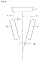
- the facing target sputtering method refers to a method of carrying out sputtering by placing two cathode targets to be opposed, and applying a magnetic field perpendicular to the target surfaces from one target toward the other target, unlike common magnetron sputtering methods. In this facing target sputtering method, the substrate 1 is placed perpendicular to the target on a side surface of the target.
- the buffer layer 4 is more easily obtained which has characteristics as represented by the formula (1) mentioned above.
- the angle ⁇ from at least one of the targets 6, 6' with respect to the imaginary central axis X is preferably set in the range of 5 to 15°, because the buffer layer 4 is further easily obtained which has characteristics as represented by the formula (1) mentioned above. It is to be noted the illustration of the rear electrode layer 2 and CIGS light absorbing layer 3 formed over the substrate 1 is omitted in FIG. 2 .
- Whether the obtained buffer layer 4 satisfies the formula (1) or not can be confirmed by, for example, measurement under the conditions of incident angle: 5° fixed and detector scan: 3°/min, with the use of a system from Bruker Corporation, XRD D8 DISCOVER with GADTS. It is to be noted that when the buffer layer 4 has multiple layers, at least a layer in contact with the CIGS light absorbing layer 3 only has to satisfy the formula (1). In addition, whether the buffer layer 4 satisfies the formulas (2) to (4) or not can be also confirmed by measurement under the same conditions as mentioned above.
- the transparent electrode layer 5 formed on the buffer layer 4 is preferably formed from a material that has a high transmission, and can be formed with the use of ITO, IZO, aluminum-containing zinc oxide (Al:ZnO), or the like.
- the thickness thereof preferably falls within the range of 50 to 300 nm.
- the light transmission of the transparent electrode layer 5 preferably exceeds 80%.
- this transparent electrode layer 5 can be formed by, for example, a sputtering method, a vapor deposition method, a metalorganic chemical vapor deposition (MOCVD) method, or the like.
- the buffer layer 4 can be continuously obtained by sputtering, and moreover, the conversion efficiency is improved because the CIGS light absorbing layer 3 has a chalcopyrite structure. Therefore, the CIGS light absorbing layer 3 can be made to a thin film, and the entire CIGS solar cell can be configured in the form of a thin film. In addition, because the CIGS solar cell can be configured in the form of a thin film, light of wavelengths which are not used can be transmitted with a high probability, and the cell can be expanded in use application and can increase subjects on which the cell can be disposed.
- the buffer layer 4 comprises a mixed crystal of a Group IIa metal and zinc oxide, and as described above, characteristics of this mixed crystal as shown by X-ray diffraction are adapted to satisfy the formula (1) mentioned above. Thus, the conversion efficiency is further improved. Furthermore, when the characteristics of the buffer layer 4 as shown by X-ray diffraction are adapted to satisfy the formulas (2) to (4), the buffer layer 4 is less likely to be cracked, and excellent in handling ability, even when a flexible substrate is used as the substrate 1.
- a rear electrode layer comprising Mo of 0.8 mm in thickness was formed at a sputtering rate of 60 m/min by using a magnetron sputtering system (from ULVAC, Inc., Model Number SH-450) with the use of argon for a discharge gas and with the use of a direct-current (DC) power source for providing a sputtering pressure of 1 Pa.
- a magnetron sputtering system from ULVAC, Inc., Model Number SH-450
- DC direct-current
- a CIGS light absorbing layer was formed on the rear electrode layer formed above. More specifically, while Ga, In, Cu, and Se were each placed as vapor deposition sources in a chamber of a vacuum deposition system, the substrate was heated up to 550°C at a rate of temperature increase of 550°C/h, with the degree of vacuum adjusted to 1 x 10 -4 Pa in the chamber. In this case, the CIGS light absorbing layer was formed on the rear electrode layer, in such a way that the vapor deposition sources were respectively heated so as to reach Ga (950°C), In (780°C), Cu (1100°C), and Se (140°C), for simultaneously evaporating these elements.
- a buffer layer was formed on the CIGS light absorbing layer formed above.
- the buffer layer was formed with the use of a facing target sputtering with the pair of targets 6, 6' shown in FIG. 2 arranged in a substantially V-shaped form (10° for each of the angles ⁇ from the targets 6, 6' with respect to the center line).
- a target of composition: Zn 0.85 Mg 0.15 O was used for a sputtering target, an edge 6'a of the target 6' was placed in a position 160 mm away from the surface of the substrate 1, and the temperature of the substrate 1 was set at 25°C.
- the composition analysis of the targets 6, 6' showed a mixture of about 3 at. % of Ca in Mg.
- Argon was used for the discharge gas during the sputtering, and the electric power and formation time were adjusted with a high-frequency RF power source, so as to achieve a power density of 0.7 W/cm 2 and a film thickness of 70 nm at a sputtering pressure of 0.3 Pa. It is to be noted that the edge 6'a of the target 6' refers to a part at the shortest distance from the substrate 1.
- a transparent electrode layer was formed on the buffer layer formed above.
- the transparent electrode layer was formed with the use of a magnetron sputtering system (from ULVAC, Inc., Model Number SH-450).
- a target of composition: ITO In 2 O 3 : 90 [at. %], SnO 2 : 10 [at. %] was used for the sputtering target.
- the results of measuring the conversion efficiency as described above have shown that the CIGS solar cells according to Examples 1 to 5 each have an excellent conversion efficiency with an average conversion efficiency of 3.3% or higher.
- the CIGS solar cell according to Comparative Examples 1 to 5 where characteristics of the buffer layers as shown by X-ray diffraction fail to satisfy the formula (1) have been shown to be each low in average conversion efficiency.
- the CIGS compound solar cell according to the present invention can be used in various fields, because the conversion efficiency is extremely high in spite of the thinness.
Landscapes
- Photovoltaic Devices (AREA)
- Life Sciences & Earth Sciences (AREA)
- Engineering & Computer Science (AREA)
- Sustainable Energy (AREA)
- Sustainable Development (AREA)
Applications Claiming Priority (3)
| Application Number | Priority Date | Filing Date | Title |
|---|---|---|---|
| JP2012040152 | 2012-02-27 | ||
| JP2012283071A JP6265362B2 (ja) | 2012-02-27 | 2012-12-26 | Cigs系化合物太陽電池 |
| PCT/JP2013/054720 WO2013129296A1 (ja) | 2012-02-27 | 2013-02-25 | Cigs系化合物太陽電池 |
Publications (3)
| Publication Number | Publication Date |
|---|---|
| EP2804221A1 true EP2804221A1 (de) | 2014-11-19 |
| EP2804221A4 EP2804221A4 (de) | 2015-10-28 |
| EP2804221B1 EP2804221B1 (de) | 2019-04-10 |
Family
ID=49082495
Family Applications (1)
| Application Number | Title | Priority Date | Filing Date |
|---|---|---|---|
| EP13755506.6A Active EP2804221B1 (de) | 2012-02-27 | 2013-02-25 | Solarzelle aus einer cigs-verbindung |
Country Status (7)
| Country | Link |
|---|---|
| US (1) | US9947808B2 (de) |
| EP (1) | EP2804221B1 (de) |
| JP (1) | JP6265362B2 (de) |
| KR (1) | KR101983422B1 (de) |
| CN (1) | CN104137272B (de) |
| TW (1) | TWI580060B (de) |
| WO (1) | WO2013129296A1 (de) |
Families Citing this family (5)
| Publication number | Priority date | Publication date | Assignee | Title |
|---|---|---|---|---|
| CN103474510B (zh) * | 2013-09-13 | 2016-03-09 | 厦门大学 | 一种铜铟镓硒薄膜太阳能电池的制作方法 |
| US10453978B2 (en) | 2015-03-12 | 2019-10-22 | International Business Machines Corporation | Single crystalline CZTSSe photovoltaic device |
| US9935214B2 (en) | 2015-10-12 | 2018-04-03 | International Business Machines Corporation | Liftoff process for exfoliation of thin film photovoltaic devices and back contact formation |
| JP2018074077A (ja) * | 2016-11-02 | 2018-05-10 | ソニー株式会社 | 撮像素子、固体撮像装置及び電子デバイス |
| US11728449B2 (en) | 2019-12-03 | 2023-08-15 | Applied Materials, Inc. | Copper, indium, gallium, selenium (CIGS) films with improved quantum efficiency |
Family Cites Families (14)
| Publication number | Priority date | Publication date | Assignee | Title |
|---|---|---|---|---|
| US6259016B1 (en) * | 1999-03-05 | 2001-07-10 | Matsushita Electric Industrial Co., Ltd. | Solar cell |
| JP3434259B2 (ja) * | 1999-03-05 | 2003-08-04 | 松下電器産業株式会社 | 太陽電池 |
| JP3837114B2 (ja) * | 1999-03-05 | 2006-10-25 | 松下電器産業株式会社 | 太陽電池 |
| JP4662616B2 (ja) | 2000-10-18 | 2011-03-30 | パナソニック株式会社 | 太陽電池 |
| JP4549570B2 (ja) | 2001-05-15 | 2010-09-22 | 昭和シェル石油株式会社 | ヘテロ接合薄膜太陽電池の製造方法 |
| JP2004363544A (ja) * | 2002-10-30 | 2004-12-24 | Canon Inc | 酸化亜鉛膜及びそれを用いた光起電力素子、酸化亜鉛膜の形成方法 |
| US20050189012A1 (en) | 2002-10-30 | 2005-09-01 | Canon Kabushiki Kaisha | Zinc oxide film, photovoltaic device making use of the same, and zinc oxide film formation process |
| JP2006269607A (ja) * | 2005-03-23 | 2006-10-05 | Canon Inc | 光起電力素子の製造方法 |
| US20100170566A1 (en) * | 2009-01-06 | 2010-07-08 | Arthur Don Harmala | Apparatus and method for manufacturing polymer solar cells |
| JP5003698B2 (ja) * | 2009-02-18 | 2012-08-15 | Tdk株式会社 | 太陽電池、及び太陽電池の製造方法 |
| JP4782855B2 (ja) * | 2009-03-12 | 2011-09-28 | 昭和シェル石油株式会社 | 化合物系薄膜太陽電池、及びその製造方法 |
| JP5478332B2 (ja) * | 2010-04-01 | 2014-04-23 | 日本プラスト株式会社 | エアバッグ装置 |
| JP5830882B2 (ja) * | 2010-04-08 | 2015-12-09 | 東ソー株式会社 | 酸化亜鉛系透明導電膜、その製造方法及びその用途 |
| JP5660004B2 (ja) | 2011-10-27 | 2015-01-28 | トヨタ自動車株式会社 | ZnMgO膜の製造方法 |
-
2012
- 2012-12-26 JP JP2012283071A patent/JP6265362B2/ja not_active Expired - Fee Related
-
2013
- 2013-02-25 TW TW102106515A patent/TWI580060B/zh not_active IP Right Cessation
- 2013-02-25 EP EP13755506.6A patent/EP2804221B1/de active Active
- 2013-02-25 KR KR1020147023188A patent/KR101983422B1/ko not_active Expired - Fee Related
- 2013-02-25 WO PCT/JP2013/054720 patent/WO2013129296A1/ja not_active Ceased
- 2013-02-25 US US14/376,761 patent/US9947808B2/en not_active Expired - Fee Related
- 2013-02-25 CN CN201380010209.XA patent/CN104137272B/zh not_active Expired - Fee Related
Also Published As
| Publication number | Publication date |
|---|---|
| US9947808B2 (en) | 2018-04-17 |
| TW201342635A (zh) | 2013-10-16 |
| JP2013211524A (ja) | 2013-10-10 |
| WO2013129296A1 (ja) | 2013-09-06 |
| CN104137272A (zh) | 2014-11-05 |
| KR20140129036A (ko) | 2014-11-06 |
| CN104137272B (zh) | 2016-01-20 |
| US20150027537A1 (en) | 2015-01-29 |
| EP2804221A4 (de) | 2015-10-28 |
| EP2804221B1 (de) | 2019-04-10 |
| TWI580060B (zh) | 2017-04-21 |
| KR101983422B1 (ko) | 2019-05-28 |
| JP6265362B2 (ja) | 2018-01-24 |
Similar Documents
| Publication | Publication Date | Title |
|---|---|---|
| JP2010192689A (ja) | 太陽電池、及び太陽電池の製造方法 | |
| EP2889919B1 (de) | Verbundsolarzelle und verfahren zu ihrer herstellung | |
| EP2804221B1 (de) | Solarzelle aus einer cigs-verbindung | |
| EP2808904A1 (de) | Verfahren zur herstellung einer zusammengesetzten solarzelle | |
| KR101081194B1 (ko) | 태양전지의 제조장치, 이를 이용한 태양전지의 제조방법 | |
| US9431558B2 (en) | CIGS type compound solar cell | |
| WO2011108033A1 (ja) | 化合物薄膜太陽電池及びその製造方法 | |
| KR20110048731A (ko) | 태양전지 및 이의 제조방법 | |
| JP2014225567A (ja) | Cigs系化合物太陽電池およびその製造方法 | |
| EP4318606A1 (de) | Photoelektrisches umwandlungselement und verfahren zur herstellung eines photoelektrischen umwandlungselements | |
| US20120067422A1 (en) | Photovoltaic device with a metal sulfide oxide window layer | |
| US20130137208A1 (en) | Method for manufacturing solar cell module | |
| JP2014017377A (ja) | 化合物太陽電池およびその製法 | |
| KR20150137161A (ko) | 태양 전지 및 이의 제조방법 |
Legal Events
| Date | Code | Title | Description |
|---|---|---|---|
| PUAI | Public reference made under article 153(3) epc to a published international application that has entered the european phase |
Free format text: ORIGINAL CODE: 0009012 |
|
| 17P | Request for examination filed |
Effective date: 20140813 |
|
| AK | Designated contracting states |
Kind code of ref document: A1 Designated state(s): AL AT BE BG CH CY CZ DE DK EE ES FI FR GB GR HR HU IE IS IT LI LT LU LV MC MK MT NL NO PL PT RO RS SE SI SK SM TR |
|
| DAX | Request for extension of the european patent (deleted) | ||
| RA4 | Supplementary search report drawn up and despatched (corrected) |
Effective date: 20150929 |
|
| RIC1 | Information provided on ipc code assigned before grant |
Ipc: H01L 31/032 20060101ALI20150923BHEP Ipc: H01L 31/0392 20060101ALI20150923BHEP Ipc: H01L 31/0328 20060101ALI20150923BHEP Ipc: H01L 31/0749 20120101AFI20150923BHEP |
|
| GRAP | Despatch of communication of intention to grant a patent |
Free format text: ORIGINAL CODE: EPIDOSNIGR1 |
|
| STAA | Information on the status of an ep patent application or granted ep patent |
Free format text: STATUS: GRANT OF PATENT IS INTENDED |
|
| INTG | Intention to grant announced |
Effective date: 20181221 |
|
| RIN1 | Information on inventor provided before grant (corrected) |
Inventor name: WATANABE, TAICHI Inventor name: KAWAMURA, KAZUNORI Inventor name: TERAJI, SEIKI Inventor name: NISHII, HIROTO |
|
| GRAS | Grant fee paid |
Free format text: ORIGINAL CODE: EPIDOSNIGR3 |
|
| GRAA | (expected) grant |
Free format text: ORIGINAL CODE: 0009210 |
|
| STAA | Information on the status of an ep patent application or granted ep patent |
Free format text: STATUS: THE PATENT HAS BEEN GRANTED |
|
| AK | Designated contracting states |
Kind code of ref document: B1 Designated state(s): AL AT BE BG CH CY CZ DE DK EE ES FI FR GB GR HR HU IE IS IT LI LT LU LV MC MK MT NL NO PL PT RO RS SE SI SK SM TR |
|
| REG | Reference to a national code |
Ref country code: GB Ref legal event code: FG4D |
|
| REG | Reference to a national code |
Ref country code: CH Ref legal event code: EP Ref country code: AT Ref legal event code: REF Ref document number: 1119863 Country of ref document: AT Kind code of ref document: T Effective date: 20190415 |
|
| REG | Reference to a national code |
Ref country code: IE Ref legal event code: FG4D |
|
| REG | Reference to a national code |
Ref country code: DE Ref legal event code: R096 Ref document number: 602013053721 Country of ref document: DE |
|
| REG | Reference to a national code |
Ref country code: NL Ref legal event code: MP Effective date: 20190410 |
|
| REG | Reference to a national code |
Ref country code: LT Ref legal event code: MG4D |
|
| REG | Reference to a national code |
Ref country code: AT Ref legal event code: MK05 Ref document number: 1119863 Country of ref document: AT Kind code of ref document: T Effective date: 20190410 |
|
| PG25 | Lapsed in a contracting state [announced via postgrant information from national office to epo] |
Ref country code: NL Free format text: LAPSE BECAUSE OF FAILURE TO SUBMIT A TRANSLATION OF THE DESCRIPTION OR TO PAY THE FEE WITHIN THE PRESCRIBED TIME-LIMIT Effective date: 20190410 |
|
| PG25 | Lapsed in a contracting state [announced via postgrant information from national office to epo] |
Ref country code: FI Free format text: LAPSE BECAUSE OF FAILURE TO SUBMIT A TRANSLATION OF THE DESCRIPTION OR TO PAY THE FEE WITHIN THE PRESCRIBED TIME-LIMIT Effective date: 20190410 Ref country code: LT Free format text: LAPSE BECAUSE OF FAILURE TO SUBMIT A TRANSLATION OF THE DESCRIPTION OR TO PAY THE FEE WITHIN THE PRESCRIBED TIME-LIMIT Effective date: 20190410 Ref country code: HR Free format text: LAPSE BECAUSE OF FAILURE TO SUBMIT A TRANSLATION OF THE DESCRIPTION OR TO PAY THE FEE WITHIN THE PRESCRIBED TIME-LIMIT Effective date: 20190410 Ref country code: PT Free format text: LAPSE BECAUSE OF FAILURE TO SUBMIT A TRANSLATION OF THE DESCRIPTION OR TO PAY THE FEE WITHIN THE PRESCRIBED TIME-LIMIT Effective date: 20190910 Ref country code: NO Free format text: LAPSE BECAUSE OF FAILURE TO SUBMIT A TRANSLATION OF THE DESCRIPTION OR TO PAY THE FEE WITHIN THE PRESCRIBED TIME-LIMIT Effective date: 20190710 Ref country code: SE Free format text: LAPSE BECAUSE OF FAILURE TO SUBMIT A TRANSLATION OF THE DESCRIPTION OR TO PAY THE FEE WITHIN THE PRESCRIBED TIME-LIMIT Effective date: 20190410 Ref country code: AL Free format text: LAPSE BECAUSE OF FAILURE TO SUBMIT A TRANSLATION OF THE DESCRIPTION OR TO PAY THE FEE WITHIN THE PRESCRIBED TIME-LIMIT Effective date: 20190410 |
|
| PG25 | Lapsed in a contracting state [announced via postgrant information from national office to epo] |
Ref country code: LV Free format text: LAPSE BECAUSE OF FAILURE TO SUBMIT A TRANSLATION OF THE DESCRIPTION OR TO PAY THE FEE WITHIN THE PRESCRIBED TIME-LIMIT Effective date: 20190410 Ref country code: GR Free format text: LAPSE BECAUSE OF FAILURE TO SUBMIT A TRANSLATION OF THE DESCRIPTION OR TO PAY THE FEE WITHIN THE PRESCRIBED TIME-LIMIT Effective date: 20190711 Ref country code: PL Free format text: LAPSE BECAUSE OF FAILURE TO SUBMIT A TRANSLATION OF THE DESCRIPTION OR TO PAY THE FEE WITHIN THE PRESCRIBED TIME-LIMIT Effective date: 20190410 Ref country code: RS Free format text: LAPSE BECAUSE OF FAILURE TO SUBMIT A TRANSLATION OF THE DESCRIPTION OR TO PAY THE FEE WITHIN THE PRESCRIBED TIME-LIMIT Effective date: 20190410 Ref country code: BG Free format text: LAPSE BECAUSE OF FAILURE TO SUBMIT A TRANSLATION OF THE DESCRIPTION OR TO PAY THE FEE WITHIN THE PRESCRIBED TIME-LIMIT Effective date: 20190710 |
|
| PG25 | Lapsed in a contracting state [announced via postgrant information from national office to epo] |
Ref country code: AT Free format text: LAPSE BECAUSE OF FAILURE TO SUBMIT A TRANSLATION OF THE DESCRIPTION OR TO PAY THE FEE WITHIN THE PRESCRIBED TIME-LIMIT Effective date: 20190410 Ref country code: IS Free format text: LAPSE BECAUSE OF FAILURE TO SUBMIT A TRANSLATION OF THE DESCRIPTION OR TO PAY THE FEE WITHIN THE PRESCRIBED TIME-LIMIT Effective date: 20190810 |
|
| REG | Reference to a national code |
Ref country code: DE Ref legal event code: R097 Ref document number: 602013053721 Country of ref document: DE |
|
| PG25 | Lapsed in a contracting state [announced via postgrant information from national office to epo] |
Ref country code: RO Free format text: LAPSE BECAUSE OF FAILURE TO SUBMIT A TRANSLATION OF THE DESCRIPTION OR TO PAY THE FEE WITHIN THE PRESCRIBED TIME-LIMIT Effective date: 20190410 Ref country code: CZ Free format text: LAPSE BECAUSE OF FAILURE TO SUBMIT A TRANSLATION OF THE DESCRIPTION OR TO PAY THE FEE WITHIN THE PRESCRIBED TIME-LIMIT Effective date: 20190410 Ref country code: SK Free format text: LAPSE BECAUSE OF FAILURE TO SUBMIT A TRANSLATION OF THE DESCRIPTION OR TO PAY THE FEE WITHIN THE PRESCRIBED TIME-LIMIT Effective date: 20190410 Ref country code: EE Free format text: LAPSE BECAUSE OF FAILURE TO SUBMIT A TRANSLATION OF THE DESCRIPTION OR TO PAY THE FEE WITHIN THE PRESCRIBED TIME-LIMIT Effective date: 20190410 Ref country code: DK Free format text: LAPSE BECAUSE OF FAILURE TO SUBMIT A TRANSLATION OF THE DESCRIPTION OR TO PAY THE FEE WITHIN THE PRESCRIBED TIME-LIMIT Effective date: 20190410 |
|
| PLBE | No opposition filed within time limit |
Free format text: ORIGINAL CODE: 0009261 |
|
| STAA | Information on the status of an ep patent application or granted ep patent |
Free format text: STATUS: NO OPPOSITION FILED WITHIN TIME LIMIT |
|
| PG25 | Lapsed in a contracting state [announced via postgrant information from national office to epo] |
Ref country code: IT Free format text: LAPSE BECAUSE OF FAILURE TO SUBMIT A TRANSLATION OF THE DESCRIPTION OR TO PAY THE FEE WITHIN THE PRESCRIBED TIME-LIMIT Effective date: 20190410 Ref country code: SM Free format text: LAPSE BECAUSE OF FAILURE TO SUBMIT A TRANSLATION OF THE DESCRIPTION OR TO PAY THE FEE WITHIN THE PRESCRIBED TIME-LIMIT Effective date: 20190410 |
|
| 26N | No opposition filed |
Effective date: 20200113 |
|
| PG25 | Lapsed in a contracting state [announced via postgrant information from national office to epo] |
Ref country code: TR Free format text: LAPSE BECAUSE OF FAILURE TO SUBMIT A TRANSLATION OF THE DESCRIPTION OR TO PAY THE FEE WITHIN THE PRESCRIBED TIME-LIMIT Effective date: 20190410 |
|
| PG25 | Lapsed in a contracting state [announced via postgrant information from national office to epo] |
Ref country code: SI Free format text: LAPSE BECAUSE OF FAILURE TO SUBMIT A TRANSLATION OF THE DESCRIPTION OR TO PAY THE FEE WITHIN THE PRESCRIBED TIME-LIMIT Effective date: 20190410 |
|
| REG | Reference to a national code |
Ref country code: DE Ref legal event code: R119 Ref document number: 602013053721 Country of ref document: DE |
|
| REG | Reference to a national code |
Ref country code: CH Ref legal event code: PL |
|
| GBPC | Gb: european patent ceased through non-payment of renewal fee |
Effective date: 20200225 |
|
| REG | Reference to a national code |
Ref country code: BE Ref legal event code: MM Effective date: 20200229 |
|
| PG25 | Lapsed in a contracting state [announced via postgrant information from national office to epo] |
Ref country code: ES Free format text: LAPSE BECAUSE OF FAILURE TO SUBMIT A TRANSLATION OF THE DESCRIPTION OR TO PAY THE FEE WITHIN THE PRESCRIBED TIME-LIMIT Effective date: 20190410 Ref country code: MC Free format text: LAPSE BECAUSE OF FAILURE TO SUBMIT A TRANSLATION OF THE DESCRIPTION OR TO PAY THE FEE WITHIN THE PRESCRIBED TIME-LIMIT Effective date: 20190410 Ref country code: LU Free format text: LAPSE BECAUSE OF NON-PAYMENT OF DUE FEES Effective date: 20200225 |
|
| PG25 | Lapsed in a contracting state [announced via postgrant information from national office to epo] |
Ref country code: LI Free format text: LAPSE BECAUSE OF NON-PAYMENT OF DUE FEES Effective date: 20200229 Ref country code: CH Free format text: LAPSE BECAUSE OF NON-PAYMENT OF DUE FEES Effective date: 20200229 |
|
| PG25 | Lapsed in a contracting state [announced via postgrant information from national office to epo] |
Ref country code: FR Free format text: LAPSE BECAUSE OF NON-PAYMENT OF DUE FEES Effective date: 20200229 Ref country code: IE Free format text: LAPSE BECAUSE OF NON-PAYMENT OF DUE FEES Effective date: 20200225 Ref country code: DE Free format text: LAPSE BECAUSE OF NON-PAYMENT OF DUE FEES Effective date: 20200901 Ref country code: GB Free format text: LAPSE BECAUSE OF NON-PAYMENT OF DUE FEES Effective date: 20200225 |
|
| PG25 | Lapsed in a contracting state [announced via postgrant information from national office to epo] |
Ref country code: BE Free format text: LAPSE BECAUSE OF NON-PAYMENT OF DUE FEES Effective date: 20200229 |
|
| PG25 | Lapsed in a contracting state [announced via postgrant information from national office to epo] |
Ref country code: MT Free format text: LAPSE BECAUSE OF FAILURE TO SUBMIT A TRANSLATION OF THE DESCRIPTION OR TO PAY THE FEE WITHIN THE PRESCRIBED TIME-LIMIT Effective date: 20190410 Ref country code: CY Free format text: LAPSE BECAUSE OF FAILURE TO SUBMIT A TRANSLATION OF THE DESCRIPTION OR TO PAY THE FEE WITHIN THE PRESCRIBED TIME-LIMIT Effective date: 20190410 |
|
| PG25 | Lapsed in a contracting state [announced via postgrant information from national office to epo] |
Ref country code: MK Free format text: LAPSE BECAUSE OF FAILURE TO SUBMIT A TRANSLATION OF THE DESCRIPTION OR TO PAY THE FEE WITHIN THE PRESCRIBED TIME-LIMIT Effective date: 20190410 |