EP2804457A1 - Dispositif de transport et de traitement de plaques conductrices - Google Patents
Dispositif de transport et de traitement de plaques conductrices Download PDFInfo
- Publication number
- EP2804457A1 EP2804457A1 EP13167690.0A EP13167690A EP2804457A1 EP 2804457 A1 EP2804457 A1 EP 2804457A1 EP 13167690 A EP13167690 A EP 13167690A EP 2804457 A1 EP2804457 A1 EP 2804457A1
- Authority
- EP
- European Patent Office
- Prior art keywords
- transport
- unit
- circuit boards
- printed circuit
- transport unit
- Prior art date
- Legal status (The legal status is an assumption and is not a legal conclusion. Google has not performed a legal analysis and makes no representation as to the accuracy of the status listed.)
- Granted
Links
- 238000012545 processing Methods 0.000 title claims abstract description 9
- 230000033001 locomotion Effects 0.000 claims description 25
- 238000012360 testing method Methods 0.000 claims description 20
- 238000007688 edging Methods 0.000 claims description 10
- 238000011109 contamination Methods 0.000 description 5
- 238000003860 storage Methods 0.000 description 5
- 238000013461 design Methods 0.000 description 4
- 230000005540 biological transmission Effects 0.000 description 3
- 239000002184 metal Substances 0.000 description 3
- 239000002245 particle Substances 0.000 description 2
- 238000012546 transfer Methods 0.000 description 2
- 238000004140 cleaning Methods 0.000 description 1
- 230000001419 dependent effect Effects 0.000 description 1
- 239000000428 dust Substances 0.000 description 1
- 230000014759 maintenance of location Effects 0.000 description 1
- 238000004519 manufacturing process Methods 0.000 description 1
- 239000000463 material Substances 0.000 description 1
- 238000000034 method Methods 0.000 description 1
- 238000012986 modification Methods 0.000 description 1
- 230000004048 modification Effects 0.000 description 1
- 239000000758 substrate Substances 0.000 description 1
- 238000013519 translation Methods 0.000 description 1
Images



Classifications
-
- B—PERFORMING OPERATIONS; TRANSPORTING
- B65—CONVEYING; PACKING; STORING; HANDLING THIN OR FILAMENTARY MATERIAL
- B65G—TRANSPORT OR STORAGE DEVICES, e.g. CONVEYORS FOR LOADING OR TIPPING, SHOP CONVEYOR SYSTEMS OR PNEUMATIC TUBE CONVEYORS
- B65G17/00—Conveyors having an endless traction element, e.g. a chain, transmitting movement to a continuous or substantially-continuous load-carrying surface or to a series of individual load-carriers; Endless-chain conveyors in which the chains form the load-carrying surface
- B65G17/12—Conveyors having an endless traction element, e.g. a chain, transmitting movement to a continuous or substantially-continuous load-carrying surface or to a series of individual load-carriers; Endless-chain conveyors in which the chains form the load-carrying surface comprising a series of individual load-carriers fixed, or normally fixed, relative to traction element
-
- H—ELECTRICITY
- H05—ELECTRIC TECHNIQUES NOT OTHERWISE PROVIDED FOR
- H05K—PRINTED CIRCUITS; CASINGS OR CONSTRUCTIONAL DETAILS OF ELECTRIC APPARATUS; MANUFACTURE OF ASSEMBLAGES OF ELECTRICAL COMPONENTS
- H05K13/00—Apparatus or processes specially adapted for manufacturing or adjusting assemblages of electric components
- H05K13/0061—Tools for holding the circuit boards during processing; handling transport of printed circuit boards
-
- G—PHYSICS
- G01—MEASURING; TESTING
- G01R—MEASURING ELECTRIC VARIABLES; MEASURING MAGNETIC VARIABLES
- G01R31/00—Arrangements for testing electric properties; Arrangements for locating electric faults; Arrangements for electrical testing characterised by what is being tested not provided for elsewhere
- G01R31/28—Testing of electronic circuits, e.g. by signal tracer
- G01R31/2851—Testing of integrated circuits [IC]
- G01R31/2893—Handling, conveying or loading, e.g. belts, boats, vacuum fingers
Definitions
- the invention relates to a device for transporting or transporting and processing printed circuit boards according to the preamble of claim 1.
- the object of the invention is in particular to provide a generic device with improved properties in terms of a compact design of the transport unit and in terms of a low load on printed circuit boards during transport.
- the object is achieved by the features of claim 1, while advantageous embodiments and modifications of the invention can be taken from the dependent claims.
- the invention is based on a device for transporting or for transporting and processing printed circuit boards, with at least one transport unit which is provided for a vertical conveyor and which has at least one transport belting means.
- the transport wrapping means have at least one transport bearing surface for supporting the printed circuit boards at least during transport.
- upright conveying should in this case in particular define a conveying of printed circuit boards along a transport direction of the transport unit, in which the element is vertically aligned during transport.
- vertical aligned is meant in particular an orientation of the circuit board, in which the main extension plane of the circuit board is aligned at least substantially perpendicular to a ground contact surface of the device.
- ground contact surface is intended here to define in particular a surface of the device by means of which the device can be placed on a substrate.
- the ground contact surface is preferably formed by a surface of a stand of the device, in particular a stand of a support frame unit of the device.
- substantially perpendicular is intended here to define, in particular, an orientation of a direction relative to a reference direction, the direction and the reference direction, in particular in one plane, including an angle of 90 ° and the angle a maximum deviation of, in particular, less than 8 °, advantageously less than 5 ° and particularly advantageously less than 2 °.
- a “transport belting means” is to be understood here as meaning, in particular, an element which at least partially wraps around a drive element, in particular a drive wheel, for transmission of drive forces and thus can be driven by the drive element.
- the Transportumschlingungsmittel can in this case be designed as a transport belt, as a conveyor belt, as a transport chain, etc.
- the term "transport bearing surface” is intended here to define in particular a surface of the transport wrapping means which is intended to bear against a transmission of transport forces directly to the printed circuit boards.
- the transport bearing surface can in this case be formed by a single, in particular flat, surface, which is aligned at least substantially transversely to a vertical axis of the transport unit.
- the transport bearing surface is composed of several partial surfaces which extend at least substantially transversely to each other, such as angled to each other, etc.
- a V-shaped transport bearing surface o. The like.
- the transport bearing surface extends at least substantially transversely to the vertical axis of the transport unit.
- substantially transversely is meant in particular an alignment of a direction and / or an axis relative to a reference direction and / or a reference axis, wherein the orientation of the direction and / or the axis at least different from an at least substantially parallel orientation to Reference direction and / or to the reference axis and in particular is skewed or perpendicular to the reference direction and / or to the reference axis.
- a “vertical axis” is to be understood here in particular an axis of the transport unit, which is aligned at least substantially perpendicular to the ground contact surface of the device.
- the vertical axis of the transport unit is designed as a vertical axis.
- the embodiment of the device according to the invention it is advantageously possible to enable a component-protecting delivery of the printed circuit boards. It can be advantageously made possible a low buckling load of the circuit board during transport of the circuit board by means of the device according to the invention.
- advantageous as a result of a vertical conveyor deflection of the circuit board during transport advantageous at least largely avoided.
- contamination of the printed circuit board, such as dust or chips as a result of contacting by means of contact needle elements, during transport can be advantageously avoided as a result of the edgewise conveyor.
- components can advantageously be saved for a transmission of transport forces.
- a compact transport unit or a compact device can be realized.
- the transport bearing surface extends at least substantially perpendicular to the vertical axis.
- the transport unit comprises at least one drive unit, which comprises at least one drive wheel, which is at least partially looped by the transport belt means.
- the drive unit may comprise support rollers, tension rollers, etc., which are provided to support and / or tension the transport belt means at least during a transport movement.
- the transport wrapping means is designed as a transport belt, which has a polygonal cross section.
- the transport belting means is formed endlessly or has a self-contained course.
- the transport belt comprises a rectangular or a quadrangular cross section.
- the transport belt has a 5-sided cross-section which forms a V-shaped receptacle on at least one side.
- the transport unit can have at least one support element which at least partially covers the transport belting means, which is designed as a transport belt, viewed along the vertical axis. It may be advantageous to achieve a guide surface in the region of the conveyor belt formed as a transport belt.
- the transport belt formed as a transport belt can be protected from contamination. It is conceivable that on the support element a Schmutzabweiserelement, such as a rubber lip is arranged, which can thus reduce contamination of the conveyor belt formed as a transport belt or largely avoided.
- a Schmutzabweiserelement such as a rubber lip is arranged, which can thus reduce contamination of the conveyor belt formed as a transport belt or largely avoided.
- the transport unit has at least one transport and / or guide element, which is designed as a guide rail.
- the transport wrapping means and the transport and / or guide element are preferably arranged spaced apart along the vertical axis.
- the printed circuit boards are preferably arranged between the transport belting means and the transport and / or guide element.
- the printed circuit boards are preferably located at least partially on the transport belting means and partly on the transport and / or guide element.
- the transport and / or guide element designed as a guide rail comprises at least one support and / or transport surface.
- the support and / or transport surface is provided to exert at least one support and / or holding force on the circuit boards whose main component of force extends at least substantially parallel to the vertical axis.
- substantially parallel is to be understood here as meaning, in particular, an alignment of a direction relative to a reference direction, in particular in a plane, wherein the direction relative to the reference direction is a deviation, in particular less than 8 °, advantageously less than 5 ° and particularly advantageously less than has 2 °.
- the term "main force component” is intended here in particular to define a component of a force, in particular a vectorial component of a force, which, in terms of percentage, defines the largest proportion with regard to an amount of the force.
- more than 40%, preferably more than 50% and particularly preferably more than 65% of the supporting and / or holding force act along at least one direction extending transversely to the vertical axis in at least one between the transport and / or guide element and the Transport wrapping arranged state of the circuit board on the circuit board, in particular during transport or during a holding of the circuit boards.
- the transport and / or guide element and the transport wrapping means are adjustable with respect to a position relative to each other.
- the transport and / or guide element and the Transportumschlingungsstoff can be adjusted continuously or in stages with respect to a position relative to each other.
- the device preferably comprises at least one locking unit, which is provided, the transport and / or guide element and the Transportumschlingungsstoff means of a positive and / or by means of a positive locking connection in a position to lock.
- the locking unit may in this case be formed integrally with a setting unit to adjust a position of the transport and / or guide element and the transport belt.
- the transport unit is preferably adjustable to various sizes and formats of printed circuit boards.
- the transport and / or guide element designed as a guide rail is mounted movably relative to the transport belting means along an axis of movement extending at least substantially parallel to the vertical axis.
- the transport and / or guide element formed as a guide rail is preferably arranged fixed to the frame on a support frame element of the transport unit.
- the support frame element per se is preferably movable relative to other components, in particular relative to a main frame, the transport unit stored.
- the transport and / or guide element designed as a guide rail is preferably mounted movably relative to the transporting means on a main frame of the transport unit by means of the support frame element of the transport unit.
- the transport and / or guide element designed as a guide rail comprises at least one guide groove in which the printed circuit boards are guided at least during transport.
- the support and / or transport surface of the guide and / or transport element designed as a guide rail rests directly against the printed circuit boards during guidance of the printed circuit boards during transport.
- the support and / or transport surface of the guide and / or transport element formed as a guide rail preferably lies directly on a surface of the printed circuit boards extending at least substantially perpendicular to a main extension plane of the printed circuit boards or on a transitional edge between the at least substantially perpendicular to a main extension plane Circuit board extending surface and an at least substantially parallel to the main extension plane extending surface of the circuit boards.
- a "main extension plane” is to be understood here in particular as a plane of the printed circuit boards in which the printed circuit boards have a maximum extent.
- the guide and / or transport element is preferably as an upper guide and / or transport element formed while the Transportumschlingungsmittel is preferably designed as a lower guide and / or transport element.
- at least the support and / or transport surface of the guide rail and / or transport element formed as a guide rail is formed from a friction-reducing material or provided with a friction-reducing layer.
- the support and / or transport surface is formed by a guide groove of the transport and / or guide element limiting surface of the guide rail designed as transport and / or guide element.
- the guide groove of the transport and / or guide element designed as a guide rail preferably has a U-shaped configuration.
- the transport and / or guide element designed as a guide rail has two support and / or transport surfaces which are mounted so as to be movable relative to one another.
- an adjustment of the support and / or transport surfaces to at least one dimension, in particular a thickness, of the printed circuit boards are made possible.
- the guide groove viewed along a direction extending at least substantially perpendicular to the vertical axis, has a receiving width which is less than 10 mm, preferably less than 8 mm and particularly preferably less than 6 mm.
- the groove viewed along a direction extending at least substantially perpendicular to the vertical axis, a receiving width, which has a value between 0.2 mm and 6 mm.
- a reliable guidance of the printed circuit boards during transport can advantageously be made possible. It can be advantageously prevented accidental tipping or falling out of the circuit boards from the transport and / or guide element.
- a precise guidance of the printed circuit boards during transport of the printed circuit boards can be made particularly advantageous.
- a stable arrangement of the printed circuit boards for transport and / or processing of the printed circuit boards are made possible.
- the device comprises at least one linear motion unit, which is provided to at least a portion of the transport unit to store translationally along a linear motion axis.
- the linear movement axis runs at least substantially perpendicular to the vertical axis.
- the linear movement axis preferably extends at least substantially perpendicular to the transport direction of the transport unit.
- the device comprises at least one pivoting unit which is provided to pivotally support at least a portion of the transport unit about a pivot axis.
- the pivot axis may in this case run at least substantially parallel and / or at least substantially perpendicular to the vertical axis.
- the device comprises at least one upright test unit, to which the printed circuit boards can be fed edgewise by means of the transport unit and by means of which the printed circuit boards can be tested in an upright arranged position.
- a direction of movement along which test elements of the upright test unit are movable is at least substantially perpendicular to the vertical axis.
- the device comprises at least one edging assembly, to which the printed circuit boards can be fed edgewise by means of the transport unit and by means of which the printed circuit boards can be fitted in an upright arranged position.
- a movement direction along which placement elements of the edging assembly unit are movable is at least substantially perpendicular to the vertical axis. It can be advantageously made possible a placement of printed circuit boards in a small space.
- a degree of contamination of printed circuit boards, which could affect an assembly are kept as low as possible, because of the upright orientation of the printed circuit boards advantageously an adhesion or a retention of dirt particles can be kept low in a region to be equipped.
- in combination with the support and / or transport surface of the transport and / or guide element can advantageously be achieved a stable positioning to a placement of the circuit boards.
- the device according to the invention should not be limited to the application and embodiment described above.
- the device according to the invention can have a number deviating from a number of individual elements, components and units mentioned herein.
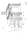
- FIG. 1 shows a device 10 for transport or for a transport and processing of printed circuit boards 12.
- the device 10 comprises various workstations in which the circuit boards 12 are for example populated, tested and / or cleaned.
- the device 10 is thus designed as a printed circuit board device.
- the individual workstations are formed in the device 10 as an edging assembly 44 and as edgewise test unit 42.
- the device 10 alternatively or additionally comprises further workstations, such as an upright cleaning unit, which is arranged along a transport direction 46 of the transport unit 14 between the edging assembly 44 and the edgewise test unit 42, etc.
- the printed circuit boards 12 are equipped with electronic components.
- the populated printed circuit boards 12 are supplied to a test of the edgewise test unit 42, in which the circuit boards 12 are tested for functionality.
- contact needle elements 52 (cf. FIG. 3 ) of the edgewise test unit 42 is brought into contact with the individual printed circuit boards 12 in order to allow testing of the printed circuit boards 12 for functionality.
- the contact needle elements 52 are moved along an at least substantially perpendicular to the vertical axis 20 of a transport unit 14 of the device 10 extending direction.
- a checking procedure takes place here, except for a vertical alignment of the edge-checking unit 42, at least substantially in a manner already known to a person skilled in the art.
- the edging assembly 44 and the edgewise test unit 42 are arranged one behind the other along the transport direction 46 of the transport unit 14.
- the upright assembly unit 44 and the upright test unit 42 have another arrangement that appears appropriate to a person skilled in the art relative to one another.
- the device 10 For feeding the printed circuit boards 12 to the individual work stations, the device 10 comprises at least the transport unit 14, which is provided for a vertical conveyor and which has at least one transport belt 16 (cf. Figures 2 and 7 ).
- the printed circuit boards 12 are thus transported vertically aligned by means of the transport unit 14 along the transport direction 46 of the transport unit 14.
- the transport belting means 16 has at least one transport bearing surface 18 for supporting the printed circuit boards 12 at least during transport.
- the transport bearing surface 18 extends at least substantially perpendicular to the vertical axis 20 of the transport unit 14.
- the vertical axis 20 is aligned at least substantially perpendicular to a ground contact surface 48 of the device 10.
- the ground contact surface 48 is formed by an area of at least one base 50 of the device 10.
- the transport belt 16 is formed as a transport belt having a polygonal cross section.
- the Transportumschlingungsmittel 16 may Longitudinal grooves to a guide and / or to a recording of the circuit boards 12 have or other, one of the skilled appearing reasonable leadership and / or receiving surface structures.
- the transport belt 16 formed as a transport belt has an at least substantially planar surface structure.
- the transport wrapping means 16 is arranged on a support frame element 68 of the transport unit 14.
- the support frame element 68 is in this case arranged in a stationary manner on a main frame element 70 of the transport unit 14. In this case, a main extension direction of the support frame element 68 extends at least substantially perpendicular to the vertical axis 20 of the transport unit 14.
- the device 10 has at least one drive unit 54 (cf. FIG. 2 ).
- the drive unit 54 is designed as an electric motor unit. However, it is also conceivable that the drive unit 54 has another, to those skilled appear appropriate design, such as an embodiment as a flow motor unit, etc.
- the drive unit 54 comprises at least one drive wheel 56 which is at least partially looped by the transport belt 16 (see. FIGS. 4 and 7 ).
- the drive wheel 56 is in this case rotatably mounted on the support frame member 68.
- at least one support element 72 of the transport unit 14 is arranged on the supporting frame element 68, which at least partially covers the transport belting means 16, designed as a transport belt, viewed along the vertical axis 20.
- the support member 72 also forms a lateral guide surface in the region of the conveyor belt formed as a transport belt 16, on which the circuit boards 12 can be guided during transport.
- the guide surface of the support element 72 extends in this case at least substantially parallel to the vertical axis 20 and to the transport direction 46.
- the transport unit 14 comprises along a total transport path a plurality of individual sections 30, 36 or partial transport units, each of which individually comprises a transport belt 16 by means of a drive unit 54 of the respective section 30, 36 of the transport unit 14 is drivable.
- the transport unit 14 For conveying the printed circuit boards 12 upright, the transport unit 14 comprises, in addition to the transport belting means 16, at least one transport and / or guide element 22 which is designed as a guide rail (cf. FIGS. 2 to 4 ). Show here the sections 30, 36 or partial transport units of the transport unit 14 each individually for themselves designed as a guide rail transport and / or guide element 22.
- the trained as a guide rail transport and / or guide member 22 is, viewed along the vertical axis 20, arranged relative to the transport belt means 16 spaced.
- the circuit boards 12 are arranged vertically aligned for transport between the Transportumschlingungsstoff 16 and formed as a guide rail transport and / or guide member 22.
- the printed circuit boards 12 each lie with one side on the transport belt 16 and in each case with a further side on the transport and / or guide element 22 designed as a guide rail.
- the transport and / or guide element 22 is arranged on a movably mounted further support frame element 58 of the transport unit 14.
- the further supporting frame element 58 is in this case mounted in a translationally movable manner on the main frame element 70 along a movement axis 24 running at least substantially parallel to the vertical axis 20.
- the device 10 comprises at least one vertical distance adjustment unit 60 for adjusting a distance between the transport belt 16 and the transport and / or guide element 22 formed as a guide rail along the vertical axis 20 (cf. FIG. 2 ).
- the vertical spacing adjustment unit 60 has a spindle element (not shown here in detail) and an operating element 62 acting on the spindle element.
- the operating element 62 is provided for rotationally driving the spindle element in a manner already known to a person skilled in the art in order to change or set a distance between the transport belting means 16 and the transport and / or guide element 22 formed as a guide rail along the vertical axis 20 ,
- the transport and / or guide element 22 designed as a guide rail is mounted movably relative to the transport belting means 16 along the movement axis 24 running at least substantially parallel to the vertical axis 20.
- the vertical spacing adjustment unit 60 comprises an electric, pneumatic and / or hydraulic linear drive unit, by means of which a distance between the transport belt means 16 and the transport and / or guide element 22 formed as a guide rail can be adjusted along the vertical axis 20 is.
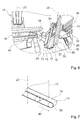
- the trained as a guide rail transport and / or guide member 22 further includes at least one guide groove 26 in which the circuit boards 12 are guided at least during transport (see. Figures 3 and 4 ).
- the guide groove 26 in this case has a U-shaped configuration. However, it is also conceivable that the guide groove 26 has another, a skilled person appear appropriate design, such as a V-shaped configuration, etc.
- formed as a guide rail transport and / or guide member 22 includes at least one support and / or Transport surface 64.
- the support and / or transport surface 64 is provided to exert at least one support and / or holding force on the circuit boards 12, the main force component extends at least substantially parallel to the vertical axis 20.
- the support and / or transport surface 64 is alternatively or additionally provided to exert at least one supporting and / or holding force on the printed circuit boards 12, the main force component extends at least substantially transversely to the vertical axis 20.
- the support and / or transport surface 64 of the transport and / or guide element 22 designed as a guide rail is formed by a surface of the transport and / or guide element 22 that defines the guide groove 26. Trained as a guide rail transport and / or guide element 22 is in this case formed of a plastic.
- the trained as a guide rail transport and / or guide member 22 is formed of a metal.
- the device 10 comprises at least one pivot unit 34, which is provided to at least a portion 36 of the transport unit 14 or at least a partial transport unit of the transport unit 14 to pivot about a pivot axis 38 to store (see. Figures 5 and 6 ).
- the pivot axis 38 of the pivot unit 34 in this case runs at least substantially parallel to the vertical axis 20 of the transport unit 14.
- the pivot axis 38 extends at least substantially transversely to the transport direction 46 of the transport unit 14.
- the device 10 comprises a further pivoting unit 66.
- the further pivoting unit 66 is provided for pivotally supporting at least the section 36 of the transporting unit 14 or at least the partial transporting unit of the transporting unit 14 about a further pivoting axis 40 (cf. Figures 5 and 6 ).
- the further pivot axis 40 extends in this case at least substantially perpendicular to the vertical axis 20 of the transport unit 14.
- the further pivot axis 40 extends at least substantially transversely to the transport direction 46 of the transport unit 14.
- the further pivot unit 66 is formed as a flip-pivot unit, which is provided for this purpose to pivot the printed circuit boards 12 from a vertical orientation to a horizontal orientation or vice versa.
- printed circuit boards 12 can be removed from a horizontal storage magazine of the device 10, which can be pivoted by means of the further pivot unit 66 in a vertical orientation to allow a transport of the circuit boards 12 by means of the transport unit 14 in a vertical orientation.
- a partial section of the transport unit 14 at which at least one transport belt 16 as described above, a transport and / or guide element 22 and a drive unit 54 are arranged as described above, pivoted relative to other portions of the transport unit 14 about the further pivot axis 40.
- the device 10 comprises at least one linear movement unit 28, which is provided to translate along at least one further section 30 of the transport unit 14 or at least one further partial transport unit of the transport unit 14 a linear motion axis 32 to store.
- the linear movement axis 32 extends in this case at least substantially perpendicular to the vertical axis 20 of the transport unit 14.
- the linear movement axis 32 extends at least substantially transversely and in particular perpendicular to the transport direction 46 of the transport unit 14.
- the linear movement unit 28 is thus designed as a parallel offset unit which is provided, at least the further section 30 of the transport unit 14 or at least the further part transport unit of the transport unit 14 in parallel relative z.
- a partial section of the transport unit 14 on which at least one transport belt 16 as described above becomes a transport and / or guide element 22 as described above and a drive unit 54 as described above, are moved in translation relative to other portions of the transport unit 14 along the linear movement axis 32.
- the printed circuit boards 12 can be fed upright by means of the transport unit 14 of the edging assembly 44.
- the printed circuit boards 12, as already described above can be equipped in an upright arranged position.
- the printed circuit boards 12 can be fed upright by means of the transport unit 14 of the upright test unit 42.
- the edgewise test unit 42 the printed circuit boards 12, as already described above, can be tested in an upright position.
- the apparatus 10 requires a small space in a production hall to realize transportation or transportation and processing of circuit boards 12.
Landscapes
- Engineering & Computer Science (AREA)
- Microelectronics & Electronic Packaging (AREA)
- Manufacturing & Machinery (AREA)
- Computer Hardware Design (AREA)
- General Engineering & Computer Science (AREA)
- Physics & Mathematics (AREA)
- General Physics & Mathematics (AREA)
- Mechanical Engineering (AREA)
- Framework For Endless Conveyors (AREA)
- Intermediate Stations On Conveyors (AREA)
- Structure Of Belt Conveyors (AREA)
- Supply And Installment Of Electrical Components (AREA)
Priority Applications (3)
| Application Number | Priority Date | Filing Date | Title |
|---|---|---|---|
| EP13167690.0A EP2804457B1 (fr) | 2013-05-14 | 2013-05-14 | Dispositif de transport et de traitement de plaques conductrices |
| US14/276,236 US20140339052A1 (en) | 2013-05-14 | 2014-05-13 | Apparatus for transporting, or for transporting and for processing, printed circuit boards |
| MX2014005829A MX2014005829A (es) | 2013-05-14 | 2014-05-14 | Dispositivo para un transporte o para un transporte y para una elaboracion de placas de circuito impreso. |
Applications Claiming Priority (1)
| Application Number | Priority Date | Filing Date | Title |
|---|---|---|---|
| EP13167690.0A EP2804457B1 (fr) | 2013-05-14 | 2013-05-14 | Dispositif de transport et de traitement de plaques conductrices |
Publications (2)
| Publication Number | Publication Date |
|---|---|
| EP2804457A1 true EP2804457A1 (fr) | 2014-11-19 |
| EP2804457B1 EP2804457B1 (fr) | 2016-04-20 |
Family
ID=48463759
Family Applications (1)
| Application Number | Title | Priority Date | Filing Date |
|---|---|---|---|
| EP13167690.0A Not-in-force EP2804457B1 (fr) | 2013-05-14 | 2013-05-14 | Dispositif de transport et de traitement de plaques conductrices |
Country Status (3)
| Country | Link |
|---|---|
| US (1) | US20140339052A1 (fr) |
| EP (1) | EP2804457B1 (fr) |
| MX (1) | MX2014005829A (fr) |
Cited By (1)
| Publication number | Priority date | Publication date | Assignee | Title |
|---|---|---|---|---|
| CN111470272A (zh) * | 2020-04-17 | 2020-07-31 | Oppo(重庆)智能科技有限公司 | 轨道系统与定位件 |
Citations (4)
| Publication number | Priority date | Publication date | Assignee | Title |
|---|---|---|---|---|
| US4957044A (en) * | 1989-06-19 | 1990-09-18 | Cronin John V | Double sided screener for printed circuit boards |
| WO1992021451A1 (fr) | 1991-06-05 | 1992-12-10 | Manufacturing Concepts & Technologies, Inc. | Installation pour le nettoyage de cartes a circuits imprimes |
| US6174382B1 (en) * | 1997-08-08 | 2001-01-16 | Intercontinental Chemical Corporation | Low pressure-high volume water washoff apparatus and process for cleaning and reclaiming screens |
| US20020133937A1 (en) * | 2000-04-27 | 2002-09-26 | Kazuhisa Mochida | System for mounting electronic device |
Family Cites Families (4)
| Publication number | Priority date | Publication date | Assignee | Title |
|---|---|---|---|---|
| DE4103849A1 (de) * | 1991-02-08 | 1992-08-13 | Licentia Gmbh | Vorrichtung zum ausschwenken eines ausschwenkmoduls aus einer foerderbandstrecke |
| EP0613730A3 (fr) * | 1993-03-01 | 1995-06-28 | Philips Nv | Dispositif de tri pourvu d'un champ d'unités de transport. |
| DE502004006191D1 (de) * | 2004-06-01 | 2008-03-27 | Applied Materials Gmbh & Co Kg | Messvorrichtung für die Messung des Transmissionsgrads einer Beschichtung |
| JP2006191039A (ja) * | 2005-01-05 | 2006-07-20 | Samsung Sdi Co Ltd | トレイ移送装置 |
-
2013
- 2013-05-14 EP EP13167690.0A patent/EP2804457B1/fr not_active Not-in-force
-
2014
- 2014-05-13 US US14/276,236 patent/US20140339052A1/en not_active Abandoned
- 2014-05-14 MX MX2014005829A patent/MX2014005829A/es unknown
Patent Citations (4)
| Publication number | Priority date | Publication date | Assignee | Title |
|---|---|---|---|---|
| US4957044A (en) * | 1989-06-19 | 1990-09-18 | Cronin John V | Double sided screener for printed circuit boards |
| WO1992021451A1 (fr) | 1991-06-05 | 1992-12-10 | Manufacturing Concepts & Technologies, Inc. | Installation pour le nettoyage de cartes a circuits imprimes |
| US6174382B1 (en) * | 1997-08-08 | 2001-01-16 | Intercontinental Chemical Corporation | Low pressure-high volume water washoff apparatus and process for cleaning and reclaiming screens |
| US20020133937A1 (en) * | 2000-04-27 | 2002-09-26 | Kazuhisa Mochida | System for mounting electronic device |
Cited By (2)
| Publication number | Priority date | Publication date | Assignee | Title |
|---|---|---|---|---|
| CN111470272A (zh) * | 2020-04-17 | 2020-07-31 | Oppo(重庆)智能科技有限公司 | 轨道系统与定位件 |
| CN111470272B (zh) * | 2020-04-17 | 2022-04-01 | Oppo(重庆)智能科技有限公司 | 轨道系统与定位件 |
Also Published As
| Publication number | Publication date |
|---|---|
| MX2014005829A (es) | 2014-11-24 |
| US20140339052A1 (en) | 2014-11-20 |
| EP2804457B1 (fr) | 2016-04-20 |
Similar Documents
| Publication | Publication Date | Title |
|---|---|---|
| DE2431244C2 (de) | Werkstück-Förderer | |
| DE3832845C1 (en) | Assembly station having a positioning and holding apparatus | |
| DE2419088B2 (de) | Vorrichtung zum Abstützen und Bewegen von Fördereinheiten | |
| DE102004034256B4 (de) | Vorrichtung zum Schneiden von Blech | |
| EP0258265A1 (fr) | Transporteur de pieces a usiner | |
| EP1979128A1 (fr) | Dispositif de manutention de pièces de type quelconque, en particulier pour le chargement et le dechargement lineaires de machines | |
| DE69201119T2 (de) | Lineare Fördervorrichtung mit freien Trägerplatten. | |
| DE19602297A1 (de) | Verfahren und Vorrichtung zum Vereinzeln von gedruckten Schaltungs-Platinen aus einem Stapel | |
| DE102008014831B4 (de) | Vorrichtung zum Puffern von Gegenständen | |
| DE3345920C2 (de) | Einrichtung zum automatischen Transport von Werkstücken | |
| DE3832865C1 (en) | Assembly station having a duplex conveyor | |
| EP2802441B1 (fr) | Installation de traitement du bois, et procédé permettant de faire fonctionner ladite installation de traitement du bois | |
| EP2804457B1 (fr) | Dispositif de transport et de traitement de plaques conductrices | |
| CH652377A5 (en) | Apparatus for transferring workpiece supports, workpieces or the like between transport tracks arranged transversely or parallel to each other | |
| AT514586B1 (de) | Vorrichtung zum Bearbeiten eines Endlosbandes mit einem Bandkörper aus Metall | |
| EP2535157A1 (fr) | Convoyeur à chaînes ou bandes | |
| DE10014199C1 (de) | Vorrichtung zum Transport von Leiterplatten | |
| DE102009013095B3 (de) | Sortierförderer zur Sortierung leichtgewichtiger, dünner und/oder flacher Sortiergüter | |
| DE3402497C2 (de) | Vorrichtung zum Kappen von Hölzern und zum anschließenden Bearbeiten der Holzabschnitte an den Seitenkanten | |
| DE102023113690B4 (de) | Vorrichtung mit Transportschiene und Verfahren zum Führen von Sägekettengliedern | |
| WO2002094691A2 (fr) | Dispositif de manipulation conçu pour deplacer des objets | |
| DE202012013216U1 (de) | Transporteinrichtung für Tiefziehverpackungsmaschine | |
| DE19931172C1 (de) | Vorrichtung zum Separieren von nebeneinander liegend geförderten, insbesondere aus Metall bestehenden Streifen | |
| CH667857A5 (de) | Vibrationsfoerdereinrichtung. | |
| DE3316981C2 (fr) |
Legal Events
| Date | Code | Title | Description |
|---|---|---|---|
| PUAI | Public reference made under article 153(3) epc to a published international application that has entered the european phase |
Free format text: ORIGINAL CODE: 0009012 |
|
| 17P | Request for examination filed |
Effective date: 20130522 |
|
| AK | Designated contracting states |
Kind code of ref document: A1 Designated state(s): AL AT BE BG CH CY CZ DE DK EE ES FI FR GB GR HR HU IE IS IT LI LT LU LV MC MK MT NL NO PL PT RO RS SE SI SK SM TR |
|
| AX | Request for extension of the european patent |
Extension state: BA ME |
|
| GRAP | Despatch of communication of intention to grant a patent |
Free format text: ORIGINAL CODE: EPIDOSNIGR1 |
|
| INTG | Intention to grant announced |
Effective date: 20151130 |
|
| GRAS | Grant fee paid |
Free format text: ORIGINAL CODE: EPIDOSNIGR3 |
|
| GRAA | (expected) grant |
Free format text: ORIGINAL CODE: 0009210 |
|
| AK | Designated contracting states |
Kind code of ref document: B1 Designated state(s): AL AT BE BG CH CY CZ DE DK EE ES FI FR GB GR HR HU IE IS IT LI LT LU LV MC MK MT NL NO PL PT RO RS SE SI SK SM TR |
|
| REG | Reference to a national code |
Ref country code: GB Ref legal event code: FG4D Free format text: NOT ENGLISH |
|
| REG | Reference to a national code |
Ref country code: CH Ref legal event code: NV Representative=s name: PATENTANWALTSKANZLEI DAUB, CH Ref country code: CH Ref legal event code: EP |
|
| REG | Reference to a national code |
Ref country code: AT Ref legal event code: REF Ref document number: 793666 Country of ref document: AT Kind code of ref document: T Effective date: 20160515 |
|
| REG | Reference to a national code |
Ref country code: IE Ref legal event code: FG4D Free format text: LANGUAGE OF EP DOCUMENT: GERMAN |
|
| REG | Reference to a national code |
Ref country code: FR Ref legal event code: PLFP Year of fee payment: 4 |
|
| REG | Reference to a national code |
Ref country code: DE Ref legal event code: R096 Ref document number: 502013002630 Country of ref document: DE |
|
| PGFP | Annual fee paid to national office [announced via postgrant information from national office to epo] |
Ref country code: DE Payment date: 20160531 Year of fee payment: 4 Ref country code: CH Payment date: 20160530 Year of fee payment: 4 |
|
| REG | Reference to a national code |
Ref country code: LT Ref legal event code: MG4D |
|
| PG25 | Lapsed in a contracting state [announced via postgrant information from national office to epo] |
Ref country code: BE Free format text: LAPSE BECAUSE OF NON-PAYMENT OF DUE FEES Effective date: 20160531 |
|
| PGFP | Annual fee paid to national office [announced via postgrant information from national office to epo] |
Ref country code: FR Payment date: 20160530 Year of fee payment: 4 |
|
| REG | Reference to a national code |
Ref country code: NL Ref legal event code: MP Effective date: 20160420 |
|
| REG | Reference to a national code |
Ref country code: CH Ref legal event code: PCAR Free format text: NEW ADDRESS: POSTFACH, 8058 ZUERICH-FLUGHAFEN (CH) |
|
| PG25 | Lapsed in a contracting state [announced via postgrant information from national office to epo] |
Ref country code: NO Free format text: LAPSE BECAUSE OF FAILURE TO SUBMIT A TRANSLATION OF THE DESCRIPTION OR TO PAY THE FEE WITHIN THE PRESCRIBED TIME-LIMIT Effective date: 20160720 Ref country code: PL Free format text: LAPSE BECAUSE OF FAILURE TO SUBMIT A TRANSLATION OF THE DESCRIPTION OR TO PAY THE FEE WITHIN THE PRESCRIBED TIME-LIMIT Effective date: 20160420 Ref country code: NL Free format text: LAPSE BECAUSE OF FAILURE TO SUBMIT A TRANSLATION OF THE DESCRIPTION OR TO PAY THE FEE WITHIN THE PRESCRIBED TIME-LIMIT Effective date: 20160420 Ref country code: FI Free format text: LAPSE BECAUSE OF FAILURE TO SUBMIT A TRANSLATION OF THE DESCRIPTION OR TO PAY THE FEE WITHIN THE PRESCRIBED TIME-LIMIT Effective date: 20160420 Ref country code: LT Free format text: LAPSE BECAUSE OF FAILURE TO SUBMIT A TRANSLATION OF THE DESCRIPTION OR TO PAY THE FEE WITHIN THE PRESCRIBED TIME-LIMIT Effective date: 20160420 |
|
| PG25 | Lapsed in a contracting state [announced via postgrant information from national office to epo] |
Ref country code: SE Free format text: LAPSE BECAUSE OF FAILURE TO SUBMIT A TRANSLATION OF THE DESCRIPTION OR TO PAY THE FEE WITHIN THE PRESCRIBED TIME-LIMIT Effective date: 20160420 Ref country code: HR Free format text: LAPSE BECAUSE OF FAILURE TO SUBMIT A TRANSLATION OF THE DESCRIPTION OR TO PAY THE FEE WITHIN THE PRESCRIBED TIME-LIMIT Effective date: 20160420 Ref country code: LV Free format text: LAPSE BECAUSE OF FAILURE TO SUBMIT A TRANSLATION OF THE DESCRIPTION OR TO PAY THE FEE WITHIN THE PRESCRIBED TIME-LIMIT Effective date: 20160420 Ref country code: GR Free format text: LAPSE BECAUSE OF FAILURE TO SUBMIT A TRANSLATION OF THE DESCRIPTION OR TO PAY THE FEE WITHIN THE PRESCRIBED TIME-LIMIT Effective date: 20160721 Ref country code: RS Free format text: LAPSE BECAUSE OF FAILURE TO SUBMIT A TRANSLATION OF THE DESCRIPTION OR TO PAY THE FEE WITHIN THE PRESCRIBED TIME-LIMIT Effective date: 20160420 Ref country code: PT Free format text: LAPSE BECAUSE OF FAILURE TO SUBMIT A TRANSLATION OF THE DESCRIPTION OR TO PAY THE FEE WITHIN THE PRESCRIBED TIME-LIMIT Effective date: 20160822 Ref country code: ES Free format text: LAPSE BECAUSE OF FAILURE TO SUBMIT A TRANSLATION OF THE DESCRIPTION OR TO PAY THE FEE WITHIN THE PRESCRIBED TIME-LIMIT Effective date: 20160420 |
|
| PG25 | Lapsed in a contracting state [announced via postgrant information from national office to epo] |
Ref country code: IT Free format text: LAPSE BECAUSE OF FAILURE TO SUBMIT A TRANSLATION OF THE DESCRIPTION OR TO PAY THE FEE WITHIN THE PRESCRIBED TIME-LIMIT Effective date: 20160420 |
|
| REG | Reference to a national code |
Ref country code: DE Ref legal event code: R097 Ref document number: 502013002630 Country of ref document: DE |
|
| PG25 | Lapsed in a contracting state [announced via postgrant information from national office to epo] |
Ref country code: CZ Free format text: LAPSE BECAUSE OF FAILURE TO SUBMIT A TRANSLATION OF THE DESCRIPTION OR TO PAY THE FEE WITHIN THE PRESCRIBED TIME-LIMIT Effective date: 20160420 Ref country code: RO Free format text: LAPSE BECAUSE OF FAILURE TO SUBMIT A TRANSLATION OF THE DESCRIPTION OR TO PAY THE FEE WITHIN THE PRESCRIBED TIME-LIMIT Effective date: 20160420 Ref country code: DK Free format text: LAPSE BECAUSE OF FAILURE TO SUBMIT A TRANSLATION OF THE DESCRIPTION OR TO PAY THE FEE WITHIN THE PRESCRIBED TIME-LIMIT Effective date: 20160420 Ref country code: SK Free format text: LAPSE BECAUSE OF FAILURE TO SUBMIT A TRANSLATION OF THE DESCRIPTION OR TO PAY THE FEE WITHIN THE PRESCRIBED TIME-LIMIT Effective date: 20160420 Ref country code: MC Free format text: LAPSE BECAUSE OF FAILURE TO SUBMIT A TRANSLATION OF THE DESCRIPTION OR TO PAY THE FEE WITHIN THE PRESCRIBED TIME-LIMIT Effective date: 20160420 Ref country code: EE Free format text: LAPSE BECAUSE OF FAILURE TO SUBMIT A TRANSLATION OF THE DESCRIPTION OR TO PAY THE FEE WITHIN THE PRESCRIBED TIME-LIMIT Effective date: 20160420 |
|
| REG | Reference to a national code |
Ref country code: IE Ref legal event code: MM4A |
|
| PLBE | No opposition filed within time limit |
Free format text: ORIGINAL CODE: 0009261 |
|
| STAA | Information on the status of an ep patent application or granted ep patent |
Free format text: STATUS: NO OPPOSITION FILED WITHIN TIME LIMIT |
|
| PG25 | Lapsed in a contracting state [announced via postgrant information from national office to epo] |
Ref country code: SM Free format text: LAPSE BECAUSE OF FAILURE TO SUBMIT A TRANSLATION OF THE DESCRIPTION OR TO PAY THE FEE WITHIN THE PRESCRIBED TIME-LIMIT Effective date: 20160420 |
|
| 26N | No opposition filed |
Effective date: 20170123 |
|
| PG25 | Lapsed in a contracting state [announced via postgrant information from national office to epo] |
Ref country code: SI Free format text: LAPSE BECAUSE OF FAILURE TO SUBMIT A TRANSLATION OF THE DESCRIPTION OR TO PAY THE FEE WITHIN THE PRESCRIBED TIME-LIMIT Effective date: 20160420 Ref country code: IE Free format text: LAPSE BECAUSE OF NON-PAYMENT OF DUE FEES Effective date: 20160514 |
|
| REG | Reference to a national code |
Ref country code: DE Ref legal event code: R119 Ref document number: 502013002630 Country of ref document: DE |
|
| REG | Reference to a national code |
Ref country code: CH Ref legal event code: PL |
|
| GBPC | Gb: european patent ceased through non-payment of renewal fee |
Effective date: 20170514 |
|
| PG25 | Lapsed in a contracting state [announced via postgrant information from national office to epo] |
Ref country code: LI Free format text: LAPSE BECAUSE OF NON-PAYMENT OF DUE FEES Effective date: 20170531 Ref country code: CH Free format text: LAPSE BECAUSE OF NON-PAYMENT OF DUE FEES Effective date: 20170531 |
|
| REG | Reference to a national code |
Ref country code: FR Ref legal event code: ST Effective date: 20180131 |
|
| PG25 | Lapsed in a contracting state [announced via postgrant information from national office to epo] |
Ref country code: GB Free format text: LAPSE BECAUSE OF NON-PAYMENT OF DUE FEES Effective date: 20170514 Ref country code: DE Free format text: LAPSE BECAUSE OF NON-PAYMENT OF DUE FEES Effective date: 20171201 |
|
| PG25 | Lapsed in a contracting state [announced via postgrant information from national office to epo] |
Ref country code: HU Free format text: LAPSE BECAUSE OF FAILURE TO SUBMIT A TRANSLATION OF THE DESCRIPTION OR TO PAY THE FEE WITHIN THE PRESCRIBED TIME-LIMIT; INVALID AB INITIO Effective date: 20130514 Ref country code: FR Free format text: LAPSE BECAUSE OF NON-PAYMENT OF DUE FEES Effective date: 20170531 |
|
| PG25 | Lapsed in a contracting state [announced via postgrant information from national office to epo] |
Ref country code: MK Free format text: LAPSE BECAUSE OF FAILURE TO SUBMIT A TRANSLATION OF THE DESCRIPTION OR TO PAY THE FEE WITHIN THE PRESCRIBED TIME-LIMIT Effective date: 20160420 Ref country code: IS Free format text: LAPSE BECAUSE OF FAILURE TO SUBMIT A TRANSLATION OF THE DESCRIPTION OR TO PAY THE FEE WITHIN THE PRESCRIBED TIME-LIMIT Effective date: 20160420 Ref country code: CY Free format text: LAPSE BECAUSE OF FAILURE TO SUBMIT A TRANSLATION OF THE DESCRIPTION OR TO PAY THE FEE WITHIN THE PRESCRIBED TIME-LIMIT Effective date: 20160420 Ref country code: LU Free format text: LAPSE BECAUSE OF NON-PAYMENT OF DUE FEES Effective date: 20160514 Ref country code: MT Free format text: LAPSE BECAUSE OF FAILURE TO SUBMIT A TRANSLATION OF THE DESCRIPTION OR TO PAY THE FEE WITHIN THE PRESCRIBED TIME-LIMIT Effective date: 20160420 |
|
| PG25 | Lapsed in a contracting state [announced via postgrant information from national office to epo] |
Ref country code: BG Free format text: LAPSE BECAUSE OF FAILURE TO SUBMIT A TRANSLATION OF THE DESCRIPTION OR TO PAY THE FEE WITHIN THE PRESCRIBED TIME-LIMIT Effective date: 20160420 |
|
| PG25 | Lapsed in a contracting state [announced via postgrant information from national office to epo] |
Ref country code: TR Free format text: LAPSE BECAUSE OF FAILURE TO SUBMIT A TRANSLATION OF THE DESCRIPTION OR TO PAY THE FEE WITHIN THE PRESCRIBED TIME-LIMIT Effective date: 20160420 Ref country code: AL Free format text: LAPSE BECAUSE OF FAILURE TO SUBMIT A TRANSLATION OF THE DESCRIPTION OR TO PAY THE FEE WITHIN THE PRESCRIBED TIME-LIMIT Effective date: 20160420 |
|
| REG | Reference to a national code |
Ref country code: AT Ref legal event code: MM01 Ref document number: 793666 Country of ref document: AT Kind code of ref document: T Effective date: 20180514 |
|
| PG25 | Lapsed in a contracting state [announced via postgrant information from national office to epo] |
Ref country code: AT Free format text: LAPSE BECAUSE OF NON-PAYMENT OF DUE FEES Effective date: 20180514 |