EP2804925B1 - Geformter nanopartikelphosphor für lichtemittierende anwendungen - Google Patents
Geformter nanopartikelphosphor für lichtemittierende anwendungen Download PDFInfo
- Publication number
- EP2804925B1 EP2804925B1 EP13714996.9A EP13714996A EP2804925B1 EP 2804925 B1 EP2804925 B1 EP 2804925B1 EP 13714996 A EP13714996 A EP 13714996A EP 2804925 B1 EP2804925 B1 EP 2804925B1
- Authority
- EP
- European Patent Office
- Prior art keywords
- matrix material
- nanoparticle phosphor
- molded
- coating
- nanoparticles
- Prior art date
- Legal status (The legal status is an assumption and is not a legal conclusion. Google has not performed a legal analysis and makes no representation as to the accuracy of the status listed.)
- Active
Links
Images

Classifications
-
- H—ELECTRICITY
- H10—SEMICONDUCTOR DEVICES; ELECTRIC SOLID-STATE DEVICES NOT OTHERWISE PROVIDED FOR
- H10H—INORGANIC LIGHT-EMITTING SEMICONDUCTOR DEVICES HAVING POTENTIAL BARRIERS
- H10H20/00—Individual inorganic light-emitting semiconductor devices having potential barriers, e.g. light-emitting diodes [LED]
- H10H20/80—Constructional details
- H10H20/85—Packages
- H10H20/8506—Containers
-
- B—PERFORMING OPERATIONS; TRANSPORTING
- B82—NANOTECHNOLOGY
- B82Y—SPECIFIC USES OR APPLICATIONS OF NANOSTRUCTURES; MEASUREMENT OR ANALYSIS OF NANOSTRUCTURES; MANUFACTURE OR TREATMENT OF NANOSTRUCTURES
- B82Y40/00—Manufacture or treatment of nanostructures
-
- C—CHEMISTRY; METALLURGY
- C09—DYES; PAINTS; POLISHES; NATURAL RESINS; ADHESIVES; COMPOSITIONS NOT OTHERWISE PROVIDED FOR; APPLICATIONS OF MATERIALS NOT OTHERWISE PROVIDED FOR
- C09D—COATING COMPOSITIONS, e.g. PAINTS, VARNISHES OR LACQUERS; FILLING PASTES; CHEMICAL PAINT OR INK REMOVERS; INKS; CORRECTING FLUIDS; WOODSTAINS; PASTES OR SOLIDS FOR COLOURING OR PRINTING; USE OF MATERIALS THEREFOR
- C09D165/00—Coating compositions based on macromolecular compounds obtained by reactions forming a carbon-to-carbon link in the main chain; Coating compositions based on derivatives of such polymers
-
- C—CHEMISTRY; METALLURGY
- C09—DYES; PAINTS; POLISHES; NATURAL RESINS; ADHESIVES; COMPOSITIONS NOT OTHERWISE PROVIDED FOR; APPLICATIONS OF MATERIALS NOT OTHERWISE PROVIDED FOR
- C09K—MATERIALS FOR MISCELLANEOUS APPLICATIONS, NOT PROVIDED FOR ELSEWHERE
- C09K11/00—Luminescent materials, e.g. electroluminescent or chemiluminescent
- C09K11/02—Use of particular materials as binders, particle coatings or suspension media therefor
-
- C—CHEMISTRY; METALLURGY
- C09—DYES; PAINTS; POLISHES; NATURAL RESINS; ADHESIVES; COMPOSITIONS NOT OTHERWISE PROVIDED FOR; APPLICATIONS OF MATERIALS NOT OTHERWISE PROVIDED FOR
- C09K—MATERIALS FOR MISCELLANEOUS APPLICATIONS, NOT PROVIDED FOR ELSEWHERE
- C09K11/00—Luminescent materials, e.g. electroluminescent or chemiluminescent
- C09K11/08—Luminescent materials, e.g. electroluminescent or chemiluminescent containing inorganic luminescent materials
-
- C—CHEMISTRY; METALLURGY
- C09—DYES; PAINTS; POLISHES; NATURAL RESINS; ADHESIVES; COMPOSITIONS NOT OTHERWISE PROVIDED FOR; APPLICATIONS OF MATERIALS NOT OTHERWISE PROVIDED FOR
- C09K—MATERIALS FOR MISCELLANEOUS APPLICATIONS, NOT PROVIDED FOR ELSEWHERE
- C09K11/00—Luminescent materials, e.g. electroluminescent or chemiluminescent
- C09K11/08—Luminescent materials, e.g. electroluminescent or chemiluminescent containing inorganic luminescent materials
- C09K11/56—Luminescent materials, e.g. electroluminescent or chemiluminescent containing inorganic luminescent materials containing sulfur
-
- C—CHEMISTRY; METALLURGY
- C09—DYES; PAINTS; POLISHES; NATURAL RESINS; ADHESIVES; COMPOSITIONS NOT OTHERWISE PROVIDED FOR; APPLICATIONS OF MATERIALS NOT OTHERWISE PROVIDED FOR
- C09K—MATERIALS FOR MISCELLANEOUS APPLICATIONS, NOT PROVIDED FOR ELSEWHERE
- C09K11/00—Luminescent materials, e.g. electroluminescent or chemiluminescent
- C09K11/08—Luminescent materials, e.g. electroluminescent or chemiluminescent containing inorganic luminescent materials
- C09K11/70—Luminescent materials, e.g. electroluminescent or chemiluminescent containing inorganic luminescent materials containing phosphorus
-
- H—ELECTRICITY
- H05—ELECTRIC TECHNIQUES NOT OTHERWISE PROVIDED FOR
- H05B—ELECTRIC HEATING; ELECTRIC LIGHT SOURCES NOT OTHERWISE PROVIDED FOR; CIRCUIT ARRANGEMENTS FOR ELECTRIC LIGHT SOURCES, IN GENERAL
- H05B33/00—Electroluminescent light sources
- H05B33/12—Light sources with substantially two-dimensional [2D] radiating surfaces
- H05B33/14—Light sources with substantially two-dimensional [2D] radiating surfaces characterised by the chemical or physical composition or the arrangement of the electroluminescent material, or by the simultaneous addition of the electroluminescent material in or onto the light source
-
- H—ELECTRICITY
- H10—SEMICONDUCTOR DEVICES; ELECTRIC SOLID-STATE DEVICES NOT OTHERWISE PROVIDED FOR
- H10H—INORGANIC LIGHT-EMITTING SEMICONDUCTOR DEVICES HAVING POTENTIAL BARRIERS
- H10H20/00—Individual inorganic light-emitting semiconductor devices having potential barriers, e.g. light-emitting diodes [LED]
- H10H20/80—Constructional details
- H10H20/85—Packages
- H10H20/851—Wavelength conversion means
-
- H—ELECTRICITY
- H10—SEMICONDUCTOR DEVICES; ELECTRIC SOLID-STATE DEVICES NOT OTHERWISE PROVIDED FOR
- H10H—INORGANIC LIGHT-EMITTING SEMICONDUCTOR DEVICES HAVING POTENTIAL BARRIERS
- H10H20/00—Individual inorganic light-emitting semiconductor devices having potential barriers, e.g. light-emitting diodes [LED]
- H10H20/80—Constructional details
- H10H20/85—Packages
- H10H20/851—Wavelength conversion means
- H10H20/8511—Wavelength conversion means characterised by their material, e.g. binder
- H10H20/8512—Wavelength conversion materials
-
- H—ELECTRICITY
- H10—SEMICONDUCTOR DEVICES; ELECTRIC SOLID-STATE DEVICES NOT OTHERWISE PROVIDED FOR
- H10H—INORGANIC LIGHT-EMITTING SEMICONDUCTOR DEVICES HAVING POTENTIAL BARRIERS
- H10H20/00—Individual inorganic light-emitting semiconductor devices having potential barriers, e.g. light-emitting diodes [LED]
- H10H20/80—Constructional details
- H10H20/85—Packages
- H10H20/851—Wavelength conversion means
- H10H20/8514—Wavelength conversion means characterised by their shape, e.g. plate or foil
-
- C—CHEMISTRY; METALLURGY
- C08—ORGANIC MACROMOLECULAR COMPOUNDS; THEIR PREPARATION OR CHEMICAL WORKING-UP; COMPOSITIONS BASED THEREON
- C08G—MACROMOLECULAR COMPOUNDS OBTAINED OTHERWISE THAN BY REACTIONS ONLY INVOLVING UNSATURATED CARBON-TO-CARBON BONDS
- C08G2261/00—Macromolecular compounds obtained by reactions forming a carbon-to-carbon link in the main chain of the macromolecule
- C08G2261/30—Monomer units or repeat units incorporating structural elements in the main chain
- C08G2261/34—Monomer units or repeat units incorporating structural elements in the main chain incorporating partially-aromatic structural elements in the main chain
- C08G2261/342—Monomer units or repeat units incorporating structural elements in the main chain incorporating partially-aromatic structural elements in the main chain containing only carbon atoms
- C08G2261/3424—Monomer units or repeat units incorporating structural elements in the main chain incorporating partially-aromatic structural elements in the main chain containing only carbon atoms non-conjugated, e.g. paracyclophanes or xylenes
-
- C—CHEMISTRY; METALLURGY
- C08—ORGANIC MACROMOLECULAR COMPOUNDS; THEIR PREPARATION OR CHEMICAL WORKING-UP; COMPOSITIONS BASED THEREON
- C08G—MACROMOLECULAR COMPOUNDS OBTAINED OTHERWISE THAN BY REACTIONS ONLY INVOLVING UNSATURATED CARBON-TO-CARBON BONDS
- C08G2261/00—Macromolecular compounds obtained by reactions forming a carbon-to-carbon link in the main chain of the macromolecule
- C08G2261/30—Monomer units or repeat units incorporating structural elements in the main chain
- C08G2261/34—Monomer units or repeat units incorporating structural elements in the main chain incorporating partially-aromatic structural elements in the main chain
- C08G2261/344—Monomer units or repeat units incorporating structural elements in the main chain incorporating partially-aromatic structural elements in the main chain containing heteroatoms
- C08G2261/3442—Polyetherketones
-
- C—CHEMISTRY; METALLURGY
- C08—ORGANIC MACROMOLECULAR COMPOUNDS; THEIR PREPARATION OR CHEMICAL WORKING-UP; COMPOSITIONS BASED THEREON
- C08G—MACROMOLECULAR COMPOUNDS OBTAINED OTHERWISE THAN BY REACTIONS ONLY INVOLVING UNSATURATED CARBON-TO-CARBON BONDS
- C08G2261/00—Macromolecular compounds obtained by reactions forming a carbon-to-carbon link in the main chain of the macromolecule
- C08G2261/90—Applications
- C08G2261/95—Use in organic luminescent diodes
-
- C—CHEMISTRY; METALLURGY
- C09—DYES; PAINTS; POLISHES; NATURAL RESINS; ADHESIVES; COMPOSITIONS NOT OTHERWISE PROVIDED FOR; APPLICATIONS OF MATERIALS NOT OTHERWISE PROVIDED FOR
- C09D—COATING COMPOSITIONS, e.g. PAINTS, VARNISHES OR LACQUERS; FILLING PASTES; CHEMICAL PAINT OR INK REMOVERS; INKS; CORRECTING FLUIDS; WOODSTAINS; PASTES OR SOLIDS FOR COLOURING OR PRINTING; USE OF MATERIALS THEREFOR
- C09D4/00—Coating compositions, e.g. paints, varnishes or lacquers, based on organic non-macromolecular compounds having at least one polymerisable carbon-to-carbon unsaturated bond ; Coating compositions, based on monomers of macromolecular compounds of groups C09D183/00 - C09D183/16
-
- H—ELECTRICITY
- H10—SEMICONDUCTOR DEVICES; ELECTRIC SOLID-STATE DEVICES NOT OTHERWISE PROVIDED FOR
- H10H—INORGANIC LIGHT-EMITTING SEMICONDUCTOR DEVICES HAVING POTENTIAL BARRIERS
- H10H20/00—Individual inorganic light-emitting semiconductor devices having potential barriers, e.g. light-emitting diodes [LED]
- H10H20/01—Manufacture or treatment
- H10H20/036—Manufacture or treatment of packages
- H10H20/0361—Manufacture or treatment of packages of wavelength conversion means
-
- H—ELECTRICITY
- H10—SEMICONDUCTOR DEVICES; ELECTRIC SOLID-STATE DEVICES NOT OTHERWISE PROVIDED FOR
- H10W—GENERIC PACKAGES, INTERCONNECTIONS, CONNECTORS OR OTHER CONSTRUCTIONAL DETAILS OF DEVICES COVERED BY CLASS H10
- H10W90/00—Package configurations
- H10W90/701—Package configurations characterised by the relative positions of pads or connectors relative to package parts
- H10W90/751—Package configurations characterised by the relative positions of pads or connectors relative to package parts of bond wires
- H10W90/754—Package configurations characterised by the relative positions of pads or connectors relative to package parts of bond wires between a chip and a stacked insulating package substrate, interposer or RDL
-
- Y—GENERAL TAGGING OF NEW TECHNOLOGICAL DEVELOPMENTS; GENERAL TAGGING OF CROSS-SECTIONAL TECHNOLOGIES SPANNING OVER SEVERAL SECTIONS OF THE IPC; TECHNICAL SUBJECTS COVERED BY FORMER USPC CROSS-REFERENCE ART COLLECTIONS [XRACs] AND DIGESTS
- Y10—TECHNICAL SUBJECTS COVERED BY FORMER USPC
- Y10S—TECHNICAL SUBJECTS COVERED BY FORMER USPC CROSS-REFERENCE ART COLLECTIONS [XRACs] AND DIGESTS
- Y10S977/00—Nanotechnology
- Y10S977/70—Nanostructure
- Y10S977/773—Nanoparticle, i.e. structure having three dimensions of 100 nm or less
Definitions
- QDs quantum dots
- nanoparticles Semiconductor nanoparticles are gaining substantial interest due to their applicability for commercial applications as diverse as biological labeling, solar cells, catalysis, biological imaging, and light-emitting diodes.
- LEDs are becoming increasingly important, in for example, automobile lighting, traffic signals, general lighting, and liquid crystal display (LCD) backlighting and display screens.
- Nanoparticle-based light-emitting devices have been made by embedding semiconductor nanoparticles in an optically clear (or sufficiently transparent) LED encapsulation medium, typically a silicone or an acrylate, which is then placed on top of a solid-state LED. The nanoparticles, excited by the primary light of the solid-state LED, emit secondary light, the color of which is characteristic of the particular type and size of the nanoparticles.
- an optically clear (or sufficiently transparent) LED encapsulation medium typically a silicone or an acrylate
- the nanoparticles will absorb a portion of the blue light and emit red light. A portion of the solid-state LED emission is thereby "down-converted" and the device provides light that is a mixture of blue and red.
- semiconductor nanoparticles potentially has significant advantages over the use of the more conventional phosphors.
- semiconductor nanoparticles provide the ability to tune the emission wavelength of a LED.
- oxygen can still migrate through the encapsulant to the surfaces of the nanoparticles, which can lead to photo-oxidation and, as a result, a drop in quantum yield (QY).
- quantum dot-based light-emitting devices In view of the significant potential for the application of quantum dots across such a wide range of applications, including but not limited to, quantum dot-based light-emitting devices, there is a strong need to develop methods to increase the stability of quantum dots so as to make them brighter, more long-lived and/or less sensitive to various types of processing conditions. There remain significant challenges to the development of quantum dot-based materials and methods for fabricating quantum dot-based devices, such as light-emitting devices, on an economically viable scale and which would provide sufficiently high levels of performance to satisfy consumer demand.
- a molded nanoparticle phosphor for light emitting applications is fabricated by converting a suspension of nanoparticles in a matrix material precursor into a molded nanoparticle phosphor comprising a matrix material and the nanoparticles.
- the matrix material can be any material in which the nanoparticles are dispersible and which is moldable.
- the matrix material can be a polymeric material. If the matrix material is a polymeric material, then the matrix material precursor can be a formulation of the appropriate monomers.
- the matrix material precursor may also contain catalysts, crosslinking agents, initiators, and the like.
- the molded nanoparticle phosphor can be formed from the matrix material precursor/nanoparticle suspension using any molding technique, such as polymerization molding, contact molding, extrusion molding, injection molding, for example.
- the molded nanoparticle phosphor can be coated with a gas barrier material, for example, a polymer, metal oxide, metal nitride or a glass.
- the coating can be applied to the molded nanoparticle phosphor by any coating technique, such as atomic layer deposition, evaporation coating, spray coating, or brush coating.
- the barrier-coated molded nanoparticle phosphor can be utilized in a light-emitting device, such as an LED.
- the phosphor can be incorporated into the packaging of a standard solid state LED and used to down-convert a portion of the emission of the solid state LED emitter.
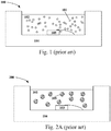
- FIG. 1 illustrates a prior art nanoparticle-based light-emitting device 100 as described in the background.
- the light-emitting device 100 has semiconductor nanoparticles 101 in an optically clear (or sufficiently transparent) LED encapsulation medium 102, typically a silicone or an acrylate, which is then placed on top of a solid-state LED 103.
- the encapsulation medium is contained within a package 104.
- QY quantum yield
- FIG. 2A illustrates a prior art nanoparticle-based light emitting device 200 that addresses the problem of photo-oxidation due to oxygen that migrates into the encapsulant 202.
- the nanoparticles 201 are incorporated into microbeads 205, which are suspended in the LED encapsulant 202. Bead 205 is illustrated in more detail in FIG. 2B .
- Nanoparticles 201 are incorporated into a primary matrix material 206.
- the primary matrix material is preferably an optically transparent medium, i.e., a medium through which light may pass, and which may be, but does not have to be substantially optically clear.
- the primary matrix may be a resin, polymer, monolith, glass, sol gel, epoxy, silicone, (meth)acrylate or the like, or may include silica.
- primary matrix materials include acrylate polymers (e.g., polymethyl(meth)acrylate, polybutylmethacrylate, polyoctylmethacrylate, alkylcyanoacryaltes, polyethyleneglycol dimethacrylate, polyvinylacetate etc), epoxides (e.g., EPOTEK 301 A+B Thermal curing epoxy, EPOTEK OG112-4 single pot UV curing epoxy, or EX0135A and B Thermal curing epoxy), polyamides, polyimides, polyesters, polycarbonates, polythioethers, polyacrylonitryls, polydienes, polystyrene polybutadiene copolymers (Kratons), pyrelenes, poly-para-xylylene (parylenes), silica, silica-acrylate hybrids
- Microbead 205 may also include a coating 207 to prevent the passage or diffusion of oxygen, moisture, or free radicals through the primary matrix material.
- the coating may be an inorganic material, such as a dielectric, a metal oxide, a metal nitride, or silica.
- the coating may be another material, such as a polymer material.
- microbeads 205 scatter, reflect, and refract light. These optical effects lead to loss of overall performance (brightness) of the light-emitting device.
- FIG. 3 illustrates a hermetically sealed nanoparticle-based light-emitting device 300 that includes a gas barrier film 308 sealed to LED package 304 to prevent migration of deleterious species such as oxygen, moisture, and radicals into encapsulant 302.
- a hermetically sealed device 300 is difficult to manufacture, particularly on a commercial scale, because materials suitable as a gas barrier 308 (e.g., ceramics) are expensive and difficult to work with. It can be difficult to achieve an impermeable seal between gas barrier 308 and LED package 304, and as a result, deleterious species may still diffuse into the device at interface 309.
- sealed packaging can cause the development of micro-climate effects that deteriorate the performance of the LED wiring and emissive chip.
- An object of the present disclosure is to provide a nanoparticle-based light emitting device that fulfills these two seemingly contradictory goals.
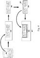
- FIG. 4 illustrates a method of preparing a nanoparticle-based light emitting device that overcomes the problems described above.
- a suspension 401 of nanoparticles in a matrix material precursor is transferred to a mold 402. Once in the mold, the matrix material precursor is converted to the matrix material to yield a molded nanoparticle phosphor 403.
- molded nanoparticle phosphor is schematically represented as being square-shaped in FIG. 4 , but it will be appreciated that the actual shape of molded nanoparticle phosphor 403 will be determined by the shape of mold 402. The disclosure is not limited to any particular shape. Note also that FIGS. 1-4 are not to scale.
- Exemplary matrix materials include resins, polymers, sol gels, epoxies, silicones, (meth)acrylates or the like, or may include silica.
- matrix materials include acrylate polymers (e.g., polymethyl(meth)acrylate, polybutylmethacrylate, polyoctylmethacrylate, alkylcyanoacryaltes, polyethyleneglycol dimethacrylate, polyvinylacetate etc), epoxides (e.g., EPOTEK 301 A+B Thermal curing epoxy, EPOTEK OG112-4 single pot UV curing epoxy, or EX0135A and B Thermal curing epoxy), polyamides, polyimides, polyesters, polycarbonates, polythioethers, polyacrylonitryls, polydienes, polystyrene polybutadiene copolymers (Kratons), pyrelenes, poly-para-xylylene (parylenes), silica, silica-acrylate hybrids
- Matrix material precursors may be any precursor formulation in which the nanoparticles can be suspended or dissolved and which can be converted to the matrix material.
- the matrix material precursor may be a formulation of the corresponding monomer and any additional species, such as photoinitiators, catalysts, and/or crosslinking agents for converting the matrix material precursor to the matrix material.
- the matrix material precursor in which the matrix material is an acrylate polymer, can be a formulation of the appropriate methacrylate monomer, a photoinitiator, and a crosslinking agent.
- the matrix material precursor can be converted to the matrix material by any method known in the art, including by not limited to, photoinitiated polymerization.
- Mold 402 can be any mold having the shape to produce the desired shape of molded nanoparticle phosphor 403. According to one embodiment, mold 402 is itself LED packaging that is substantially identical to the LED packaging to be used in the final nanoparticle light-emitting device. The disclosure is not limited to any particular method of forming molded nanoparticle phosphor 403. Any known molding or casting technique can be used, for example, contact molding, casting, extrusion or injection molding.
- Molded nanoparticle phosphor 403 can be coated with a gas barrier material to yield coated molded nanoparticle phosphor 404.
- the coating is preferably a barrier to the passage of oxygen or any type of oxidizing agent through the primary matrix material.
- the coating may be a barrier to the passage of free radical species through the primary matrix material, and/or is preferably a moisture barrier. It will be appreciated that the gas barrier material may not completely prevent the passage of gas and/or moisture.
- the coating may provide a layer of coating material of any desirable thickness.
- the surface layer coating may be around 1 to 10 nm thick, up to around 400 to 500 nm thick, or more.
- the coating can include an inorganic material, such as a dielectric (insulator), a metal oxide, a metal nitride or a silica-based material (e.g., a glass).
- the inorganic coating may include silica in any appropriate crystalline form.
- the coating may incorporate an inorganic material in combination with an organic or polymeric material.
- the coating is an inorganic/polymer hybrid, such as a silica-acrylate hybrid material.
- the coating includes a polymeric material, which may be a saturated or unsaturated hydrocarbon polymer, or may incorporate one or more heteroatoms (e.g., O, S, N, halo) or heteroatom-containing functional groups (e.g., carbonyl, cyano, ether, epoxide, amide and the like).
- a polymeric material which may be a saturated or unsaturated hydrocarbon polymer, or may incorporate one or more heteroatoms (e.g., O, S, N, halo) or heteroatom-containing functional groups (e.g., carbonyl, cyano, ether, epoxide, amide and the like).
- polymeric coating materials examples include acrylate polymers (e.g., polymethyl(meth)acrylate, polybutylmethacrylate, polyoctylmethacrylate, alkylcyanoacryaltes, polyethyleneglycol dimethacrylate, polyvinylacetate etc), epoxides (e.g., EPOTEK 301 A+B Thermal curing epoxy, EPOTEK OG112-4 single pot UV curing epoxy, or EX0135A and B Thermal curing epoxy), polyamides, polyimides, polyesters, polycarbonates, polythioethers, polyacrylonitryls, polydienes, polystyrene polybutadiene copolymers (Kratons), pyrelenes, poly-para-xylylene (parylenes), polyetheretherketone (PEEK), polyvinylidene fluoride (PVDF), polydivinyl benzene, polyethylene, polypropylene, polyethylene terephthalate (PET)
- Coating 405 can be applied to molded nanoparticle phosphor 403 by any coating method known in the art and in related arts, such as the pharmaceutical arts, wherein coating are commonly applied to tablets and the like. Examples of coating methods include atomic layer deposition (ALD). Other methods include spray coating, evaporative and brush coating.
- ALD atomic layer deposition
- Other methods include spray coating, evaporative and brush coating.
- Coated molded nanoparticle phosphor 404 is inserted into LED packaging 406, which can be filled with an LED encapsulant, such as a silicone or epoxy, and the fabrication of nanoparticle-based light emitting device 407 can be completed according to typical practice in the LED industry.
- LED packaging 406 can be filled with an LED encapsulant, such as a silicone or epoxy, and the fabrication of nanoparticle-based light emitting device 407 can be completed according to typical practice in the LED industry.
- the nanoparticle is a semiconductor material.
- the semiconductor material may incorporate ions from any one or more of groups 2 to 16 of the periodic table, and may include binary, ternary and quaternary materials, that is, materials incorporating two, three or four different ions respectively.
- the nanoparticle may incorporate a semiconductor material, such as, but not limited to, CdS, CdSe, CdTe, ZnS, ZnSe, ZnTe, InP, InAs, InSb, AlP, AIS, AlAs, AISb, GaN, GaP, GaAs, GaSb, PbS, PbSe, Si, Ge and combinations thereof.
- a semiconductor material such as, but not limited to, CdS, CdSe, CdTe, ZnS, ZnSe, ZnTe, InP, InAs, InSb, AlP, AIS, AlAs, AISb, GaN, GaP, GaAs, GaSb, PbS, PbSe, Si, Ge and combinations thereof.
- nanoparticles may have diameters of less than around 100 nm, less than around 50 nm, less than around 20 nm, less than around 15 nm and/or may be in the range of around 2 to 10
- Nanoparticles that include a single semiconductor material may have relatively low quantum efficiencies because of non-radiative electron-hole recombination that occurs at defects and dangling bonds at the surface of the nanoparticles.
- the nanoparticle cores may be at least partially coated with one or more layers (also referred to herein as "shells") of a material different than that of the core, for example a different semiconductor material than that of the "core.”
- the material included in the, or each, shell may incorporate ions from any one or more of groups 2 to 16 of the periodic table.
- each shell may be formed of a different material.
- the core is formed from one of the materials specified above and the shell includes a semiconductor material of larger band-gap energy and similar lattice dimensions as the core material.
- Exemplary shell materials include, but are not limited to, ZnS, ZnO, MgS, MgSe, MgTe and GaN.
- An exemplary multi-shell nanoparticle is InP/ZnS/ZnO. The confinement of charge carriers within the core and away from surface states provides nanoparticles of greater stability and higher quantum yield.
- nanoparticles comprising materials that do not contain cadmium are particularly favored because of increasing concern over potential toxic and environmental effects associated with cadmium.
- cadmium free nanoparticles include nanoparticles comprising semiconductor materials, e.g., ZnS, ZnSe, ZnTe, InP, InAs, InSb, AlP, AIS, AIAs, AISb, GaN, GaP, GaAs, GaSb, PbS, PbSe, Si, Ge, and particularly, nanoparticles comprising cores of one of these materials and one or more shells of another of these materials.
- Molded nanoparticle phosphors of the size of a standard 20 mw LED package were prepared by using an actual LED package as a mold.
- a solution of CFQD in toluene (for example 20 mg inorganic) is dried under vacuum to leave a QDs residue.
- laurylmethacrylate (1.85 ml, 6.6 mmol) is added to a solution of the photoinitiator (Irgacure 819, 9mg) dissolved in the crosslinker trimethylolpropane trimethacrylate (1.06 ml, 3.3 mmol).
- An aliquot of the monomer mixture (1.5-3ul) is used to fill the cup of an LED.
- the filled LED is then irradiated (Hamamatsu uv-LED lamp LC-L2, 365nm, 7500 mW/cm2, 3 minutes).
- the solidified molded nanoparticle phosphor is then removed from the LED by simple tapping and then processed for coating with gas barrier film (using for examples coating methods such as Atomic Layer Deposition-ALD and or high barrier materials like PVOH).
- the coated disc is then inserted into a new LED package that is filled with a proper encapsulating resin.
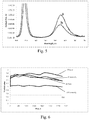
- FIG. 5 shows an emission spectrum produced by a cadmium free quantum dot nanoparticle-based (CFQD) (InP/ZnS) light emitting device using a molded nanoparticle phosphor (curve a), compared to a device using nanoparticles suspended in microbeads (curve b) of the same matrix material.
- the emission luminescence peak at about 630 nm is substantially higher with the molded nanoparticle phosphor device.
- the luminescence intensity is attenuated in the microbead-based device likely due to scattering by the multiple microbeads, as discussed above.
- FIG. 6 shows the efficacy (curve a, the total brightness of the LED based on human eye sensitivity), percent photoluminescence intensity of the QD peak alone (curve b), QD/LED intensity (curve c, the ratio between the QD peak alone and the blue chip peak), and LED intensity (curve d, the blue chip peak alone) a nanoparticle light emitting device using a molded nanoparticle phosphor, as disclosed herein.
Landscapes
- Chemical & Material Sciences (AREA)
- Engineering & Computer Science (AREA)
- Organic Chemistry (AREA)
- Materials Engineering (AREA)
- Inorganic Chemistry (AREA)
- Life Sciences & Earth Sciences (AREA)
- Wood Science & Technology (AREA)
- Chemical Kinetics & Catalysis (AREA)
- Nanotechnology (AREA)
- Crystallography & Structural Chemistry (AREA)
- Manufacturing & Machinery (AREA)
- General Physics & Mathematics (AREA)
- Condensed Matter Physics & Semiconductors (AREA)
- Physics & Mathematics (AREA)
- Led Device Packages (AREA)
- Luminescent Compositions (AREA)
Claims (9)
- Verfahren für die Herstellung eines geformten Nanopartikelphosphors, wobei das Verfahren Folgendes umfasst:das Bereitstellen einer Suspension von Nanopartikeln in einem Matrixmaterialvorläufer; unddas Umwandeln des Matrixmaterialvorläufers in ein Matrixmaterial, um einen geformten Nanopartikelphosphor, der ein Matrixmaterial und die Nanopartikel umfasst, zu ergeben; und das Beschichten des geformten Nanopartikelphosphors mit einem Gasbarrierematerial, wobei das Gasbarrierematerial ein Metalloxid, Metallnitrid, Glas, Epoxy oder Acrylat ist und der Matrixmaterialvorläufer eine Monomerformulierung umfasst.
- Verfahren nach Anspruch 1, wobei das Matrixmaterial ein Polymer oder ein Sol-Gel ist.
- Verfahren nach Anspruch 1, wobei das Matrixmaterial ein Epoxy, Silicon oder Acrylat ist.
- Verfahren nach Anspruch 1, wobei der Matrixmaterialvorläufer ferner einen Katalysator, ein Vernetzungsmittel oder einen Initiator umfasst.
- Verfahren nach Anspruch 1, wobei das Umwandeln der Suspension in einen geformten Nanopartikelphosphor das Polymerisationsformen, Kontaktformen, Gießen, Extrudieren oder Injektionsformen umfasst.
- Verfahren nach Anspruch 1, wobei das Beschichten des geformten Nanopartikelphosphors mit einem Gasbarrierematerial das Atomlagenabscheiden, Pinselbeschichten, verdampfendes Beschichten oder Spritzbeschichten umfasst.
- Geformter Nanopartikelphosphor, der dem Verfahren nach einem der Ansprüche 1-6 entsprechend hergestellt wird.
- Lichtemittierende Vorrichtung auf der Basis von Nanopartikeln, umfassend einen geformten Nanopartikelphosphor, der dem Verfahren nach einem der Ansprüche 1-6 entsprechend hergestellt wird.
- Verfahren für die Herstellung einer lichtemittierenden Vorrichtung auf der Basis von Nanopartikeln umfassend:das Herstellen eines geformten Nanopartikelphosphors dem Verfahren nach einem der Ansprüche 1-6 entsprechend; unddas Integrieren des geformten Nanopartikelphosphors in eine lichtemittierende Diodenpackung.
Applications Claiming Priority (2)
| Application Number | Priority Date | Filing Date | Title |
|---|---|---|---|
| US201261588377P | 2012-01-19 | 2012-01-19 | |
| PCT/IB2013/000408 WO2013108125A2 (en) | 2012-01-19 | 2013-01-17 | Molded nanoparticle phosphor for light emitting applications |
Publications (2)
| Publication Number | Publication Date |
|---|---|
| EP2804925A2 EP2804925A2 (de) | 2014-11-26 |
| EP2804925B1 true EP2804925B1 (de) | 2016-12-28 |
Family
ID=48050860
Family Applications (1)
| Application Number | Title | Priority Date | Filing Date |
|---|---|---|---|
| EP13714996.9A Active EP2804925B1 (de) | 2012-01-19 | 2013-01-17 | Geformter nanopartikelphosphor für lichtemittierende anwendungen |
Country Status (6)
| Country | Link |
|---|---|
| US (2) | US10066158B2 (de) |
| EP (1) | EP2804925B1 (de) |
| JP (2) | JP6322581B2 (de) |
| KR (3) | KR101645263B1 (de) |
| CN (2) | CN107254206B (de) |
| WO (1) | WO2013108125A2 (de) |
Cited By (1)
| Publication number | Priority date | Publication date | Assignee | Title |
|---|---|---|---|---|
| WO2018190449A1 (ko) * | 2017-04-13 | 2018-10-18 | (주)라이타이저코리아 | 라운드 칩 스케일 패키지 및 그의 제조 방법 |
Families Citing this family (31)
| Publication number | Priority date | Publication date | Assignee | Title |
|---|---|---|---|---|
| WO2011047385A1 (en) | 2009-10-17 | 2011-04-21 | Qd Vision, Inc. | An optical, component, products including same, and methods for making same |
| DE102013206077A1 (de) * | 2013-04-05 | 2014-10-09 | Fraunhofer-Gesellschaft zur Förderung der angewandten Forschung e.V. | Blau-emittierende Leuchtdioden auf Basis von Zinkselenid-Quantenpunkten |
| EP3033552B1 (de) | 2013-08-16 | 2023-05-31 | Samsung Electronics Co., Ltd. | Verfahren zur herstellung von optischen komponenten und produkte damit |
| JP6469108B2 (ja) * | 2013-11-19 | 2019-02-13 | 三星電子株式会社Samsung Electronics Co.,Ltd. | ルミネッセンス粒子、これを含む材料および製品、ならびに方法 |
| US9470399B1 (en) * | 2013-12-13 | 2016-10-18 | Amazon Technologies, Inc. | Light-emitting polymer films, articles containing same, and methods of making |
| US20150316219A1 (en) * | 2014-05-01 | 2015-11-05 | CoreLed Systems, LLC | High-pass filter for led lighting |
| US9466771B2 (en) | 2014-07-23 | 2016-10-11 | Osram Sylvania Inc. | Wavelength converters and methods for making the same |
| EP3179524B1 (de) * | 2014-08-06 | 2024-09-04 | Toppan Inc. | Harzformartikel, verfahren zur herstellung davon, wellenlängenumwandlungselement und beleuchtungselement |
| EP3217444A4 (de) * | 2014-11-04 | 2018-08-22 | NS Materials Inc. | Wellenlängenumwandlungselement, lichtemittierende vorrichtung damit, lichtemittierendes element, lichtquellenvorrichtung, anzeigevorrichtung lichtleiterelement und verfahren zur herstellung eines wellenlängenumwandlungselements |
| US9401468B2 (en) | 2014-12-24 | 2016-07-26 | GE Lighting Solutions, LLC | Lamp with LED chips cooled by a phase transformation loop |
| JP6372394B2 (ja) * | 2015-02-27 | 2018-08-15 | 豊田合成株式会社 | 発光装置 |
| US10174886B2 (en) * | 2015-07-31 | 2019-01-08 | Sharp Kabushiki Kaisha | Wavelength conversion member and light emitting device |
| KR102449686B1 (ko) * | 2015-09-18 | 2022-09-30 | 엘지전자 주식회사 | 광 변환 복합체, 이를 포함하는 광 변환 부재, 표시장치 및 발광소자 패키지및 이의 제조방법 |
| TW201729901A (zh) | 2015-12-02 | 2017-09-01 | 奈米系統股份有限公司 | 於顯示裝置中基於量子點之色轉換層 |
| US20170167693A1 (en) * | 2015-12-15 | 2017-06-15 | Sharp Kabushiki Kaisha | Light emitting structure and light emitting device using the same |
| US20170166807A1 (en) * | 2015-12-15 | 2017-06-15 | Sharp Kabushiki Kaisha | Phosphor containing particle, and light emitting device and phosphor containing sheet using the same |
| CN105602546B (zh) * | 2015-12-30 | 2018-06-22 | 马鞍山蓝信环保科技有限公司 | 用于3d打印的量子点发光复合物及其制备方法 |
| CN116898966A (zh) | 2016-02-02 | 2023-10-20 | 免疫之光有限责任公司 | 含磷光体之药物激活剂、其悬液、包含悬液的系统及使用方法 |
| WO2017197392A1 (en) | 2016-05-13 | 2017-11-16 | Osram Sylvania Inc. | Wavelength converters including a porous matrix, lighting devices including the same, and methods of forming the same |
| US10475967B2 (en) | 2017-04-27 | 2019-11-12 | Osram Opto Semiconductors Gmbh | Wavelength converters with improved thermal conductivity and lighting devices including the same |
| JP6712968B2 (ja) * | 2017-06-09 | 2020-06-24 | シャープ株式会社 | 蛍光体含有粒子およびそれを用いた発光装置、蛍光体含有シート |
| US10483441B2 (en) * | 2017-06-09 | 2019-11-19 | Sharp Kabushiki Kaisha | Phosphor containing particle, and light emitting device and phosphor containing sheet using the same |
| US10752834B2 (en) * | 2018-05-17 | 2020-08-25 | Chung Yuan Christian University | Composite fluorescent gold nanoclusters with high quantum yield and method for manufacturing the same |
| KR102138256B1 (ko) | 2018-09-13 | 2020-08-13 | 한국과학기술연구원 | 케스페이즈-1 활성 측정용 프로브, 이를 포함하는 염증성 질환 진단용 조성물 |
| US10756243B1 (en) * | 2019-03-04 | 2020-08-25 | Chung Yuan Christian University | Light-emitting diode package structure and method for manufacturing the same |
| KR20220016465A (ko) * | 2019-05-31 | 2022-02-09 | 소에이 가가쿠 고교 가부시키가이샤 | 반도체 나노입자 복합체 조성물, 희석 조성물, 반도체 나노입자 복합체 경화막, 반도체 나노입자 복합체 패터닝막, 표시 소자, 및 반도체 나노입자 복합체 분산액 |
| KR102318955B1 (ko) * | 2020-01-09 | 2021-10-28 | 공주대학교 산학협력단 | 형광 에폭시 투명목재 제조방법 및 이로부터 제조된 형광 에폭시 투명목재 |
| CN111960821B (zh) * | 2020-07-27 | 2022-04-12 | 苏州瑞玛精密工业股份有限公司 | 一种微波介质陶瓷材料及其制备方法和应用 |
| CA3208782A1 (en) * | 2021-02-05 | 2022-08-11 | Universiteit Gent | A method to prepare pockets of encapsulated material comprising a core surrounded by an encapsulation |
| CN113861983B (zh) * | 2021-09-26 | 2023-06-23 | 广州华商职业学院 | 一种高光效量子点光转化涂层的制备方法及其应用 |
| CN118985312A (zh) * | 2024-08-07 | 2024-11-22 | 华南农业大学 | 一种单色、多色或变色蓄光型发光植物及其制备方法 |
Family Cites Families (23)
| Publication number | Priority date | Publication date | Assignee | Title |
|---|---|---|---|---|
| EP0406554A3 (en) * | 1989-07-06 | 1991-08-28 | Samsung Electron Devices Co., Ltd. | Phosphors and color cathode ray tubes using same |
| JP3900617B2 (ja) * | 1997-09-17 | 2007-04-04 | カシオ計算機株式会社 | 発光素子及び発光素子用の保護材料 |
| US6515314B1 (en) * | 2000-11-16 | 2003-02-04 | General Electric Company | Light-emitting device with organic layer doped with photoluminescent material |
| US6822391B2 (en) * | 2001-02-21 | 2004-11-23 | Semiconductor Energy Laboratory Co., Ltd. | Light emitting device, electronic equipment, and method of manufacturing thereof |
| CN1646613A (zh) * | 2002-02-19 | 2005-07-27 | 光子-X有限公司 | 应用于光学的聚合物纳米复合材料 |
| JP2003272827A (ja) * | 2002-03-13 | 2003-09-26 | Matsushita Electric Ind Co Ltd | 有機発光素子及びその製造方法 |
| US7915085B2 (en) * | 2003-09-18 | 2011-03-29 | Cree, Inc. | Molded chip fabrication method |
| US20050238803A1 (en) * | 2003-11-12 | 2005-10-27 | Tremel James D | Method for adhering getter material to a surface for use in electronic devices |
| US7573072B2 (en) * | 2004-03-10 | 2009-08-11 | Lumination Llc | Phosphor and blends thereof for use in LEDs |
| US20060083694A1 (en) * | 2004-08-07 | 2006-04-20 | Cabot Corporation | Multi-component particles comprising inorganic nanoparticles distributed in an organic matrix and processes for making and using same |
| US7723408B2 (en) * | 2005-02-16 | 2010-05-25 | Georgia Tech Research Corporation | Composite materials having low filler percolation thresholds and methods of controlling filler interconnectivity |
| US8057664B2 (en) * | 2005-11-17 | 2011-11-15 | Exxonmobil Chemical Patents, Inc. | Process for reducing bromine index of hydrocarbon feedstocks |
| WO2008082362A1 (en) * | 2006-12-28 | 2008-07-10 | Agency For Science, Technology And Research | Encapsulated device with integrated gas permeation sensor |
| KR101686669B1 (ko) | 2007-03-19 | 2016-12-14 | 나노시스, 인크. | 나노크리스털을 캡슐화하는 방법 |
| US20080230750A1 (en) * | 2007-03-20 | 2008-09-25 | Evident Technologies, Inc. | Powdered quantum dots |
| JP5156947B2 (ja) * | 2007-03-22 | 2013-03-06 | 国立大学法人 熊本大学 | 酸化物ナノシート蛍光体及びその製造方法 |
| JP4888280B2 (ja) * | 2007-08-28 | 2012-02-29 | パナソニック電工株式会社 | 発光装置 |
| RU2011115069A (ru) * | 2008-09-16 | 2012-10-27 | Конинклейке Филипс Электроникс Н.В. (Nl) | Полимерные элементы, изменяющие длину волны |
| GB0821122D0 (en) * | 2008-11-19 | 2008-12-24 | Nanoco Technologies Ltd | Semiconductor nanoparticle - based light emitting devices and associated materials and methods |
| TW201034256A (en) * | 2008-12-11 | 2010-09-16 | Illumitex Inc | Systems and methods for packaging light-emitting diode devices |
| KR101525523B1 (ko) * | 2008-12-22 | 2015-06-03 | 삼성전자 주식회사 | 반도체 나노 결정 복합체 |
| GB0916700D0 (en) | 2009-09-23 | 2009-11-04 | Nanoco Technologies Ltd | Semiconductor nanoparticle-based materials |
| GB0916699D0 (en) * | 2009-09-23 | 2009-11-04 | Nanoco Technologies Ltd | Semiconductor nanoparticle-based materials |
-
2013
- 2013-01-17 EP EP13714996.9A patent/EP2804925B1/de active Active
- 2013-01-17 CN CN201710402088.3A patent/CN107254206B/zh active Active
- 2013-01-17 CN CN201380005786.XA patent/CN104066814B/zh active Active
- 2013-01-17 KR KR1020147020064A patent/KR101645263B1/ko active Active
- 2013-01-17 WO PCT/IB2013/000408 patent/WO2013108125A2/en not_active Ceased
- 2013-01-17 US US13/743,414 patent/US10066158B2/en active Active
- 2013-01-17 JP JP2014552711A patent/JP6322581B2/ja active Active
- 2013-01-17 KR KR1020177006272A patent/KR101971611B1/ko active Active
- 2013-01-17 KR KR1020167020751A patent/KR20160095187A/ko not_active Ceased
-
2017
- 2017-12-05 JP JP2017233026A patent/JP6481015B2/ja active Active
-
2018
- 2018-08-10 US US16/101,052 patent/US10461224B2/en active Active
Non-Patent Citations (1)
| Title |
|---|
| None * |
Cited By (2)
| Publication number | Priority date | Publication date | Assignee | Title |
|---|---|---|---|---|
| WO2018190449A1 (ko) * | 2017-04-13 | 2018-10-18 | (주)라이타이저코리아 | 라운드 칩 스케일 패키지 및 그의 제조 방법 |
| US10950762B2 (en) | 2017-04-13 | 2021-03-16 | Lightizer Co., Ltd | Round chip scale package and manufacturing method therefor |
Also Published As
| Publication number | Publication date |
|---|---|
| JP6322581B2 (ja) | 2018-05-09 |
| CN107254206B (zh) | 2021-04-27 |
| KR101971611B1 (ko) | 2019-04-24 |
| US20180346805A1 (en) | 2018-12-06 |
| JP2015509125A (ja) | 2015-03-26 |
| KR20160095187A (ko) | 2016-08-10 |
| HK1203998A1 (en) | 2015-11-06 |
| CN104066814B (zh) | 2017-06-16 |
| US20130189803A1 (en) | 2013-07-25 |
| WO2013108125A3 (en) | 2013-10-24 |
| US10066158B2 (en) | 2018-09-04 |
| CN104066814A (zh) | 2014-09-24 |
| KR101645263B1 (ko) | 2016-08-03 |
| KR20140108299A (ko) | 2014-09-05 |
| US10461224B2 (en) | 2019-10-29 |
| EP2804925A2 (de) | 2014-11-26 |
| WO2013108125A2 (en) | 2013-07-25 |
| JP2018080337A (ja) | 2018-05-24 |
| JP6481015B2 (ja) | 2019-03-13 |
| KR20170029653A (ko) | 2017-03-15 |
| CN107254206A (zh) | 2017-10-17 |
Similar Documents
| Publication | Publication Date | Title |
|---|---|---|
| US10461224B2 (en) | Molded nanoparticle phosphor for light emitting applications | |
| JP6631973B2 (ja) | 量子ドット複合材料ならびにその製造方法および用途 | |
| US9053959B2 (en) | Semiconductor light converting construction | |
| CN102124583B (zh) | 半导体光转换构造 | |
| TWI680178B (zh) | 量子點材料及其製備方法 | |
| US8324000B2 (en) | Method of fabricating light extractor | |
| TW201530829A (zh) | 含有量子點磷光體的發光二極體蓋 | |
| CN102648536A (zh) | 包含添加剂的基于封装半导体纳米粒子的材料 | |
| CN102124581B (zh) | 光转换构造 | |
| KR101413660B1 (ko) | 발광다이오드용 양자점-고분자 복합체 플레이트 및 그 제조 방법 | |
| HK1203998B (en) | Molded nanoparticle phosphor for light emitting applications | |
| US20110101402A1 (en) | Semiconductor light converting construction | |
| KR101436099B1 (ko) | Led용 이중 양자점-고분자 복합체 플레이트 및 그 제조 방법 |
Legal Events
| Date | Code | Title | Description |
|---|---|---|---|
| PUAI | Public reference made under article 153(3) epc to a published international application that has entered the european phase |
Free format text: ORIGINAL CODE: 0009012 |
|
| 17P | Request for examination filed |
Effective date: 20140619 |
|
| AK | Designated contracting states |
Kind code of ref document: A2 Designated state(s): AL AT BE BG CH CY CZ DE DK EE ES FI FR GB GR HR HU IE IS IT LI LT LU LV MC MK MT NL NO PL PT RO RS SE SI SK SM TR |
|
| DAX | Request for extension of the european patent (deleted) | ||
| 17Q | First examination report despatched |
Effective date: 20150820 |
|
| REG | Reference to a national code |
Ref country code: HK Ref legal event code: DE Ref document number: 1203998 Country of ref document: HK |
|
| GRAP | Despatch of communication of intention to grant a patent |
Free format text: ORIGINAL CODE: EPIDOSNIGR1 |
|
| INTG | Intention to grant announced |
Effective date: 20160914 |
|
| GRAS | Grant fee paid |
Free format text: ORIGINAL CODE: EPIDOSNIGR3 |
|
| GRAA | (expected) grant |
Free format text: ORIGINAL CODE: 0009210 |
|
| AK | Designated contracting states |
Kind code of ref document: B1 Designated state(s): AL AT BE BG CH CY CZ DE DK EE ES FI FR GB GR HR HU IE IS IT LI LT LU LV MC MK MT NL NO PL PT RO RS SE SI SK SM TR |
|
| REG | Reference to a national code |
Ref country code: GB Ref legal event code: FG4D |
|
| REG | Reference to a national code |
Ref country code: CH Ref legal event code: EP |
|
| REG | Reference to a national code |
Ref country code: AT Ref legal event code: REF Ref document number: 857284 Country of ref document: AT Kind code of ref document: T Effective date: 20170115 |
|
| REG | Reference to a national code |
Ref country code: IE Ref legal event code: FG4D |
|
| REG | Reference to a national code |
Ref country code: DE Ref legal event code: R096 Ref document number: 602013015851 Country of ref document: DE |
|
| PG25 | Lapsed in a contracting state [announced via postgrant information from national office to epo] |
Ref country code: LV Free format text: LAPSE BECAUSE OF FAILURE TO SUBMIT A TRANSLATION OF THE DESCRIPTION OR TO PAY THE FEE WITHIN THE PRESCRIBED TIME-LIMIT Effective date: 20161228 |
|
| REG | Reference to a national code |
Ref country code: FR Ref legal event code: PLFP Year of fee payment: 5 |
|
| REG | Reference to a national code |
Ref country code: NL Ref legal event code: FP |
|
| REG | Reference to a national code |
Ref country code: LT Ref legal event code: MG4D |
|
| PG25 | Lapsed in a contracting state [announced via postgrant information from national office to epo] |
Ref country code: LT Free format text: LAPSE BECAUSE OF FAILURE TO SUBMIT A TRANSLATION OF THE DESCRIPTION OR TO PAY THE FEE WITHIN THE PRESCRIBED TIME-LIMIT Effective date: 20161228 Ref country code: GR Free format text: LAPSE BECAUSE OF FAILURE TO SUBMIT A TRANSLATION OF THE DESCRIPTION OR TO PAY THE FEE WITHIN THE PRESCRIBED TIME-LIMIT Effective date: 20170329 Ref country code: SE Free format text: LAPSE BECAUSE OF FAILURE TO SUBMIT A TRANSLATION OF THE DESCRIPTION OR TO PAY THE FEE WITHIN THE PRESCRIBED TIME-LIMIT Effective date: 20161228 Ref country code: NO Free format text: LAPSE BECAUSE OF FAILURE TO SUBMIT A TRANSLATION OF THE DESCRIPTION OR TO PAY THE FEE WITHIN THE PRESCRIBED TIME-LIMIT Effective date: 20170328 |
|
| REG | Reference to a national code |
Ref country code: AT Ref legal event code: MK05 Ref document number: 857284 Country of ref document: AT Kind code of ref document: T Effective date: 20161228 |
|
| PG25 | Lapsed in a contracting state [announced via postgrant information from national office to epo] |
Ref country code: HR Free format text: LAPSE BECAUSE OF FAILURE TO SUBMIT A TRANSLATION OF THE DESCRIPTION OR TO PAY THE FEE WITHIN THE PRESCRIBED TIME-LIMIT Effective date: 20161228 Ref country code: BE Free format text: LAPSE BECAUSE OF NON-PAYMENT OF DUE FEES Effective date: 20170131 Ref country code: RS Free format text: LAPSE BECAUSE OF FAILURE TO SUBMIT A TRANSLATION OF THE DESCRIPTION OR TO PAY THE FEE WITHIN THE PRESCRIBED TIME-LIMIT Effective date: 20161228 Ref country code: FI Free format text: LAPSE BECAUSE OF FAILURE TO SUBMIT A TRANSLATION OF THE DESCRIPTION OR TO PAY THE FEE WITHIN THE PRESCRIBED TIME-LIMIT Effective date: 20161228 |
|
| PG25 | Lapsed in a contracting state [announced via postgrant information from national office to epo] |
Ref country code: EE Free format text: LAPSE BECAUSE OF FAILURE TO SUBMIT A TRANSLATION OF THE DESCRIPTION OR TO PAY THE FEE WITHIN THE PRESCRIBED TIME-LIMIT Effective date: 20161228 Ref country code: IS Free format text: LAPSE BECAUSE OF FAILURE TO SUBMIT A TRANSLATION OF THE DESCRIPTION OR TO PAY THE FEE WITHIN THE PRESCRIBED TIME-LIMIT Effective date: 20170428 Ref country code: RO Free format text: LAPSE BECAUSE OF FAILURE TO SUBMIT A TRANSLATION OF THE DESCRIPTION OR TO PAY THE FEE WITHIN THE PRESCRIBED TIME-LIMIT Effective date: 20161228 Ref country code: CZ Free format text: LAPSE BECAUSE OF FAILURE TO SUBMIT A TRANSLATION OF THE DESCRIPTION OR TO PAY THE FEE WITHIN THE PRESCRIBED TIME-LIMIT Effective date: 20161228 Ref country code: SK Free format text: LAPSE BECAUSE OF FAILURE TO SUBMIT A TRANSLATION OF THE DESCRIPTION OR TO PAY THE FEE WITHIN THE PRESCRIBED TIME-LIMIT Effective date: 20161228 |
|
| PG25 | Lapsed in a contracting state [announced via postgrant information from national office to epo] |
Ref country code: AT Free format text: LAPSE BECAUSE OF FAILURE TO SUBMIT A TRANSLATION OF THE DESCRIPTION OR TO PAY THE FEE WITHIN THE PRESCRIBED TIME-LIMIT Effective date: 20161228 Ref country code: BE Free format text: LAPSE BECAUSE OF FAILURE TO SUBMIT A TRANSLATION OF THE DESCRIPTION OR TO PAY THE FEE WITHIN THE PRESCRIBED TIME-LIMIT Effective date: 20161228 Ref country code: ES Free format text: LAPSE BECAUSE OF FAILURE TO SUBMIT A TRANSLATION OF THE DESCRIPTION OR TO PAY THE FEE WITHIN THE PRESCRIBED TIME-LIMIT Effective date: 20161228 Ref country code: BG Free format text: LAPSE BECAUSE OF FAILURE TO SUBMIT A TRANSLATION OF THE DESCRIPTION OR TO PAY THE FEE WITHIN THE PRESCRIBED TIME-LIMIT Effective date: 20170328 Ref country code: IT Free format text: LAPSE BECAUSE OF FAILURE TO SUBMIT A TRANSLATION OF THE DESCRIPTION OR TO PAY THE FEE WITHIN THE PRESCRIBED TIME-LIMIT Effective date: 20161228 Ref country code: PL Free format text: LAPSE BECAUSE OF FAILURE TO SUBMIT A TRANSLATION OF THE DESCRIPTION OR TO PAY THE FEE WITHIN THE PRESCRIBED TIME-LIMIT Effective date: 20161228 Ref country code: SM Free format text: LAPSE BECAUSE OF FAILURE TO SUBMIT A TRANSLATION OF THE DESCRIPTION OR TO PAY THE FEE WITHIN THE PRESCRIBED TIME-LIMIT Effective date: 20161228 Ref country code: PT Free format text: LAPSE BECAUSE OF FAILURE TO SUBMIT A TRANSLATION OF THE DESCRIPTION OR TO PAY THE FEE WITHIN THE PRESCRIBED TIME-LIMIT Effective date: 20170428 |
|
| REG | Reference to a national code |
Ref country code: CH Ref legal event code: PL |
|
| PG25 | Lapsed in a contracting state [announced via postgrant information from national office to epo] |
Ref country code: MC Free format text: LAPSE BECAUSE OF FAILURE TO SUBMIT A TRANSLATION OF THE DESCRIPTION OR TO PAY THE FEE WITHIN THE PRESCRIBED TIME-LIMIT Effective date: 20161228 |
|
| REG | Reference to a national code |
Ref country code: DE Ref legal event code: R097 Ref document number: 602013015851 Country of ref document: DE |
|
| PG25 | Lapsed in a contracting state [announced via postgrant information from national office to epo] |
Ref country code: CH Free format text: LAPSE BECAUSE OF NON-PAYMENT OF DUE FEES Effective date: 20170131 Ref country code: LI Free format text: LAPSE BECAUSE OF NON-PAYMENT OF DUE FEES Effective date: 20170131 |
|
| REG | Reference to a national code |
Ref country code: IE Ref legal event code: MM4A |
|
| PLBE | No opposition filed within time limit |
Free format text: ORIGINAL CODE: 0009261 |
|
| STAA | Information on the status of an ep patent application or granted ep patent |
Free format text: STATUS: NO OPPOSITION FILED WITHIN TIME LIMIT |
|
| PG25 | Lapsed in a contracting state [announced via postgrant information from national office to epo] |
Ref country code: LU Free format text: LAPSE BECAUSE OF NON-PAYMENT OF DUE FEES Effective date: 20170117 Ref country code: DK Free format text: LAPSE BECAUSE OF FAILURE TO SUBMIT A TRANSLATION OF THE DESCRIPTION OR TO PAY THE FEE WITHIN THE PRESCRIBED TIME-LIMIT Effective date: 20161228 |
|
| 26N | No opposition filed |
Effective date: 20170929 |
|
| REG | Reference to a national code |
Ref country code: HK Ref legal event code: GR Ref document number: 1203998 Country of ref document: HK |
|
| REG | Reference to a national code |
Ref country code: FR Ref legal event code: PLFP Year of fee payment: 6 |
|
| PG25 | Lapsed in a contracting state [announced via postgrant information from national office to epo] |
Ref country code: SI Free format text: LAPSE BECAUSE OF FAILURE TO SUBMIT A TRANSLATION OF THE DESCRIPTION OR TO PAY THE FEE WITHIN THE PRESCRIBED TIME-LIMIT Effective date: 20161228 Ref country code: IE Free format text: LAPSE BECAUSE OF NON-PAYMENT OF DUE FEES Effective date: 20170117 |
|
| PG25 | Lapsed in a contracting state [announced via postgrant information from national office to epo] |
Ref country code: MT Free format text: LAPSE BECAUSE OF NON-PAYMENT OF DUE FEES Effective date: 20170117 |
|
| PG25 | Lapsed in a contracting state [announced via postgrant information from national office to epo] |
Ref country code: HU Free format text: LAPSE BECAUSE OF FAILURE TO SUBMIT A TRANSLATION OF THE DESCRIPTION OR TO PAY THE FEE WITHIN THE PRESCRIBED TIME-LIMIT; INVALID AB INITIO Effective date: 20130117 |
|
| PG25 | Lapsed in a contracting state [announced via postgrant information from national office to epo] |
Ref country code: CY Free format text: LAPSE BECAUSE OF FAILURE TO SUBMIT A TRANSLATION OF THE DESCRIPTION OR TO PAY THE FEE WITHIN THE PRESCRIBED TIME-LIMIT Effective date: 20161228 |
|
| PG25 | Lapsed in a contracting state [announced via postgrant information from national office to epo] |
Ref country code: MK Free format text: LAPSE BECAUSE OF FAILURE TO SUBMIT A TRANSLATION OF THE DESCRIPTION OR TO PAY THE FEE WITHIN THE PRESCRIBED TIME-LIMIT Effective date: 20161228 |
|
| PG25 | Lapsed in a contracting state [announced via postgrant information from national office to epo] |
Ref country code: TR Free format text: LAPSE BECAUSE OF FAILURE TO SUBMIT A TRANSLATION OF THE DESCRIPTION OR TO PAY THE FEE WITHIN THE PRESCRIBED TIME-LIMIT Effective date: 20161228 |
|
| PG25 | Lapsed in a contracting state [announced via postgrant information from national office to epo] |
Ref country code: AL Free format text: LAPSE BECAUSE OF FAILURE TO SUBMIT A TRANSLATION OF THE DESCRIPTION OR TO PAY THE FEE WITHIN THE PRESCRIBED TIME-LIMIT Effective date: 20161228 |
|
| P01 | Opt-out of the competence of the unified patent court (upc) registered |
Effective date: 20230525 |
|
| PGFP | Annual fee paid to national office [announced via postgrant information from national office to epo] |
Ref country code: NL Payment date: 20251126 Year of fee payment: 14 |
|
| PGFP | Annual fee paid to national office [announced via postgrant information from national office to epo] |
Ref country code: GB Payment date: 20251127 Year of fee payment: 14 |
|
| PGFP | Annual fee paid to national office [announced via postgrant information from national office to epo] |
Ref country code: FR Payment date: 20251124 Year of fee payment: 14 |
|
| PGFP | Annual fee paid to national office [announced via postgrant information from national office to epo] |
Ref country code: DE Payment date: 20251126 Year of fee payment: 14 |