EP2805351B1 - Resistive speicherzellenstrukturen und verfahren - Google Patents
Resistive speicherzellenstrukturen und verfahren Download PDFInfo
- Publication number
- EP2805351B1 EP2805351B1 EP13739105.8A EP13739105A EP2805351B1 EP 2805351 B1 EP2805351 B1 EP 2805351B1 EP 13739105 A EP13739105 A EP 13739105A EP 2805351 B1 EP2805351 B1 EP 2805351B1
- Authority
- EP
- European Patent Office
- Prior art keywords
- array
- region
- resistance variable
- memory cells
- resistive memory
- Prior art date
- Legal status (The legal status is an assumption and is not a legal conclusion. Google has not performed a legal analysis and makes no representation as to the accuracy of the status listed.)
- Active
Links
Images


Classifications
-
- H—ELECTRICITY
- H10—SEMICONDUCTOR DEVICES; ELECTRIC SOLID-STATE DEVICES NOT OTHERWISE PROVIDED FOR
- H10B—ELECTRONIC MEMORY DEVICES
- H10B63/00—Resistance change memory devices, e.g. resistive RAM [ReRAM] devices
- H10B63/80—Arrangements comprising multiple bistable or multi-stable switching components of the same type on a plane parallel to the substrate, e.g. cross-point arrays
-
- H—ELECTRICITY
- H10—SEMICONDUCTOR DEVICES; ELECTRIC SOLID-STATE DEVICES NOT OTHERWISE PROVIDED FOR
- H10B—ELECTRONIC MEMORY DEVICES
- H10B53/00—Ferroelectric RAM [FeRAM] devices comprising ferroelectric memory capacitors
- H10B53/30—Ferroelectric RAM [FeRAM] devices comprising ferroelectric memory capacitors characterised by the memory core region
-
- H—ELECTRICITY
- H10—SEMICONDUCTOR DEVICES; ELECTRIC SOLID-STATE DEVICES NOT OTHERWISE PROVIDED FOR
- H10B—ELECTRONIC MEMORY DEVICES
- H10B63/00—Resistance change memory devices, e.g. resistive RAM [ReRAM] devices
- H10B63/10—Phase change RAM [PCRAM, PRAM] devices
-
- H—ELECTRICITY
- H10—SEMICONDUCTOR DEVICES; ELECTRIC SOLID-STATE DEVICES NOT OTHERWISE PROVIDED FOR
- H10N—ELECTRIC SOLID-STATE DEVICES NOT OTHERWISE PROVIDED FOR
- H10N70/00—Solid-state devices having no potential barriers, and specially adapted for rectifying, amplifying, oscillating or switching
- H10N70/011—Manufacture or treatment of multistable switching devices
- H10N70/041—Modification of switching materials after formation, e.g. doping
- H10N70/043—Modification of switching materials after formation, e.g. doping by implantation
-
- H—ELECTRICITY
- H10—SEMICONDUCTOR DEVICES; ELECTRIC SOLID-STATE DEVICES NOT OTHERWISE PROVIDED FOR
- H10N—ELECTRIC SOLID-STATE DEVICES NOT OTHERWISE PROVIDED FOR
- H10N70/00—Solid-state devices having no potential barriers, and specially adapted for rectifying, amplifying, oscillating or switching
- H10N70/011—Manufacture or treatment of multistable switching devices
- H10N70/061—Shaping switching materials
- H10N70/063—Shaping switching materials by etching of pre-deposited switching material layers, e.g. lithography
-
- H—ELECTRICITY
- H10—SEMICONDUCTOR DEVICES; ELECTRIC SOLID-STATE DEVICES NOT OTHERWISE PROVIDED FOR
- H10N—ELECTRIC SOLID-STATE DEVICES NOT OTHERWISE PROVIDED FOR
- H10N70/00—Solid-state devices having no potential barriers, and specially adapted for rectifying, amplifying, oscillating or switching
- H10N70/011—Manufacture or treatment of multistable switching devices
- H10N70/061—Shaping switching materials
- H10N70/066—Shaping switching materials by filling of openings, e.g. damascene method
-
- H—ELECTRICITY
- H10—SEMICONDUCTOR DEVICES; ELECTRIC SOLID-STATE DEVICES NOT OTHERWISE PROVIDED FOR
- H10N—ELECTRIC SOLID-STATE DEVICES NOT OTHERWISE PROVIDED FOR
- H10N70/00—Solid-state devices having no potential barriers, and specially adapted for rectifying, amplifying, oscillating or switching
- H10N70/20—Multistable switching devices, e.g. memristors
- H10N70/231—Multistable switching devices, e.g. memristors based on solid-state phase change, e.g. between amorphous and crystalline phases, Ovshinsky effect
-
- H—ELECTRICITY
- H10—SEMICONDUCTOR DEVICES; ELECTRIC SOLID-STATE DEVICES NOT OTHERWISE PROVIDED FOR
- H10N—ELECTRIC SOLID-STATE DEVICES NOT OTHERWISE PROVIDED FOR
- H10N70/00—Solid-state devices having no potential barriers, and specially adapted for rectifying, amplifying, oscillating or switching
- H10N70/801—Constructional details of multistable switching devices
- H10N70/821—Device geometry
- H10N70/826—Device geometry adapted for essentially vertical current flow, e.g. sandwich or pillar type devices
-
- H—ELECTRICITY
- H10—SEMICONDUCTOR DEVICES; ELECTRIC SOLID-STATE DEVICES NOT OTHERWISE PROVIDED FOR
- H10N—ELECTRIC SOLID-STATE DEVICES NOT OTHERWISE PROVIDED FOR
- H10N70/00—Solid-state devices having no potential barriers, and specially adapted for rectifying, amplifying, oscillating or switching
- H10N70/801—Constructional details of multistable switching devices
- H10N70/841—Electrodes
- H10N70/8413—Electrodes adapted for resistive heating
-
- H—ELECTRICITY
- H10—SEMICONDUCTOR DEVICES; ELECTRIC SOLID-STATE DEVICES NOT OTHERWISE PROVIDED FOR
- H10N—ELECTRIC SOLID-STATE DEVICES NOT OTHERWISE PROVIDED FOR
- H10N70/00—Solid-state devices having no potential barriers, and specially adapted for rectifying, amplifying, oscillating or switching
- H10N70/801—Constructional details of multistable switching devices
- H10N70/861—Thermal details
- H10N70/8613—Heating or cooling means other than resistive heating electrodes, e.g. heater in parallel
-
- H—ELECTRICITY
- H10—SEMICONDUCTOR DEVICES; ELECTRIC SOLID-STATE DEVICES NOT OTHERWISE PROVIDED FOR
- H10N—ELECTRIC SOLID-STATE DEVICES NOT OTHERWISE PROVIDED FOR
- H10N70/00—Solid-state devices having no potential barriers, and specially adapted for rectifying, amplifying, oscillating or switching
- H10N70/801—Constructional details of multistable switching devices
- H10N70/881—Switching materials
- H10N70/882—Compounds of sulfur, selenium or tellurium, e.g. chalcogenides
- H10N70/8828—Tellurides, e.g. GeSbTe
-
- H—ELECTRICITY
- H10—SEMICONDUCTOR DEVICES; ELECTRIC SOLID-STATE DEVICES NOT OTHERWISE PROVIDED FOR
- H10B—ELECTRONIC MEMORY DEVICES
- H10B63/00—Resistance change memory devices, e.g. resistive RAM [ReRAM] devices
- H10B63/30—Resistance change memory devices, e.g. resistive RAM [ReRAM] devices comprising selection components having three or more electrodes, e.g. transistors
Definitions
- the present disclosure relates generally to semiconductor memory devices and methods, and more particularly, to resistive memory cell structures and methods.
- RAM random-access memory
- ROM read only memory
- DRAM dynamic random access memory
- SDRAM synchronous dynamic random access memory
- PCRAM phase change random access memory
- RRAM resistive random access memory
- MRAM magnetic random access memory
- STTRAM spin torque transfer random access memory
- Non-volatile memory are utilized as non-volatile memory for a wide range of electronic applications in need of high memory densities, high reliability, and data retention without power.
- Non-volatile memory may be used in, for example, personal computers, portable memory sticks, solid state chives (SSDs), digital cameras, cellular telephones, portable music players such as MP3 players, movie players, and other electronic devices.
- SSDs solid state chives
- Resistive memory devices such as PCRAM devices
- PCRAM devices can include a resistance variable material such as a phase change material, for instance, which can be programmed into different resistance states to store data, The particular data stored in a phase change memory cell can be read by sensing the cell's resistance, e.g. by sensing current and/or voltage variations based on the resistance of the phase change material.
- United States Patent Application Publication No. US 2011/095255 A1 to Sumino et al . discloses a memory device comprising: a first resistive change material layer which forms a first resistive change layer; and a third resistive change material layer which forms a second resistive change layer, wherein the materials of the resistive change layers are different for the two memory elements.
- an array of resistive memory cells can include a first resistive memory cell comprising a first resistance variable material and a second resistive memory cell comprising a second resistance variable material that is different than the first resistance variable material.
- an array of resistive memory cells includes a first region, e.g., portion, comprising memory cells formed to provide increased speed, e.g., program throughput, and longer endurance, e.g., increased cycling ability, as compared to a second, e.g., different, region of the array.
- the second region of the array can comprise cells formed to provide an increased reliability, e.g., temperature retention capability, as compared to the cells of the first region of the array.
- the first region of the array may be more suitable for data manipulation, while the second region may be more suitable for code storage, e.g., storage of sensitive data, or for data backup.
- a region with increased retention capability can also include the region specified to retain data at a higher temperature at a given time than the different region, as well as the region specified to retain data at a give temperature for an increased time period than the different region.
- the cells of the first region of the array can comprise a different resistance variable material, e.g., a different chalcogenide alloy, than the cells of the second region.
- the cells of the first region may comprise a phase change material, such as, Ge 8 Sb 5 Te 8 , which may be more suited to a higher retention than the cells of the second region, which may comprise a phase change material, such as Ge 2 Sb 2 Te 6 , which may be more suited to increased throughput, e.g., faster set-ability.
- the memory cells of the first region and of the second region can comprise the same resistance variable material.
- different reactant materials can be formed on the resistance variable materials of the cells of the respective first and second regions, which can provide for different cell characteristics, e.g., retention capability and/or cycling ability, between the cells of the respective first and second regions.
- the cell characteristics between the cells of the respective first and second regions of the array can be different due to forming a particular reactant material to a different thickness on the cells of the first region as compared to the cells of the second region.
- the electrothermal properties of the resistance variable materials of the first and/or second regions can be modified, e.g., via ion imputations such that the cell characteristics of the cells of the respective first and second regions are different.
- embodiments of the present disclosure can provide benefits such as providing the ability to tailor the cell characteristics of different regions of a memory array to achieve desired cell characteristics, among other benefits.
- FIG. 1 is a schematic diagram of a portion of a resistive memory array 102 in accordance with one or more embodiments of the present disclosure.
- the resistive memory array 102 includes a number of memory cells 104, each including a select device 132 coupled to a resistive storage element 112.
- the memory cells 104 can be formed in accordance with embodiments described herein.
- the resistive storage elements 112 can include a resistance variable material, e.g., a phase change material.
- the phase change material can be a chalcogenide, e.g., a Ge-Sb-Te (GST) material such as Ge 8 Sb 5 Te 8 , Ge 2 Sb 2 Te 5 , Ge 1 Sb 2 Te 4 , Ge 1 Sb 4 Te 7 , etc., among other resistance variable materials.
- GST Ge-Sb-Te
- the hyphenated chemical composition notation, as used herein, indicates the elements included in a particular mixture or compound, and is intended to represent all stoichiometries involving the indicated elements.
- phase change materials can include Ge-Te, In-Se, Sb-Te, Ga-Sb, In-Sb, As-Te, Al-Te, Ge-Sb-Te,Te-Ge-As, In-Sb-Te, Te-Sn-Se, Ge-Se-Ga, Bi-Se-Sb, Ga-Se-Te, Sn-Sb-Te, In-Sb-Ge, Te-Ge-Sb-S, Te-Ge-Sn-O, Te-Ge-Sn-Au, Pd-Te-Ge-Sn, In-Se-Ti-Co, Ge-Sb-Te-Pd, Ge-Sb-Te-Co, Sb-Te-Bi-Se, Ag-In-Sb-Te, Ge-Sb-Se-Te, Ge-Sn-Sb-Te, Ge-Te-Sn-Ni, Ge-Te-Sn-Pd
- the select devices 132 may be field effect transistors, e.g., metal oxide semiconductor field effect transistors (MOSFETs), ovonic threshold switches (OTS), bipolar junction transistors (BJTs) or diodes, among other types of select devices.
- MOSFETs metal oxide semiconductor field effect transistors
- OTS ovonic threshold switches
- BJTs bipolar junction transistors
- diodes among other types of select devices.
- the select device 132 shown in Figure 1 is a three terminal select device, the select devices can be two terminal select devices, for instance.
- the select device 132 is a gated three terminal field effect transistor. As shown in Figure 1 , a gate of each select device 132 is coupled to one of a number of access lines 105-1, 105-2..., 105-N, i.e., each access line 105-1, 105-2, ..., 105-N is coupled to a row of memory cells 104.
- the access lines 105-1, 105-2, ..., 105-N may be referred to herein as "word lines.”
- the designator "N" is used to indicate that the resistive memory array 102 can include a number of word lines.
- each resistive storage element 112 is coupled to one of a number of data/sense lines 107-1, 107-2, ..., 107-M, i.e., each data line 107-1, 107-2, ..., 107-M is coupled to a column of memory cells 104.
- the data lines 107-1, 107-2, ..., 107-M may be referred to herein as "bit lines.”
- the designator "M" is used to indicate that the resistive memory array 102 can include a number of bit lines.
- the designators M and N can have various values. For instance, M and N can be 64, 128, or 256.
- a bit line direction is perpendicular to a word line direction, e.g., the rows of memory cells 104 and the columns of memory cells 104 are perpendicular to one another.
- data lines 107-1 and 107-2 can be grouped into a sub-array 136, and other data lines (e.g., data line 107-M) can be grouped into a sub-array 134.
- a memory cell coupled to bit line 107-1 is adjacent to a memory cell coupled to bit line 107-2.
- Embodiments are not limited to a particular number of word lines and/or bit lines or a particular number of sub-arrays.
- the select devices 132 can be operated, e.g., turned on/off, to select/deselect the memory cells 104 in order to perform operations such as data programming, e.g., writing, and/or data reading operations.
- appropriate voltage and/or current signals e.g., pulses, can be applied to the bit lines and word lines in order to program data to and/or read data from the memory cells 104.
- the data stored by a memory cell 104 of array 102 can be determined by turning on a select device 132, and sensing a current through the resistive storage element 112.
- the current sensed on the bit line corresponding to the memory cell 104 being read corresponds to a resistance level of the resistance variable material of resistive storage element 112, which in turn may correspond to a particular data state, e.g., a binary value.
- the resistive memory array 102 can have an architecture other than that illustrated in Figure 1 , as will be understood by one of ordinary skill in the art.
- Figures 2A-2E illustrate various process stages associated with forming an array 202 of resistive memory cells in accordance with embodiments of the present invention.
- the resistive memory cells may be coupled to a same bit line.
- the memory cells of array 202 can be resistive memory cells such as resistive memory cells 104, as described above.
- the array 202 can be an array of phase change memory cells.
- FIG. 2A illustrates a first region 234 and a second region 236 of array 202.
- regions 234 and 236 include conductive plugs 230-1, ..., 230-4 formed between a beater material 210, e.g., a conductive material, and a substrate 232.
- the conductive plugs 230-1, ..., 230-4 are separated by a dielectric material 222 formed on substrate 232.
- the dielectric material 222 can be a material such as silicon dioxide or silicon nitride, for instance.
- the substrate 232 can be a silicon substrate, silicon on insulator (SOI) substrate, or silicon on sapphire (SOS) substrate, for instance, and can include various doped and/or undoped semiconductor materials.
- SOI silicon on insulator
- SOS silicon on sapphire
- select devices corresponding to the memory cells of regions 234 and 236 can be formed in substrate 232.
- resistive memory cells of region 234 can be formed so as to exhibit different cell characteristics as compared to the resistive memory cells of region236.
- the cells of the respective regions 234 and 236 may comprise resistance variable materials having different characteristics, e.g., different electrothermal properties, such that cell characteristics of the cells of the respective regions 234 and 236 are different.
- the heater material 210 is formed on plugs 230-1,...,230-4 and can be various conductive materials such as a metal nitride, e.g., tungsten nitride and/or titanium nitride, among other conductive materials.
- heater material 210 is limited in a direction perpendicular to the rows of memory cells (not shown) prior to a material, e.g., a resistance variable material, being formed on the heater material 210.
- a material being "formed on" another material is not limited to the materials being formed directly on each other. For instance, a number of intervening materials can be formed between a first material formed on a second material, in various embodiments.
- Figure 2B illustrates a process stage subsequent to that shown in Figure 2A and associated with forming array 202.
- a resistance variable material 212 e.g., a phase change material, is formed on heater material 210. That is, the heater material 210 of regions 234 and 236 includes resistance variable material 212 formed thereon.
- a reactant material 214 is formed on the resistance variable material 212 in regions 234 and 236.
- the reactant material 214 can be a metal reactant, such as, for example, a reactant comprising titanium, cobalt, and/or tungsten, for instance.
- Reactant material 214 can serve as a portion of a cap formed on resistance variable material 212.
- Figure 2C illustrates a portion of reactant material 214 removed from region 234 of array 202.
- the reactant material 214 can be removed from region 234 via an etch process, for instance, without removing the reactant material 214 from region 236.
- Figure 2D illustrates a process stage subsequent to that shown in Figure 2C and associated with forming anay 202.
- Figure 2D illustrates a reactant material 216 formed on regions 234 and 236.
- reactant material 216 is formed on resistance variable material 212 in region 234 and on reactant material 214 in region 236.
- Reactant material 216 can be a metal reactant, such as, for example, a reactant comprising titanium, cobalt, and/or tungsten, among others.
- Reactant material 216 can be the same material as reactant material 214, or it can be a different reactant material.
- reactants 214 and 216 may be formed to the same or different thicknesses.
- Providing different reactant materials, e.g., reactant materials 214 and 216, in different regions, e.g., regions 234 and 236, of an array can be used to form memory cells having different cell characteristics, e.g., electrothermal properties, within the respective array regions.
- reactant material 214 can react with resistance variable material 212 in region 236, and a different reactant material 216 can react with resistance variable material 212 in region 234.
- the reactions are thermally activated.
- the reactants 214 and 216 react differently with the resistance variable material 212 in the respective regions 236 and 234.
- the electrothermal properties of the resistance variable material 212 in regions 234 and 236 can be modified with respect to each other. Therefore, resistive memory cells formed in region 234 can exhibit different cell characteristics as compared to the cell characteristics of cells formed in region 236.
- the reactant materials 214 and 216 can be the same material.
- a thickness of the reactant material 214/216 formed in the respective regions 234 and 236 can be different.
- Providing different thickness of a same reactant material 214/216 in different regions of an array can also affect the cell characteristics within the respective regions, e.g., regions 234 and 236. For instance, cells formed in a region, e.g., region 236, having a thicker reactant material may exhibit a higher retention as compared to cells formed in a region, e.g., region 234, having a thinner reactant material. Cells formed in a region, e.g., region 234, having a thinner reactant material may exhibit a higher programming throughput as compared to cells formed in a region, e.g., region 236, having a thicker reactant material.
- Figure 2D also illustrates a cap material 218, e.g., a conductive material, formed on reactant material 216 in regions 234 and 236.
- the cap material 218 can comprise a metal nitride such as titanium nitride and/or tungsten nitride, among various other cap materials.
- Figure 2E illustrates a process stage subsequent to that shown in Figure 2D and associated with forming array 202.
- individual resistive memory cells 213-1 and 213-2 can be defined by removing portions of materials 210, 212, 214, 216,and 218.
- resistance variable material 212 is between two conductive elements, e.g., between a conductive cap material 218 and a heater material 210.
- the memory cells 213-1 and 213-2 are self-aligned and can be formed via a number of masking and etching processes, for instance.
- the example shown in Figures 2A-2E is for an array of phase change memory cells, embodiments are not so limited.
- the array 202 can be an array of RRAM cells or other resistive memory cells having separate regions with different cell characteristics.
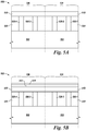
- Figures 3A-3F illustrate various process stages associated with forming array 302 of resistive memory cells in accordance with a number of embodiments of the present disclosure.
- the memory cells of array 302 can be resistive memory cells such as resistive memory cells 104, as described above.
- the array 302 can be an array of phase change memory cells.
- FIG 3A illustrates a first region 334 and a second region 336 of array 302.
- regions 334 and 336 include conductive plugs 330-1,..,330-4 formed between a heater material 310, e.g., a conductive material and a substrate 332.
- heater material 310 is limited in a direction perpendicular to the rows of memory cells (not shown) prior to a material, e.g., a resistance variable material, being formed on the heater material 310.
- the conductive plugs 330-1,...,330-4 are separated by a dielectric material 322 formed on substrate 332.
- the dielectric material 322 can be a material such as silicon dioxide or silicon nitride, for instance.
- the substrate 332 can be a silicon substrate, silicon on insulator (SOI) substrate, silicon on sapphire (SOS) substrate, for instance, and can include various doped and/or undoped semiconductor materials.
- a heater material 310 is formed on plugs 330-1,...,330-4 and can be various conductive materials, such as metal nitride, e.g., titanium nitride, tungsten nitride, among other conductive materials.
- Figure 3B illustrates a process stage subsequent to that shown in Figure 3A and associated with forming array 302.
- a resistance variable material 312-1 e.g., a phase change material, is formed on heater material 310. That is, the heater material 310 of regions 334 and 336 includes resistance variable material 312-1 formed thereon.
- a cap material 318-1 is formed on resistance variable material 312-1 in regions 334 and 336.
- Figure 3C illustrates a portion of resistance variable material 312-1 and cap material 318-1 removed from region 334 of array 302.
- the portions of materials 312-1 and 318-1 can be removed from region 334 via an etch process, for instance, without removing portions of materials 312-1 and 318-1 in region 336 of array 302.
- Figure 3D illustrates a process stage subsequent to that shown in Figure 3C and associated with forming array 302.
- Figure 3D illustrates resistance variable material 312-2 formed on heater material 310 in region 334 and cap material 318-1 in region 336 of array 302.
- Figure 3D also illustrates cap material 318-2, e.g., a conductive material, formed on resistance variable material 312-2 in regions 334 and 336.
- Figure 3E illustrates a portion of resistance variable material 312-2 and cap material 318-2 removed from region 336 of array 302.
- Removing resistance variable material 312-2 from region 336 of array 302 can result in a smooth region, including heater material 310, resistance variable material 312-1, and cap material 318-1 in region 336 of array 302.
- Region 334 of example array 302 can also be a smooth region, including heater material 310, resistance variable material 312-2, and cap material 318-2.
- cap materials 318-1 and 318-2 can serve as bit lines for the resistive memory cells.
- resistance variable materials 312-1 and 312-2 in different regions, e.g., regions 334 and 336, of an array can be used to form memory cells having different cell characteristics, e.g., electrothermal properties, within the respective array regions.
- resistance variable material 312-1 can act differently within region 336 of array 302 than 312-2 acts within region 334 of array 302.
- properties of the resistance variable materials 312-1 and 312-2 in regions 336 and 334 may be different, and resistive memory cells formed in region 334 can exhibit different cell characteristics as compared to the cell characteristics of cells formed in region 336.
- Figure 3F illustrates a process stage subsequent to that shown in Figure 3E and associated with forming array 302.
- individual resistive memory cells 313-1 and 313-2 e.g., separate cell stacks, can be defined by removing portions of materials 310, 312-1, 318-1, 312-2, and 318-2.
- resistance variable materials 312-1 and 312-2 are between two conductive elements, e.g., between a conductive cap material 318-1 and/or 318-2 and a heater material 310.
- the memory cells 313-1 and 313-2 are self-aligned and can be formed via a number of masking and etching processes, for instance.
- the array 302 can be an array of RRAM cells or other resistive memory cells having separate regions with different cell characteristics.
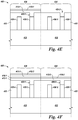
- Figures 4A-4I illustrate various process stages associated with forming an array 402 of resistive memory cells in accordance with a number of embodiments of the present disclosure.
- the memory cells of array 402 can be resistive memory cells such as resistive memory cells 104, as described above with respect to Figure 1 .
- the array 402 can be an array of phase change memory cells, but is not so limited.
- FIG 4A illustrates a first region 434 and a second region 436 of array 402.
- regions 434 and 436 of array 402 include conductive plugs 430-1,...,430-4 separated by a dielectric material 422 formed on a substrate material 432.
- the dielectric material 422 can be a material such as silicon dioxide or silicon nitride, for instance.
- the substrate 432 can be a silicon substrate, silicon on insulator (SOI) substrate, silicon on sapphire (SOS) substrate, for instance, and can include various doped and/or undoped semiconductor materials.
- Figure 4B illustrates a process stage subsequent to that shown in Figure 4A and associated with forming array 402.
- a via 420-1 is formed in a portion of rogion 436, within dielectric material 422.
- Via 420-1 can be aligned with a conductive plug in region 436, e.g., plug 430-3.
- Figure 4C illustrates a process stage subsequent to that shown in Figure 4B and associated with forming array 402.
- a resistance variable material 412-1 is formed on dielectric 422 in region 434 and region 436 of array 402. As further illustrated in Figure 4C , resistance variable material 412-1 fills via 420-1.
- a cap material 418-1 e.g., a conductive material, is formed on resistance variable material 412-1 and can comprise a number of conductive materials, including, for example, tungsten.
- Figure 4D illustrates a portion of resistance variable material 412-1 and a portion of cap material 418-1 removed from region 434 of array 402.
- the materials 412-1 and 418-1 can be removed from region 434 via an etch process, for instance, without removing materials 412-1 and 418-1 from region 436.
- Figure 4E illustrates a process stage subsequent to that shown in Figure 4D and associated with forming array 402.
- a via 420-2 is formed in a portion of region 434, within dielectric material 422.
- Via 420-2 can be aligned with a conductive plug in region 434, e.g., plug 430-1.
- Figure 4F illustrates a process stage subsequent to that shown in Figure 4E and associated with forming array 402.
- a resistance variable material 412-2 is formed on dielectric 422 in regions 434 and on cap material 418-1 in region 436 of array 402.
- resistance variable material 412- fills via 420-2.
- a cap material 418-2 is formed on resistance variable material 412-2 in regions 436 and 434 and can comprise a number of conductive materials, including, for example, tungsten.
- Figure 4G illustrates a portion of resistance variable material 412-2 and a portion of cap material 418-2 removed from region 436 of array 402.
- the materials 412-2 and 418-2 can be removed from region 436 via an etch process, for instance, without removing materials 412-2 and 418-2 from region 434.
- Figure 4H illustrates a portion of resistance variable material 412-2 and a portion of cap material 418-2 removed from region 434 of array 402 and a portion of resistance variable material 412-1 and a portion of cap material 418-1 removed from region 436 of array 402.
- Materials 412-1, 413-2, 418-1, and 418-2 can be removed from regions 434 and 436 via an etch process, such that a portion of resistance variable material 412-1 is confined to and not removed from via 420-1, and a portion of resistance variable material 412-2 is confined to and not removed from via 420-2.
- Providing different resistance variable materials, e.g., materials 412-1 and 412-2, in different regions, e.g., regions 434 and 436, of an array can be used to form memory cells having different cell characteristics, e.g., electrothermal properties, within the respective array regions.
- the performance characteristics of resistance variable material 412-1 in via 420-1 of region 436 may be different than the performance characteristics of resistance variable material 412-2 in via 420-1 of region 434.
- resistive memory cells formed in region 434 can exhibit different cell characteristics as compared to cells formed in region 436.
- Figure 4I illustrates a process stage subsequent to that shown in Figure 4H and associated with forming array 202.
- a metal material 424 e.g., a copper material, is formed on resistance variable material 412-1 and resistance variable material 412-2.
- Metal material 424 can be formed using a damascene process, and in a number of embodiments, metal material 424 can serve as a cap material, an electrode, and/or bit line.
- resistance variable material 412-1 and 412-2 are between two conductive elements, e.g., between a conductive cap material 318-1 and/or 318-2 and a conductive plug 430-1 and/or 430-2.
- metal material 424 may also interact with a separate bit line.
- a barrier material (not shown) can be formed between resistance variable materials 412-1 and 412-2 and metal material 424.
- the barrier can comprise, for example, a metal nitride, such as, for example, titanium nitride and/or tantalum nitride.
- the example shown in Figures 4A-4H is for an array of phase change memory cells, embodiments are not so limited.
- the array 402 can be an array of RRAM cells or other resistive memory cells having separate regions with different cell characteristics.
- resistance variable materials 412-1 and 412-2 can comprise phase change materials formed on the conductive plugs, e.g. plugs 430-3 and 430-1. As such, the conductive plugs can serve as heaters for array 402.
- the thermal activation can apply to a reactant material process.
Landscapes
- Engineering & Computer Science (AREA)
- Manufacturing & Machinery (AREA)
- Semiconductor Memories (AREA)
Claims (7)
- Array (102; 202) widerstandsfähiger Speicherzellen (104), mit
einer ersten Anzahl widerstandsfähiger Speicherzellen (213-1), die jeweils eine sich selbst anordnende Struktur in einer ersten Region (236; 336) des Arrays haben und ein widerstandsvariables Material (212) mit einer bestimmten damit verbundenen elektrothermischen Eigenschaft aufweisen,
einer zweiten Anzahl widerstandsfähiger Speicherzellen (213-2), die jeweils eine sich selbst anordnende Struktur in einer zweiten Region (234) des Arrays haben und ein widerstandsvariables Material (212) mit einer damit verbundenen verschiedenen elektrothermischen Eigenschaft aufweisen,
einem ersten Reaktionsmaterial (214), das auf dem widerstandsvariablen Material (212) in der ersten Region (236) des Arrays gebildet ist, und
einem zweiten Reaktionsmaterial (216), das auf dem ersten Reaktionsmaterial in der ersten Region (236) des Arrays und dem widerstandsvariablen Material (212) in der zweiten Region (234) des Arrays gebildet ist,
wobei die Dicke des auf der ersten Region (236) gebildeten ersten Reaktionsmaterials (214) verschieden ist von der Dicke des auf der zweiten Region (234) gebildeten zweiten Reaktionsmaterials (214). - Array nach Anspruch 1, wobei die erste (213-1) und die zweite (213-2) widerstandsfähige Speicherzelle an die gleiche Bitleitung (107-1, 107-2 ... 107-M) angeschlossen sind.
- Array nach Anspruch 1, wobei die erste Region (234) des Arrays eine höhere zugeordnete Speicherfähigkeit hat als die zweite Region (236; 336; 436; 536) des Arrays.
- Array nach Anspruch 1, wobei die zweite Region (236) des Arrays einen höheren zugeordneten Programmierdurchsatz aufweist als die erste Region (234) des Arrays.
- Verfahren zum Bilden eines Arrays (102; 202; 302) widerstandsfähiger Speicherzellen (104), wobei in dem Verfahren
eine erste Anzahl widerstandsfähiger Speicherzellen (213-1), die jeweils eine sich selbst anordnende Struktur in einer ersten Region (236) des Arrays aufweisen, und eine zweite Anzahl widerstandsfähiger Speicherzellen (213-2), die jeweils eine sich selbst anordnende Struktur in einer zweiten Region (234) des Arrays aufweisen, gebildet werden,
eine elektrothermische Eigenschaft eines widerstandsvariablen Materials (212) in der ersten Region (236) des Arrays und/oder der zweiten Region (234) des Arrays modifiziert wird, wobei bei dem Modifiziervorgang:ein erstes Reaktionsmaterial (214) auf dem widerstandsvariablen Material (212) in der ersten Region (236) des Arrays gebildet wird, undein zweites Reaktionsmaterial (216) auf dem ersten Reaktionsmaterial in der ersten Region (236) des Arrays und auf dem widerstandsvariablen Material (212) in der zweiten Region (234) des Arrays gebildet wird,wobei die Dicke des auf der ersten Region (236) gebildeten ersten Reaktionsmaterials (214) verschieden ist von der Dicke des auf der zweiten Region (234) gebildeten zweiten Reaktionsmaterials (214). - Verfahren nach Anspruch 5, wobei beim Modifizieren der elektrothermischen Eigenschaft des widerstandsvariablen Materials (212) in der ersten (236) und/oder zweiten (234) Region eine thermische Aktivierung durchgeführt wird, um die elektrothermischen Eigenschaften des widerstandsvariablen Materials (212) in der ersten (236) und der zweiten (234) Region des Arrays zu modifizieren.
- Verfahren nach Anspruch 5, wobei beim Modifizieren der elektrothermischen Eigenschaft des widerstandsvariablen Materials (212) in der ersten (236) und/oder zweiten (234) Region:ein Abschnitt des ersten Reaktionsmaterials (214) entfernt wird,das zweite Reaktionsmaterial (216) dort gebildet wird, wo der Abschnitt des ersten Reaktionsmaterials (214) entfernt wurde, sowie auf dem widerstandsvariablen Material (212; 512) in der ersten Region (234),ein Kappenmaterial (218) auf dem zweiten Reaktionsmaterial (216) gebildet wird, undseparate Zellenstapel entsprechend den ersten (213-1) und zweiten (213-2) widerstandsfähigen Speicherzellen gebildet werden.
Applications Claiming Priority (2)
| Application Number | Priority Date | Filing Date | Title |
|---|---|---|---|
| US13/352,680 US9318699B2 (en) | 2012-01-18 | 2012-01-18 | Resistive memory cell structures and methods |
| PCT/US2013/022189 WO2013109920A1 (en) | 2012-01-18 | 2013-01-18 | Resistive memory cell structures and methods |
Publications (3)
| Publication Number | Publication Date |
|---|---|
| EP2805351A1 EP2805351A1 (de) | 2014-11-26 |
| EP2805351A4 EP2805351A4 (de) | 2015-08-26 |
| EP2805351B1 true EP2805351B1 (de) | 2018-10-17 |
Family
ID=48779349
Family Applications (1)
| Application Number | Title | Priority Date | Filing Date |
|---|---|---|---|
| EP13739105.8A Active EP2805351B1 (de) | 2012-01-18 | 2013-01-18 | Resistive speicherzellenstrukturen und verfahren |
Country Status (5)
| Country | Link |
|---|---|
| US (5) | US9318699B2 (de) |
| EP (1) | EP2805351B1 (de) |
| KR (1) | KR101547079B1 (de) |
| CN (1) | CN104137261B (de) |
| WO (1) | WO2013109920A1 (de) |
Families Citing this family (20)
| Publication number | Priority date | Publication date | Assignee | Title |
|---|---|---|---|---|
| US9318699B2 (en) | 2012-01-18 | 2016-04-19 | Micron Technology, Inc. | Resistive memory cell structures and methods |
| US8964448B2 (en) * | 2012-08-09 | 2015-02-24 | Micron Technology, Inc. | Memory cells having a plurality of resistance variable materials |
| US9450022B1 (en) * | 2012-09-05 | 2016-09-20 | Hrl Laboratories, Llc | Memristor devices and fabrication |
| US9184377B2 (en) * | 2013-06-11 | 2015-11-10 | Micron Technology, Inc. | Resistance variable memory cell structures and methods |
| US9019754B1 (en) | 2013-12-17 | 2015-04-28 | Micron Technology, Inc. | State determination in resistance variable memory |
| US9691475B2 (en) | 2015-03-19 | 2017-06-27 | Micron Technology, Inc. | Constructions comprising stacked memory arrays |
| TWI550610B (zh) * | 2015-03-26 | 2016-09-21 | 旺宏電子股份有限公司 | 電阻式隨機存取記憶體頂電極之鑲嵌製程 |
| KR102673120B1 (ko) * | 2016-12-05 | 2024-06-05 | 삼성전자주식회사 | 반도체 장치 및 그 제조 방법 |
| US10103325B2 (en) | 2016-12-15 | 2018-10-16 | Winbond Electronics Corp. | Resistance change memory device and fabrication method thereof |
| US10157667B2 (en) | 2017-04-28 | 2018-12-18 | Micron Technology, Inc. | Mixed cross point memory |
| US10748966B2 (en) * | 2018-06-28 | 2020-08-18 | Sandisk Technologies Llc | Three-dimensional memory device containing cobalt capped copper lines and method of making the same |
| FR3084961B1 (fr) | 2018-08-08 | 2021-12-10 | Commissariat Energie Atomique | Dispositif memoire |
| FR3084963B1 (fr) * | 2018-08-08 | 2022-12-16 | Commissariat Energie Atomique | Dispositif memoire |
| KR102630031B1 (ko) * | 2018-10-05 | 2024-01-30 | 삼성전자주식회사 | 가변 저항 메모리 장치 |
| US11769046B2 (en) * | 2019-03-14 | 2023-09-26 | International Business Machines Corporation | Symmetric phase-change memory devices |
| KR102734551B1 (ko) | 2019-03-29 | 2024-11-28 | 삼성전자주식회사 | 가변 저항 메모리 장치 및 그 제조 방법 |
| CN113078258B (zh) * | 2020-01-06 | 2023-11-28 | 华邦电子股份有限公司 | 电阻式随机存取存储器及其制造方法 |
| FR3107138B1 (fr) | 2020-02-06 | 2022-02-11 | Commissariat Energie Atomique | Cellule mémoire à changement de phase |
| EP3890024B1 (de) | 2020-03-30 | 2024-05-01 | STMicroelectronics (Crolles 2) SAS | Elektronischer chip mit zwei phasenwechselspeichern und herstellungsverfahren |
| US20250048940A1 (en) * | 2023-08-01 | 2025-02-06 | Stmicroelectronics International N.V. | Process for cointegration of two phase change memory (pcm) arrays having different phase change materials, and in-memory computation system utilizing the two pcm arrays |
Family Cites Families (18)
| Publication number | Priority date | Publication date | Assignee | Title |
|---|---|---|---|---|
| US20060131555A1 (en) | 2004-12-22 | 2006-06-22 | Micron Technology, Inc. | Resistance variable devices with controllable channels |
| US7276760B2 (en) | 2005-02-25 | 2007-10-02 | Micron Technology, Inc. | Low power memory subsystem with progressive non-volatility |
| DE602005011111D1 (de) | 2005-06-03 | 2009-01-02 | St Microelectronics Srl | Selbstjustiertes Verfahren zur Herstellung von Phasenwechselspeicherzellen |
| US20070045606A1 (en) | 2005-08-30 | 2007-03-01 | Michele Magistretti | Shaping a phase change layer in a phase change memory cell |
| US7952937B2 (en) | 2006-03-16 | 2011-05-31 | Freescale Semiconductor, Inc. | Wordline driver for a non-volatile memory device, a non-volatile memory device and method |
| US8129706B2 (en) | 2006-05-05 | 2012-03-06 | Macronix International Co., Ltd. | Structures and methods of a bistable resistive random access memory |
| JP5159116B2 (ja) | 2007-02-07 | 2013-03-06 | 株式会社東芝 | 半導体記憶装置 |
| US7759237B2 (en) | 2007-06-28 | 2010-07-20 | Micron Technology, Inc. | Method of forming lutetium and lanthanum dielectric structures |
| US7663134B2 (en) | 2007-07-10 | 2010-02-16 | Taiwan Semiconductor Manufacturing Company, Ltd. | Memory array with a selector connected to multiple resistive cells |
| JP5380800B2 (ja) | 2007-07-12 | 2014-01-08 | ヤマハ株式会社 | 電子部品の製造方法 |
| JP5088036B2 (ja) | 2007-08-06 | 2012-12-05 | ソニー株式会社 | 記憶素子および記憶装置 |
| KR20090038065A (ko) | 2007-10-15 | 2009-04-20 | 주식회사 하이닉스반도체 | 상변화 메모리 장치의 제조방법 |
| US7903457B2 (en) * | 2008-08-19 | 2011-03-08 | Macronix International Co., Ltd. | Multiple phase change materials in an integrated circuit for system on a chip application |
| TW201011909A (en) | 2008-09-02 | 2010-03-16 | Sony Corp | Storage element and storage device |
| US20100308296A1 (en) | 2009-06-09 | 2010-12-09 | Agostino Pirovano | Phase change memory cell with self-aligned vertical heater |
| JP5659480B2 (ja) | 2009-10-26 | 2015-01-28 | ソニー株式会社 | 記憶装置の製造方法 |
| US9318699B2 (en) * | 2012-01-18 | 2016-04-19 | Micron Technology, Inc. | Resistive memory cell structures and methods |
| US9184377B2 (en) * | 2013-06-11 | 2015-11-10 | Micron Technology, Inc. | Resistance variable memory cell structures and methods |
-
2012
- 2012-01-18 US US13/352,680 patent/US9318699B2/en active Active
-
2013
- 2013-01-18 WO PCT/US2013/022189 patent/WO2013109920A1/en not_active Ceased
- 2013-01-18 EP EP13739105.8A patent/EP2805351B1/de active Active
- 2013-01-18 CN CN201380009237.XA patent/CN104137261B/zh active Active
- 2013-01-18 KR KR1020147022258A patent/KR101547079B1/ko active Active
-
2015
- 2015-07-08 US US14/794,162 patent/US9419056B2/en active Active
-
2016
- 2016-06-29 US US15/196,543 patent/US9935154B2/en active Active
-
2017
- 2017-12-11 US US15/836,978 patent/US10147763B2/en active Active
-
2018
- 2018-06-29 US US16/022,945 patent/US10622408B2/en active Active
Non-Patent Citations (1)
| Title |
|---|
| None * |
Also Published As
| Publication number | Publication date |
|---|---|
| US9318699B2 (en) | 2016-04-19 |
| US20160307965A1 (en) | 2016-10-20 |
| KR101547079B1 (ko) | 2015-08-24 |
| US20150333104A1 (en) | 2015-11-19 |
| US20130181183A1 (en) | 2013-07-18 |
| US20180108708A1 (en) | 2018-04-19 |
| US10147763B2 (en) | 2018-12-04 |
| US10622408B2 (en) | 2020-04-14 |
| EP2805351A4 (de) | 2015-08-26 |
| CN104137261B (zh) | 2017-03-01 |
| CN104137261A (zh) | 2014-11-05 |
| WO2013109920A1 (en) | 2013-07-25 |
| EP2805351A1 (de) | 2014-11-26 |
| US20180323238A1 (en) | 2018-11-08 |
| US9419056B2 (en) | 2016-08-16 |
| KR20140121434A (ko) | 2014-10-15 |
| US9935154B2 (en) | 2018-04-03 |
Similar Documents
| Publication | Publication Date | Title |
|---|---|---|
| EP2805351B1 (de) | Resistive speicherzellenstrukturen und verfahren | |
| JP5668141B2 (ja) | 相変化メモリ構造および方法 | |
| EP2891152B1 (de) | Auswahl von speichermatrixebenen | |
| EP2891182B1 (de) | Architektur für ein dreidimensionales speicherarray | |
| EP3309838B1 (de) | Phasenwechselspeicherzelle mit vertikalem transistor und herstellungsverfahren dafür | |
| US9343671B2 (en) | Memory cells having heaters with angled sidewalls | |
| US8283198B2 (en) | Resistive memory and methods of processing resistive memory | |
| US8716059B2 (en) | Combined conductive plug/conductive line memory arrays and methods of forming the same | |
| US9406881B1 (en) | Memory cells having a heater electrode formed between a first storage material and a second storage material and methods of forming the same | |
| WO2016003865A1 (en) | Memory cells having a first selecting chalcogenide material and a second selecting chalcogenide material and methods therof |
Legal Events
| Date | Code | Title | Description |
|---|---|---|---|
| PUAI | Public reference made under article 153(3) epc to a published international application that has entered the european phase |
Free format text: ORIGINAL CODE: 0009012 |
|
| 17P | Request for examination filed |
Effective date: 20140723 |
|
| AK | Designated contracting states |
Kind code of ref document: A1 Designated state(s): AL AT BE BG CH CY CZ DE DK EE ES FI FR GB GR HR HU IE IS IT LI LT LU LV MC MK MT NL NO PL PT RO RS SE SI SK SM TR |
|
| RIN1 | Information on inventor provided before grant (corrected) |
Inventor name: PELLIZZER, FABIO Inventor name: BEDESCHI, FERDINANDO |
|
| DAX | Request for extension of the european patent (deleted) | ||
| RA4 | Supplementary search report drawn up and despatched (corrected) |
Effective date: 20150724 |
|
| RIC1 | Information provided on ipc code assigned before grant |
Ipc: H01L 21/8247 20060101ALI20150720BHEP Ipc: H01L 27/115 20060101AFI20150720BHEP |
|
| STAA | Information on the status of an ep patent application or granted ep patent |
Free format text: STATUS: EXAMINATION IS IN PROGRESS |
|
| 17Q | First examination report despatched |
Effective date: 20161205 |
|
| REG | Reference to a national code |
Ref country code: DE Ref legal event code: R079 Ref document number: 602013045231 Country of ref document: DE Free format text: PREVIOUS MAIN CLASS: H01L0027115000 Ipc: H01L0027240000 |
|
| RIC1 | Information provided on ipc code assigned before grant |
Ipc: H01L 27/115 20060101ALI20180329BHEP Ipc: H01L 21/8246 20060101AFI20180329BHEP |
|
| GRAP | Despatch of communication of intention to grant a patent |
Free format text: ORIGINAL CODE: EPIDOSNIGR1 |
|
| STAA | Information on the status of an ep patent application or granted ep patent |
Free format text: STATUS: GRANT OF PATENT IS INTENDED |
|
| RIC1 | Information provided on ipc code assigned before grant |
Ipc: H01L 45/00 20060101ALI20180424BHEP Ipc: H01L 27/24 20060101AFI20180424BHEP |
|
| INTG | Intention to grant announced |
Effective date: 20180524 |
|
| GRAS | Grant fee paid |
Free format text: ORIGINAL CODE: EPIDOSNIGR3 |
|
| GRAA | (expected) grant |
Free format text: ORIGINAL CODE: 0009210 |
|
| STAA | Information on the status of an ep patent application or granted ep patent |
Free format text: STATUS: THE PATENT HAS BEEN GRANTED |
|
| AK | Designated contracting states |
Kind code of ref document: B1 Designated state(s): AL AT BE BG CH CY CZ DE DK EE ES FI FR GB GR HR HU IE IS IT LI LT LU LV MC MK MT NL NO PL PT RO RS SE SI SK SM TR |
|
| REG | Reference to a national code |
Ref country code: GB Ref legal event code: FG4D |
|
| REG | Reference to a national code |
Ref country code: CH Ref legal event code: EP |
|
| REG | Reference to a national code |
Ref country code: IE Ref legal event code: FG4D |
|
| REG | Reference to a national code |
Ref country code: DE Ref legal event code: R096 Ref document number: 602013045231 Country of ref document: DE Ref country code: AT Ref legal event code: REF Ref document number: 1054988 Country of ref document: AT Kind code of ref document: T Effective date: 20181115 |
|
| REG | Reference to a national code |
Ref country code: NL Ref legal event code: MP Effective date: 20181017 |
|
| REG | Reference to a national code |
Ref country code: LT Ref legal event code: MG4D |
|
| REG | Reference to a national code |
Ref country code: AT Ref legal event code: MK05 Ref document number: 1054988 Country of ref document: AT Kind code of ref document: T Effective date: 20181017 |
|
| PG25 | Lapsed in a contracting state [announced via postgrant information from national office to epo] |
Ref country code: NL Free format text: LAPSE BECAUSE OF FAILURE TO SUBMIT A TRANSLATION OF THE DESCRIPTION OR TO PAY THE FEE WITHIN THE PRESCRIBED TIME-LIMIT Effective date: 20181017 |
|
| PG25 | Lapsed in a contracting state [announced via postgrant information from national office to epo] |
Ref country code: IS Free format text: LAPSE BECAUSE OF FAILURE TO SUBMIT A TRANSLATION OF THE DESCRIPTION OR TO PAY THE FEE WITHIN THE PRESCRIBED TIME-LIMIT Effective date: 20190217 Ref country code: FI Free format text: LAPSE BECAUSE OF FAILURE TO SUBMIT A TRANSLATION OF THE DESCRIPTION OR TO PAY THE FEE WITHIN THE PRESCRIBED TIME-LIMIT Effective date: 20181017 Ref country code: HR Free format text: LAPSE BECAUSE OF FAILURE TO SUBMIT A TRANSLATION OF THE DESCRIPTION OR TO PAY THE FEE WITHIN THE PRESCRIBED TIME-LIMIT Effective date: 20181017 Ref country code: PL Free format text: LAPSE BECAUSE OF FAILURE TO SUBMIT A TRANSLATION OF THE DESCRIPTION OR TO PAY THE FEE WITHIN THE PRESCRIBED TIME-LIMIT Effective date: 20181017 Ref country code: LT Free format text: LAPSE BECAUSE OF FAILURE TO SUBMIT A TRANSLATION OF THE DESCRIPTION OR TO PAY THE FEE WITHIN THE PRESCRIBED TIME-LIMIT Effective date: 20181017 Ref country code: BG Free format text: LAPSE BECAUSE OF FAILURE TO SUBMIT A TRANSLATION OF THE DESCRIPTION OR TO PAY THE FEE WITHIN THE PRESCRIBED TIME-LIMIT Effective date: 20190117 Ref country code: ES Free format text: LAPSE BECAUSE OF FAILURE TO SUBMIT A TRANSLATION OF THE DESCRIPTION OR TO PAY THE FEE WITHIN THE PRESCRIBED TIME-LIMIT Effective date: 20181017 Ref country code: LV Free format text: LAPSE BECAUSE OF FAILURE TO SUBMIT A TRANSLATION OF THE DESCRIPTION OR TO PAY THE FEE WITHIN THE PRESCRIBED TIME-LIMIT Effective date: 20181017 Ref country code: NO Free format text: LAPSE BECAUSE OF FAILURE TO SUBMIT A TRANSLATION OF THE DESCRIPTION OR TO PAY THE FEE WITHIN THE PRESCRIBED TIME-LIMIT Effective date: 20190117 Ref country code: AT Free format text: LAPSE BECAUSE OF FAILURE TO SUBMIT A TRANSLATION OF THE DESCRIPTION OR TO PAY THE FEE WITHIN THE PRESCRIBED TIME-LIMIT Effective date: 20181017 |
|
| PG25 | Lapsed in a contracting state [announced via postgrant information from national office to epo] |
Ref country code: PT Free format text: LAPSE BECAUSE OF FAILURE TO SUBMIT A TRANSLATION OF THE DESCRIPTION OR TO PAY THE FEE WITHIN THE PRESCRIBED TIME-LIMIT Effective date: 20190217 Ref country code: AL Free format text: LAPSE BECAUSE OF FAILURE TO SUBMIT A TRANSLATION OF THE DESCRIPTION OR TO PAY THE FEE WITHIN THE PRESCRIBED TIME-LIMIT Effective date: 20181017 Ref country code: GR Free format text: LAPSE BECAUSE OF FAILURE TO SUBMIT A TRANSLATION OF THE DESCRIPTION OR TO PAY THE FEE WITHIN THE PRESCRIBED TIME-LIMIT Effective date: 20190118 Ref country code: RS Free format text: LAPSE BECAUSE OF FAILURE TO SUBMIT A TRANSLATION OF THE DESCRIPTION OR TO PAY THE FEE WITHIN THE PRESCRIBED TIME-LIMIT Effective date: 20181017 Ref country code: SE Free format text: LAPSE BECAUSE OF FAILURE TO SUBMIT A TRANSLATION OF THE DESCRIPTION OR TO PAY THE FEE WITHIN THE PRESCRIBED TIME-LIMIT Effective date: 20181017 |
|
| REG | Reference to a national code |
Ref country code: DE Ref legal event code: R097 Ref document number: 602013045231 Country of ref document: DE |
|
| PG25 | Lapsed in a contracting state [announced via postgrant information from national office to epo] |
Ref country code: CZ Free format text: LAPSE BECAUSE OF FAILURE TO SUBMIT A TRANSLATION OF THE DESCRIPTION OR TO PAY THE FEE WITHIN THE PRESCRIBED TIME-LIMIT Effective date: 20181017 Ref country code: DK Free format text: LAPSE BECAUSE OF FAILURE TO SUBMIT A TRANSLATION OF THE DESCRIPTION OR TO PAY THE FEE WITHIN THE PRESCRIBED TIME-LIMIT Effective date: 20181017 Ref country code: IT Free format text: LAPSE BECAUSE OF FAILURE TO SUBMIT A TRANSLATION OF THE DESCRIPTION OR TO PAY THE FEE WITHIN THE PRESCRIBED TIME-LIMIT Effective date: 20181017 |
|
| PLBE | No opposition filed within time limit |
Free format text: ORIGINAL CODE: 0009261 |
|
| STAA | Information on the status of an ep patent application or granted ep patent |
Free format text: STATUS: NO OPPOSITION FILED WITHIN TIME LIMIT |
|
| PG25 | Lapsed in a contracting state [announced via postgrant information from national office to epo] |
Ref country code: MC Free format text: LAPSE BECAUSE OF FAILURE TO SUBMIT A TRANSLATION OF THE DESCRIPTION OR TO PAY THE FEE WITHIN THE PRESCRIBED TIME-LIMIT Effective date: 20181017 Ref country code: RO Free format text: LAPSE BECAUSE OF FAILURE TO SUBMIT A TRANSLATION OF THE DESCRIPTION OR TO PAY THE FEE WITHIN THE PRESCRIBED TIME-LIMIT Effective date: 20181017 Ref country code: SK Free format text: LAPSE BECAUSE OF FAILURE TO SUBMIT A TRANSLATION OF THE DESCRIPTION OR TO PAY THE FEE WITHIN THE PRESCRIBED TIME-LIMIT Effective date: 20181017 Ref country code: SM Free format text: LAPSE BECAUSE OF FAILURE TO SUBMIT A TRANSLATION OF THE DESCRIPTION OR TO PAY THE FEE WITHIN THE PRESCRIBED TIME-LIMIT Effective date: 20181017 Ref country code: EE Free format text: LAPSE BECAUSE OF FAILURE TO SUBMIT A TRANSLATION OF THE DESCRIPTION OR TO PAY THE FEE WITHIN THE PRESCRIBED TIME-LIMIT Effective date: 20181017 |
|
| REG | Reference to a national code |
Ref country code: CH Ref legal event code: PL |
|
| 26N | No opposition filed |
Effective date: 20190718 |
|
| PG25 | Lapsed in a contracting state [announced via postgrant information from national office to epo] |
Ref country code: LU Free format text: LAPSE BECAUSE OF NON-PAYMENT OF DUE FEES Effective date: 20190118 |
|
| REG | Reference to a national code |
Ref country code: BE Ref legal event code: MM Effective date: 20190131 |
|
| REG | Reference to a national code |
Ref country code: IE Ref legal event code: MM4A |
|
| PG25 | Lapsed in a contracting state [announced via postgrant information from national office to epo] |
Ref country code: FR Free format text: LAPSE BECAUSE OF NON-PAYMENT OF DUE FEES Effective date: 20190131 Ref country code: SI Free format text: LAPSE BECAUSE OF FAILURE TO SUBMIT A TRANSLATION OF THE DESCRIPTION OR TO PAY THE FEE WITHIN THE PRESCRIBED TIME-LIMIT Effective date: 20181017 |
|
| PG25 | Lapsed in a contracting state [announced via postgrant information from national office to epo] |
Ref country code: BE Free format text: LAPSE BECAUSE OF NON-PAYMENT OF DUE FEES Effective date: 20190131 |
|
| PG25 | Lapsed in a contracting state [announced via postgrant information from national office to epo] |
Ref country code: CH Free format text: LAPSE BECAUSE OF NON-PAYMENT OF DUE FEES Effective date: 20190131 Ref country code: LI Free format text: LAPSE BECAUSE OF NON-PAYMENT OF DUE FEES Effective date: 20190131 |
|
| PG25 | Lapsed in a contracting state [announced via postgrant information from national office to epo] |
Ref country code: IE Free format text: LAPSE BECAUSE OF NON-PAYMENT OF DUE FEES Effective date: 20190118 |
|
| PG25 | Lapsed in a contracting state [announced via postgrant information from national office to epo] |
Ref country code: TR Free format text: LAPSE BECAUSE OF FAILURE TO SUBMIT A TRANSLATION OF THE DESCRIPTION OR TO PAY THE FEE WITHIN THE PRESCRIBED TIME-LIMIT Effective date: 20181017 |
|
| PG25 | Lapsed in a contracting state [announced via postgrant information from national office to epo] |
Ref country code: MT Free format text: LAPSE BECAUSE OF NON-PAYMENT OF DUE FEES Effective date: 20190118 |
|
| PG25 | Lapsed in a contracting state [announced via postgrant information from national office to epo] |
Ref country code: CY Free format text: LAPSE BECAUSE OF FAILURE TO SUBMIT A TRANSLATION OF THE DESCRIPTION OR TO PAY THE FEE WITHIN THE PRESCRIBED TIME-LIMIT Effective date: 20181017 |
|
| PG25 | Lapsed in a contracting state [announced via postgrant information from national office to epo] |
Ref country code: HU Free format text: LAPSE BECAUSE OF FAILURE TO SUBMIT A TRANSLATION OF THE DESCRIPTION OR TO PAY THE FEE WITHIN THE PRESCRIBED TIME-LIMIT; INVALID AB INITIO Effective date: 20130118 |
|
| PG25 | Lapsed in a contracting state [announced via postgrant information from national office to epo] |
Ref country code: MK Free format text: LAPSE BECAUSE OF FAILURE TO SUBMIT A TRANSLATION OF THE DESCRIPTION OR TO PAY THE FEE WITHIN THE PRESCRIBED TIME-LIMIT Effective date: 20181017 |
|
| REG | Reference to a national code |
Ref country code: DE Ref legal event code: R079 Ref document number: 602013045231 Country of ref document: DE Free format text: PREVIOUS MAIN CLASS: H01L0027240000 Ipc: H10B0063000000 |
|
| PGFP | Annual fee paid to national office [announced via postgrant information from national office to epo] |
Ref country code: GB Payment date: 20260126 Year of fee payment: 14 |
|
| PGFP | Annual fee paid to national office [announced via postgrant information from national office to epo] |
Ref country code: DE Payment date: 20260127 Year of fee payment: 14 |