EP2806459A1 - Substrat de gan, dispositif à semi-conducteur et procédé de fabrication de ceux-ci. - Google Patents
Substrat de gan, dispositif à semi-conducteur et procédé de fabrication de ceux-ci. Download PDFInfo
- Publication number
- EP2806459A1 EP2806459A1 EP12873311.0A EP12873311A EP2806459A1 EP 2806459 A1 EP2806459 A1 EP 2806459A1 EP 12873311 A EP12873311 A EP 12873311A EP 2806459 A1 EP2806459 A1 EP 2806459A1
- Authority
- EP
- European Patent Office
- Prior art keywords
- layer
- gan
- algan
- gan substrate
- algan layer
- Prior art date
- Legal status (The legal status is an assumption and is not a legal conclusion. Google has not performed a legal analysis and makes no representation as to the accuracy of the status listed.)
- Withdrawn
Links
Images


Classifications
-
- H—ELECTRICITY
- H10—SEMICONDUCTOR DEVICES; ELECTRIC SOLID-STATE DEVICES NOT OTHERWISE PROVIDED FOR
- H10D—INORGANIC ELECTRIC SEMICONDUCTOR DEVICES
- H10D30/00—Field-effect transistors [FET]
- H10D30/40—FETs having zero-dimensional [0D], one-dimensional [1D] or two-dimensional [2D] charge carrier gas channels
- H10D30/47—FETs having zero-dimensional [0D], one-dimensional [1D] or two-dimensional [2D] charge carrier gas channels having two-dimensional [2D] charge carrier gas channels, e.g. nanoribbon FETs or high electron mobility transistors [HEMT]
- H10D30/471—High electron mobility transistors [HEMT] or high hole mobility transistors [HHMT]
- H10D30/475—High electron mobility transistors [HEMT] or high hole mobility transistors [HHMT] having wider bandgap layer formed on top of lower bandgap active layer, e.g. undoped barrier HEMTs such as i-AlGaN/GaN HEMTs
-
- H—ELECTRICITY
- H10—SEMICONDUCTOR DEVICES; ELECTRIC SOLID-STATE DEVICES NOT OTHERWISE PROVIDED FOR
- H10D—INORGANIC ELECTRIC SEMICONDUCTOR DEVICES
- H10D30/00—Field-effect transistors [FET]
- H10D30/01—Manufacture or treatment
- H10D30/015—Manufacture or treatment of FETs having heterojunction interface channels or heterojunction gate electrodes, e.g. HEMT
-
- H—ELECTRICITY
- H10—SEMICONDUCTOR DEVICES; ELECTRIC SOLID-STATE DEVICES NOT OTHERWISE PROVIDED FOR
- H10D—INORGANIC ELECTRIC SEMICONDUCTOR DEVICES
- H10D62/00—Semiconductor bodies, or regions thereof, of devices having potential barriers
- H10D62/10—Shapes, relative sizes or dispositions of the regions of the semiconductor bodies; Shapes of the semiconductor bodies
- H10D62/102—Constructional design considerations for preventing surface leakage or controlling electric field concentration
- H10D62/103—Constructional design considerations for preventing surface leakage or controlling electric field concentration for increasing or controlling the breakdown voltage of reverse-biased devices
- H10D62/105—Constructional design considerations for preventing surface leakage or controlling electric field concentration for increasing or controlling the breakdown voltage of reverse-biased devices by having particular doping profiles, shapes or arrangements of PN junctions; by having supplementary regions, e.g. junction termination extension [JTE]
- H10D62/106—Constructional design considerations for preventing surface leakage or controlling electric field concentration for increasing or controlling the breakdown voltage of reverse-biased devices by having particular doping profiles, shapes or arrangements of PN junctions; by having supplementary regions, e.g. junction termination extension [JTE] having supplementary regions doped oppositely to or in rectifying contact with regions of the semiconductor bodies, e.g. guard rings with PN or Schottky junctions
-
- H—ELECTRICITY
- H10—SEMICONDUCTOR DEVICES; ELECTRIC SOLID-STATE DEVICES NOT OTHERWISE PROVIDED FOR
- H10D—INORGANIC ELECTRIC SEMICONDUCTOR DEVICES
- H10D62/00—Semiconductor bodies, or regions thereof, of devices having potential barriers
- H10D62/80—Semiconductor bodies, or regions thereof, of devices having potential barriers characterised by the materials
- H10D62/82—Heterojunctions
- H10D62/824—Heterojunctions comprising only Group III-V materials heterojunctions, e.g. GaN/AlGaN heterojunctions
-
- H—ELECTRICITY
- H10—SEMICONDUCTOR DEVICES; ELECTRIC SOLID-STATE DEVICES NOT OTHERWISE PROVIDED FOR
- H10D—INORGANIC ELECTRIC SEMICONDUCTOR DEVICES
- H10D62/00—Semiconductor bodies, or regions thereof, of devices having potential barriers
- H10D62/80—Semiconductor bodies, or regions thereof, of devices having potential barriers characterised by the materials
- H10D62/85—Semiconductor bodies, or regions thereof, of devices having potential barriers characterised by the materials being Group III-V materials, e.g. GaAs
- H10D62/8503—Nitride Group III-V materials, e.g. AlN or GaN
-
- H—ELECTRICITY
- H10—SEMICONDUCTOR DEVICES; ELECTRIC SOLID-STATE DEVICES NOT OTHERWISE PROVIDED FOR
- H10P—GENERIC PROCESSES OR APPARATUS FOR THE MANUFACTURE OR TREATMENT OF DEVICES COVERED BY CLASS H10
- H10P14/00—Formation of materials, e.g. in the shape of layers or pillars
- H10P14/20—Formation of materials, e.g. in the shape of layers or pillars of semiconductor materials
- H10P14/24—Formation of materials, e.g. in the shape of layers or pillars of semiconductor materials using chemical vapour deposition [CVD]
-
- H—ELECTRICITY
- H10—SEMICONDUCTOR DEVICES; ELECTRIC SOLID-STATE DEVICES NOT OTHERWISE PROVIDED FOR
- H10P—GENERIC PROCESSES OR APPARATUS FOR THE MANUFACTURE OR TREATMENT OF DEVICES COVERED BY CLASS H10
- H10P14/00—Formation of materials, e.g. in the shape of layers or pillars
- H10P14/20—Formation of materials, e.g. in the shape of layers or pillars of semiconductor materials
- H10P14/29—Formation of materials, e.g. in the shape of layers or pillars of semiconductor materials characterised by the substrates
- H10P14/2901—Materials
-
- H—ELECTRICITY
- H10—SEMICONDUCTOR DEVICES; ELECTRIC SOLID-STATE DEVICES NOT OTHERWISE PROVIDED FOR
- H10P—GENERIC PROCESSES OR APPARATUS FOR THE MANUFACTURE OR TREATMENT OF DEVICES COVERED BY CLASS H10
- H10P14/00—Formation of materials, e.g. in the shape of layers or pillars
- H10P14/20—Formation of materials, e.g. in the shape of layers or pillars of semiconductor materials
- H10P14/29—Formation of materials, e.g. in the shape of layers or pillars of semiconductor materials characterised by the substrates
- H10P14/2901—Materials
- H10P14/2907—Materials being Group IIIA-VA materials
- H10P14/2908—Nitrides
-
- H—ELECTRICITY
- H10—SEMICONDUCTOR DEVICES; ELECTRIC SOLID-STATE DEVICES NOT OTHERWISE PROVIDED FOR
- H10P—GENERIC PROCESSES OR APPARATUS FOR THE MANUFACTURE OR TREATMENT OF DEVICES COVERED BY CLASS H10
- H10P14/00—Formation of materials, e.g. in the shape of layers or pillars
- H10P14/20—Formation of materials, e.g. in the shape of layers or pillars of semiconductor materials
- H10P14/32—Formation of materials, e.g. in the shape of layers or pillars of semiconductor materials characterised by intermediate layers between substrates and deposited layers
- H10P14/3202—Materials thereof
- H10P14/3214—Materials thereof being Group IIIA-VA semiconductors
- H10P14/3216—Nitrides
-
- H—ELECTRICITY
- H10—SEMICONDUCTOR DEVICES; ELECTRIC SOLID-STATE DEVICES NOT OTHERWISE PROVIDED FOR
- H10P—GENERIC PROCESSES OR APPARATUS FOR THE MANUFACTURE OR TREATMENT OF DEVICES COVERED BY CLASS H10
- H10P14/00—Formation of materials, e.g. in the shape of layers or pillars
- H10P14/20—Formation of materials, e.g. in the shape of layers or pillars of semiconductor materials
- H10P14/34—Deposited materials, e.g. layers
- H10P14/3402—Deposited materials, e.g. layers characterised by the chemical composition
- H10P14/3414—Deposited materials, e.g. layers characterised by the chemical composition being group IIIA-VIA materials
- H10P14/3416—Nitrides
-
- H—ELECTRICITY
- H10—SEMICONDUCTOR DEVICES; ELECTRIC SOLID-STATE DEVICES NOT OTHERWISE PROVIDED FOR
- H10P—GENERIC PROCESSES OR APPARATUS FOR THE MANUFACTURE OR TREATMENT OF DEVICES COVERED BY CLASS H10
- H10P14/00—Formation of materials, e.g. in the shape of layers or pillars
- H10P14/20—Formation of materials, e.g. in the shape of layers or pillars of semiconductor materials
- H10P14/34—Deposited materials, e.g. layers
- H10P14/3438—Doping during depositing
- H10P14/3441—Conductivity type
- H10P14/3444—P-type
-
- H—ELECTRICITY
- H10—SEMICONDUCTOR DEVICES; ELECTRIC SOLID-STATE DEVICES NOT OTHERWISE PROVIDED FOR
- H10P—GENERIC PROCESSES OR APPARATUS FOR THE MANUFACTURE OR TREATMENT OF DEVICES COVERED BY CLASS H10
- H10P14/00—Formation of materials, e.g. in the shape of layers or pillars
- H10P14/20—Formation of materials, e.g. in the shape of layers or pillars of semiconductor materials
- H10P14/38—Formation of materials, e.g. in the shape of layers or pillars of semiconductor materials characterised by treatments done after the formation of the materials
Definitions
- the present invention relates to a microelectronic technology, and in particular, to a GaN substrate, a semiconductor device and methods for fabricating a GaN substrate and a semiconductor device.
- Gallium nitride a third generation wide bandgap semiconductor material, draws much attention because of its characteristics of wide bandgap, high breakdown voltage, high saturation electron velocity and the like.
- a Si-based LDMOS Lateral Double-Diffused Metal-Oxide Semiconductor, lateral double-diffused metal-oxide semiconductor
- GaN HEMT High Electron Mobility Transistor, high electron mobility transistor
- the GaN HEMT device frequently generates a current collapse effect, which may causes decrease of direct drain currents, gains and radio frequency output power of the GaN HEMT device. How to reduce the current collapse effect becomes a problem that needs to be solved urgently.
- Embodiments of the present invention provide a GaN substrate, a semiconductor device and methods for fabricating a GaN substrate and a semiconductor device, so as to reduce a collapse effect of the semiconductor device caused by the GaN substrate.
- a first aspect of the embodiments of the present invention provides a GaN substrate, including:
- Another aspect of the embodiments of the present invention provides a semiconductor device, including the GaN substrate and a semiconductor structure formed on the GaN substrate.
- Still another aspect of the embodiments of the present invention provides a method for fabricating a GaN substrate, including:
- Yet another aspect of the embodiments of the present invention provides a method for fabricating a semiconductor device, including:
- a p-type conducting layer is formed on an AlGaN layer, and a hole charge carrier on the p-type conducting layer can be used to exhaust surface state negative electrons on an n-type AlGaN layer, neutralize a dangling bond on a section of the AlGaN layer, and prevent the forming of a virtual gate, so as to suppress a current collapse effect of the semiconductor device fabricated using the GaN substrate, thereby improving performance of the semiconductor device, and enhancing reliability of the semiconductor device.
- This embodiment provides a method for fabricating a GaN substrate.
- FIG. 1 is a schematic flowchart of the method for fabricating a GaN substrate according to this embodiment. Specific steps are as follows:
- the semiconductor base may be a GaN base of any type, and preferably, a composite base whose surface layer is a GaN layer.
- the GaN base includes a base layer and a GaN layer that are formed sequentially, where the base layer may be made of SiC, sapphire, or Si.
- Step 102 Form a p-type conducting layer on an active area of the AlGaN layer, where the p-type conducting layer is used to exhaust surface state negative electrons on the AlGaN layer and neutralize a dangling bond on the AlGaN layer.
- the active area of the AlGaN layer is an area where a gate electrode, a source electrode, and a drain electrode are to be formed, and/or an area between the electrodes.
- an area other than the active area is covered with photoresist, then the p-type conducting layer is formed on the active area, and the photoresist and the p-type conducting layer outside the active area are removed.
- the p-type conducting layer is formed on the AlGaN layer, then a layer of photoresist is formed on the active area, the p-type conducting layer outside the active area is removed, and finally the photoresist is removed.
- a specific forming manner may be selected according to a practical requirement, which will not be described herein.
- a p-type conducting layer is formed on an AlGaN layer, and a hole charge carrier in the p-type conducting layer can be used to exhaust surface state negative electrons on the n-type AlGaN layer, neutralize a dangling bond on a section of the AlGaN layer, and prevent the forming of a virtual gate, so as to suppress a current collapse effect of a semiconductor device fabricated using the GaN substrate, thereby improving performance of the semiconductor device, and enhancing reliability of the semiconductor device.
- This embodiment provides a method for forming a GaN substrate.
- FIG. 2 is a schematic flowchart of the method for forming a GaN substrate according to this embodiment.
- a material of the base layer may be SiC, sapphire, or Si.
- a SiC layer is used in this embodiment.
- an MOCVD Metal-organic Chemical Vapor Deposition, metal-organic chemical vapor deposition
- MOCVD Metal-organic Chemical Vapor Deposition, metal-organic chemical vapor deposition
- TMGa trimethyl gallium
- NH 3 ammonia gas
- thickness of the GaN layer may be 1 to 2 ⁇ m.
- the GaN layer is an undoped GaN layer.
- Thickness of the AlGaN layer may be 25 nm to 35 nm
- a specific forming method may be growing the AlGaN layer on the GaN layer at a temperature of around 1100°C by using the MOCVD method, where TMGa, TMA1 (trimethylaluminum) and NH 3 may be used as source gases, and preferably, the AlGaN layer is an undoped AlGaN layer.
- a p-type GaN layer is formed on the photoresist layer with the pattern, where the p-type GaN layer may be a GaN layer doped with Be, a GaN layer doped with Zn, or a GaN layer doped with Mg.
- a forming method is as follows:
- a buffer layer may be grown between step 201 and step 202.
- the buffer layer may be formed by AlN.
- the buffer layer is grown by using the MOCVD method at a temperature of around 1100°C.
- TMA1 and NH 3 may be used as source gases, and thickness of the buffer layer may be 10 to 200 nm, and preferably, 10 nm.
- a function of the buffer layer AlN is that the GaN layer and the SiC layer have large lattice mismatch, resulting in poor adhesivity; therefore, the AlN layer can reduce defect density resulting from stress mismatch which is caused by the lattice mismatch and increase adhesivity between GaN and SiC, and AlN has buffering and transition functions.
- a p-type GaN layer is formed on an AlGaN layer, and a hole charge carrier in the p-type GaN layer can be used to exhaust surface state negative electrons on the n-type AlGaN layer, neutralize a dangling bond on a section of the AlGaN layer, and prevent the forming of a virtual gate, so as to suppress a current collapse effect of a semiconductor device fabricated using the GaN substrate, thereby improving performance of the semiconductor device and enhancing reliability of the semiconductor device.
- This embodiment provides a method for fabricating a semiconductor device.
- the semiconductor device is fabricated using the GaN substrate formed in Embodiment 1 or Embodiment 2 as a substrate.
- Forming a GaN layer doped with Mg on AlGaN is used as an example for description in the following.
- a material of the base layer may be SiC, sapphire, or Si.
- an MOCVD Metal-organic Chemical Vapor Deposition, metal-organic chemical vapor deposition
- MOCVD Metal-organic Chemical Vapor Deposition, metal-organic chemical vapor deposition
- TMGa trimethyl gallium
- NH 3 ammonia gas
- thickness of the GaN layer may be 1 to 2 ⁇ m.
- the GaN layer is an undoped GaN layer.
- Step 301 and step 302 are steps that form a GaN base.
- Thickness of the AlGaN layer may be 25 nm to 35 nm
- a specific forming method may be growing the AlGaN layer on the GaN layer at a temperature of around 1100°C by using the MOCVD method, where TMGa, TMA1 (trimethylaluminum) and NH 3 may be used as source gases, and preferably, the AlGaN layer is an undoped AlGaN layer.
- Step 304 may specifically be forming a layer of photoresist on the AlGaN layer, and performing an exposure operation on the photoresist, so as to form a photoresist layer with a pattern, that is, the active area is not covered with the photoresist, and the other area is covered with the photoresist.
- a forming method is as follows:
- a GaN layer of 8 to 12 nm thick and doped with Mg is grown on AlGaN with a gas mixture of NH 3 , TMGa, and Cp 2 Mg as a source gas; H 2 as a carrier gas; a reaction pressure of 2 to 3 Pa; and a growth temperature of 900 to 1100°C. Then, annealing treatment is performed on the GaN layer doped with Mg in an N 2 atmosphere of 700 to 800°C, where an annealing duration is 20 to 30 minutes, so as to form a final p-type conducting GaN layer. This method can obtain a hole density of 10 17 to 10 18 cm -3 .
- the hole density is high; therefore, surface state negative electrons on the AlGaN layer can be effectively exhausted and a dangling bond on a section of the AlGaN layer can be effectively neutralized.
- this method does not need addition of a new deposition device, that is, no excessive cost is required.
- the n-type AlGaN and the p-type GaN doped with Mg have small lattice thermal mismatch, which is conducive to improving performance of the whole GaN substrate.
- a buffer layer may be grown between step 301 and step 302.
- the buffer layer may be formed by AlN.
- the buffer layer is grown by using the MOCVD method at a temperature of around 1100°C.
- TMA1 and NH 3 may be used as source gases, and thickness of the buffer layer may be 10 to 200 nm, and preferably, 10 nm.
- a source electrode and a drain electrode are formed on the GaN substrate.
- a photolithography technology is adopted, and photoresist is used to cover an area other than the area where the source electrode and the drain electrode are formed.
- an isolation operation is performed on the active area.
- an ion implantation method may be used to form an isolation area, for example, implanting B ions.
- a specific operation is described in the prior art, and will not be repeated herein.
- a gate electrode is formed on the GaN substrate.
- the photolithography technology is adopted, the photoresist is used to cover an area other than a preset area where the gate electrode is formed, the p-type GaN layer where the gate electrode 601 is located is removed by etching, and Ni of around 50 nm and Au of around 500 nm are sequentially evaporated.
- the photoresist and an undesired Ni/Au film layer are removed by using an etching technology, so as to form the gate electrode constituted by Ni/Au.
- annealing treatment is performed, for example, thermal processing is performed for 2 to 3 minutes under a condition of around 700°C, so as to form ideal Schottky contact with the GaN substrate.
- the forming the semiconductor structure in this step may further include forming a metal interconnection layer on the GaN substrate where the gate electrode, the source electrode and the drain electrode are formed, where the metal interconnection layer may be formed on the source electrode and the drain electrode.
- metal interconnection layers formed by various metal interconnection processes are already available, which will not be described herein again.
- a PECVD method may be further used to deposit a SiN passivation layer.
- the SiN passivation layer can be used for protection, for example, absorbing moisture in the air that enters the semiconductor device, so as to avoid affecting conductivity of the source electrode and the drain electrode and improve reliability of the semiconductor device with a GaN substrate.
- a p-type GaN layer is formed on an AlGaN layer, and a hole charge carrier in the p-type GaN layer can exhaust surface state negative electrons on the n-type AlGaN layer, neutralize a dangling bond on a section of the AlGaN layer, and prevent the forming of a virtual gate, so as to suppress a current collapse effect of the semiconductor device according to this embodiment, thereby improving performance of the semiconductor device, and enhancing reliability of the semiconductor device.
- This embodiment provides a GaN substrate.
- FIG. 3 is a schematic structural diagram of a GaN substrate according to this embodiment.
- the GaN substrate includes a GaN base 401, an AlGaN layer 402, and a p-type conducting layer 403.
- the GaN base may be a GaN base of any type, and preferably, a composite substrate whose surface layer is a GaN layer.
- the GaN base includes a base layer and a GaN layer that are formed sequentially, where the base layer may be made of SiC, sapphire, or Si.
- the AlGaN layer 402 is disposed on the GaN base 401.
- the p-type conducting layer 403 is disposed on an active area of the AlGaN layer 402, and is used to exhaust surface state negative electrons on the AlGaN layer 402 and neutralize a dangling bond on the AlGaN layer 402.
- a specific method for fabricating the GaN substrate is similar to the foregoing embodiments, and is not repeated herein.
- the p-type conducting layer 403 is formed on the AlGaN layer 402, and a hole charge carrier in the p-type conducting layer 403 can be used to exhaust surface state negative electrons on the n-type AlGaN layer 402, neutralize a dangling bond on a section of the AlGaN layer 402, and prevent the forming of a virtual gate, so as to suppress a current collapse effect of a semiconductor device fabricated using the GaN substrate, thereby improving performance of the semiconductor device, and enhancing reliability of the semiconductor device.
- This embodiment provides a specific GaN substrate based on Embodiment 4.
- FIG. 4 is a schematic structural diagram of a GaN substrate according to this embodiment.
- the GaN substrate specifically includes a base layer 501, a GaN layer 502, the AlGaN layer 402, and the p-type GaN layer 403 that are formed sequentially.
- the base layer 501 and the GaN layer 502 form the GaN base 401.
- the base layer 501 in this embodiment adopts SiC.
- the GaN layer 502 may be formed by using an MOCVD (Metal-organic Chemical Vapor Deposition, metal-organic chemical vapor deposition) method at a temperature of around 900°C, where TMGa (trimethyl gallium) and NH 3 (ammonia gas) may be used as source gases, and thickness of the GaN layer 502 may be 1 to 2 ⁇ m.
- MOCVD Metal-organic Chemical Vapor Deposition, metal-organic chemical vapor deposition
- TMGa trimethyl gallium
- NH 3 ammonia gas
- the GaN layer 502 is an undoped GaN layer.
- Thickness of the AlGaN layer 402 may be 25 nm to 35 nm
- a specific forming method may be growing the AlGaN layer 402 on the GaN layer at a temperature of around 1100°C by using the MOCVD method, where TMGa, TMA1 (trimethylaluminum) and NH 3 may be used as source gases, and preferably, the AlGaN layer 402 is an undoped AlGaN layer.
- the p-type GaN layer 403 may specifically be a GaN layer doped with Be, a GaN layer doped with Zn, or a GaN layer doped with Mg.
- a forming method is as follows:
- a buffer layer 503 may be grown between the base layer 501 and the GaN layer 502.
- the buffer layer 503 may be an AlN layer.
- the buffer layer 503 is grown by using the MOCVD method at a temperature of around 1100°C. TMA1 and NH 3 may be used as source gases, and thickness of the buffer layer 503 may be 10 to 200 nm, and preferably, 10 nm.
- a function of the buffer layer is that the GaN layer and the SiC layer have large lattice mismatch, resulting in poor adhesivity; therefore, the AlN layer 503 can reduce defect density resulting from stress mismatch which is caused by the lattice mismatch and increase adhesivity between GaN and SiC, and the AlN layer 503 has buffering and transition functions.
- the p-type GaN layer 403 is formed on the AlGaN layer 402, and a hole charge carrier in the p-type GaN layer 403 can be used to exhaust surface state negative electrons on the n-type AlGaN layer 402, neutralize a dangling bond on a section of the AlGaN layer 402, and prevent the forming of a virtual gate, so as to suppress a current collapse effect of a semiconductor device fabricated using the GaN substrate, thereby improving performance of the semiconductor device, and enhancing reliability of the semiconductor device.
- This embodiment provides a semiconductor device, and a specific forming method is described in Embodiment 3.
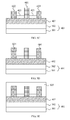
- FIG. 5A to FIG. 5E are schematic structural diagrams of a semiconductor device according to this embodiment.
- the semiconductor device includes the semiconductor substrate described in Embodiment 4 or Embodiment 5.
- FIG. 5A to FIG. 5E each show a structure of the semiconductor substrate described in Embodiment 5, and a specific structure and a forming manner of the semiconductor substrate are consistent with that in the foregoing embodiments, which will not be described herein again.
- a semiconductor structure is further provided on the semiconductor substrate, and the semiconductor structure specifically includes a gate electrode 601, a source electrode 602, and a drain electrode 603, and may further include a metal interconnection layer 604 and/or a SiN passivation layer 605.
- a forming manner of the semiconductor structure is specifically as follows:
- the source electrode 602 and the drain electrode 603 are formed on a GaN substrate.
- a photolithography technology is adopted, and photoresist 701 is used to cover an area other than the area where the source electrode 602 and the drain electrode 603 are formed.
- the photoresist and metal Ti/Al/Ti/Au in a non-active area are removed by using an etching method. As shown in FIG. 5B , in this way, the source electrode 602 and the drain electrode 603 constituted by the composite metal layer Ti/Al/Ti/Au are formed.
- an isolation operation is performed on an active area (not shown).
- an ion implantation method may be used to form an isolation area, for example, implanting B ions.
- a specific operation is described in the prior art, and will not be repeated herein.
- the gate electrode 601 is formed on the GaN substrate.
- the photolithography technology is adopted, the photoresist is used to cover an area other than a preset area where the gate electrode 601 is formed, and the p-type GaN layer 403 where the gate electrode 601 is located is removed by etching.
- Ni of around 50 nm and Au of around 500 nm are sequentially evaporated.
- the photoresist and an undesired Ni/Au film layer are removed by using an etching technology, so as to form the gate electrode 601 constituted by Ni/Au shown in FIG. 5C .
- annealing treatment is performed, for example, thermal processing is performed for 2 to 3 minutes under a condition of around 700°C, so as to form ideal Schottky contact between the gate electrode 601 and the GaN substrate.
- the metal interconnection layer 604 is formed on the GaN substrate where the gate electrode 601, the source electrode 602 and the drain electrode 603 are formed, and the metal interconnection layer 604 may be formed on the source electrode 602 and the drain electrode 603.
- metal interconnection layers formed by various metal interconnection processes are already available, which will not be described herein again.
- a PECVD method may be further used to deposit the SiN passivation layer 605.
- the SiN passivation layer 605 can be used for protection, for example, absorbing moisture in the air that enters the semiconductor device, so as to avoid affecting conductivity of the source electrode 602 and the drain electrode 603, and improve reliability of the semiconductor device with a GaN substrate.
- the forming the semiconductor structure in this step may further include forming a metal interconnection layer (not shown) after the SiN passivation layer is formed.
- a metal interconnection layer (not shown) after the SiN passivation layer is formed.
- the p-type GaN layer 403 is formed on the AlGaN layer 402, and a hole charge carrier in the p-type GaN layer 403 can be used to exhaust surface state negative electrons on the n-type AlGaN layer 402, neutralize a dangling bond on a section of the AlGaN layer 402, and prevent the forming of a virtual gate, so as to suppress a current collapse effect of the semiconductor device according to this embodiment, thereby improving performance of the semiconductor device, and enhancing reliability of the semiconductor device.
Landscapes
- Junction Field-Effect Transistors (AREA)
- Chemical & Material Sciences (AREA)
- Engineering & Computer Science (AREA)
- Materials Engineering (AREA)
Applications Claiming Priority (2)
| Application Number | Priority Date | Filing Date | Title |
|---|---|---|---|
| CN2012100862945A CN102637723A (zh) | 2012-03-28 | 2012-03-28 | GaN衬底、半导体器件及其制作方法 |
| PCT/CN2012/084300 WO2013143289A1 (fr) | 2012-03-28 | 2012-11-08 | Substrat de gan, dispositif à semi-conducteur et procédé de fabrication de ceux-ci. |
Publications (2)
| Publication Number | Publication Date |
|---|---|
| EP2806459A1 true EP2806459A1 (fr) | 2014-11-26 |
| EP2806459A4 EP2806459A4 (fr) | 2015-02-25 |
Family
ID=46622047
Family Applications (1)
| Application Number | Title | Priority Date | Filing Date |
|---|---|---|---|
| EP12873311.0A Withdrawn EP2806459A4 (fr) | 2012-03-28 | 2012-11-08 | Substrat de gan, dispositif à semi-conducteur et procédé de fabrication de ceux-ci. |
Country Status (4)
| Country | Link |
|---|---|
| US (1) | US9653588B2 (fr) |
| EP (1) | EP2806459A4 (fr) |
| CN (1) | CN102637723A (fr) |
| WO (1) | WO2013143289A1 (fr) |
Cited By (1)
| Publication number | Priority date | Publication date | Assignee | Title |
|---|---|---|---|---|
| EP2881982B1 (fr) * | 2013-12-05 | 2019-09-04 | IMEC vzw | Procédé de fabrication de couches de contact compatibles CMOS dans des dispositifs à semi-conducteurs |
Families Citing this family (5)
| Publication number | Priority date | Publication date | Assignee | Title |
|---|---|---|---|---|
| CN102637723A (zh) * | 2012-03-28 | 2012-08-15 | 华为技术有限公司 | GaN衬底、半导体器件及其制作方法 |
| US11393806B2 (en) | 2019-09-23 | 2022-07-19 | Analog Devices, Inc. | Gallium nitride and silicon carbide hybrid power device |
| EP3926689B1 (fr) | 2020-04-20 | 2023-03-01 | Huawei Technologies Co., Ltd. | Dispositif au nitrure de gallium et son circuit de pilotage |
| US20220376041A1 (en) * | 2021-04-12 | 2022-11-24 | Innoscience (Suzhou) Technology Co., Ltd. | Semiconductor device and method for manufacturing the same |
| CN115632061B (zh) * | 2022-06-28 | 2025-08-19 | 江苏镓宏半导体有限公司 | 一种GaN基HEMT外延结构及其制备方法 |
Family Cites Families (13)
| Publication number | Priority date | Publication date | Assignee | Title |
|---|---|---|---|---|
| JP4744109B2 (ja) * | 2004-07-20 | 2011-08-10 | トヨタ自動車株式会社 | 半導体装置とその製造方法 |
| JP2007220895A (ja) | 2006-02-16 | 2007-08-30 | Matsushita Electric Ind Co Ltd | 窒化物半導体装置およびその製造方法 |
| JP2007329350A (ja) * | 2006-06-08 | 2007-12-20 | Matsushita Electric Ind Co Ltd | 半導体装置 |
| JP5186096B2 (ja) * | 2006-10-12 | 2013-04-17 | パナソニック株式会社 | 窒化物半導体トランジスタ及びその製造方法 |
| EP2221855A4 (fr) * | 2007-11-21 | 2013-08-07 | Mitsubishi Chem Corp | Semi-conducteur au nitrure et procédé de croissance de cristal de semi-conducteur au nitrure |
| JP5218117B2 (ja) | 2008-03-18 | 2013-06-26 | 三菱電機株式会社 | 窒化物半導体積層構造及び光半導体装置並びにその製造方法 |
| WO2010118087A1 (fr) * | 2009-04-08 | 2010-10-14 | Efficient Power Conversion Corporation | Transistor à haute mobilité d'électrons (hemt) au gan à mode d'enrichissement et son procédé de fabrication |
| DE112010001556B4 (de) * | 2009-04-08 | 2022-01-27 | Efficient Power Conversion Corporation | Rückdiffusionsunterdrückende Strukturen |
| DE102009041548A1 (de) * | 2009-09-15 | 2011-03-24 | Fraunhofer-Gesellschaft zur Förderung der angewandten Forschung e.V. | Halbleiterstruktur |
| JP5620767B2 (ja) * | 2010-09-17 | 2014-11-05 | パナソニック株式会社 | 半導体装置 |
| JP5775321B2 (ja) * | 2011-02-17 | 2015-09-09 | トランスフォーム・ジャパン株式会社 | 半導体装置及びその製造方法、電源装置 |
| JP5784440B2 (ja) * | 2011-09-28 | 2015-09-24 | トランスフォーム・ジャパン株式会社 | 半導体装置の製造方法及び半導体装置 |
| CN102637723A (zh) * | 2012-03-28 | 2012-08-15 | 华为技术有限公司 | GaN衬底、半导体器件及其制作方法 |
-
2012
- 2012-03-28 CN CN2012100862945A patent/CN102637723A/zh active Pending
- 2012-11-08 WO PCT/CN2012/084300 patent/WO2013143289A1/fr not_active Ceased
- 2012-11-08 EP EP12873311.0A patent/EP2806459A4/fr not_active Withdrawn
-
2014
- 2014-08-22 US US14/466,295 patent/US9653588B2/en active Active
Cited By (1)
| Publication number | Priority date | Publication date | Assignee | Title |
|---|---|---|---|---|
| EP2881982B1 (fr) * | 2013-12-05 | 2019-09-04 | IMEC vzw | Procédé de fabrication de couches de contact compatibles CMOS dans des dispositifs à semi-conducteurs |
Also Published As
| Publication number | Publication date |
|---|---|
| CN102637723A (zh) | 2012-08-15 |
| WO2013143289A1 (fr) | 2013-10-03 |
| US20140361311A1 (en) | 2014-12-11 |
| US9653588B2 (en) | 2017-05-16 |
| EP2806459A4 (fr) | 2015-02-25 |
Similar Documents
| Publication | Publication Date | Title |
|---|---|---|
| CN107946358B (zh) | 一种与Si-CMOS工艺兼容的AlGaN/GaN异质结HEMT器件及其制作方法 | |
| US8912570B2 (en) | High electron mobility transistor and method of forming the same | |
| US20090189191A1 (en) | Semiconductor device | |
| CN111900203B (zh) | 一种GaN基高空穴迁移率晶体管及其制备方法 | |
| US20140091364A1 (en) | Compound semiconductor device and method of manufacturing the same | |
| US9653588B2 (en) | GaN substrate, semiconductor device and method for fabricating GaN substrate and semiconductor device | |
| US20130240901A1 (en) | Nitride semiconductor device | |
| JP5566670B2 (ja) | GaN系電界効果トランジスタ | |
| JP6882503B2 (ja) | 高ブレークダウン電圧の窒化ガリウム系高電子移動度トランジスタおよびその形成方法 | |
| US8698202B2 (en) | Semiconductor device | |
| CN109873034B (zh) | 沉积多晶AlN的常关型HEMT功率器件及其制备方法 | |
| JP2013098440A (ja) | 化合物半導体装置及びその製造方法 | |
| EP2575177A2 (fr) | Procédé de fabrication dýun dispositif semi-conducteur de composé | |
| CN113380623A (zh) | 通过p型钝化实现增强型HEMT的方法 | |
| JP2009010107A (ja) | 半導体装置及びその製造方法 | |
| US10784367B2 (en) | Semiconductor device and semiconductor device manufacturing method | |
| CN110299407A (zh) | 功率器件及其制备方法 | |
| CN108417627A (zh) | 一种用于制备GaN基高频微波器件的方法 | |
| CN111446296B (zh) | p型栅增强型氮化镓基高迁移率晶体管结构及制作方法 | |
| CN112054056A (zh) | 具有栅极静电防护结构的高电子迁移率晶体管及制作方法 | |
| CN104201199B (zh) | 增强型半导体器件和半导体集成电路装置 | |
| CN113725297B (zh) | 一种具有盖帽层的常开型氧化镓基hfet器件及其制备方法 | |
| CN212182338U (zh) | 半导体结构 | |
| JP5509544B2 (ja) | 半導体装置及びその製造方法 | |
| JP2006059956A (ja) | 半導体装置の製造方法 |
Legal Events
| Date | Code | Title | Description |
|---|---|---|---|
| PUAI | Public reference made under article 153(3) epc to a published international application that has entered the european phase |
Free format text: ORIGINAL CODE: 0009012 |
|
| 17P | Request for examination filed |
Effective date: 20140820 |
|
| AK | Designated contracting states |
Kind code of ref document: A1 Designated state(s): AL AT BE BG CH CY CZ DE DK EE ES FI FR GB GR HR HU IE IS IT LI LT LU LV MC MK MT NL NO PL PT RO RS SE SI SK SM TR |
|
| A4 | Supplementary search report drawn up and despatched |
Effective date: 20150127 |
|
| RIC1 | Information provided on ipc code assigned before grant |
Ipc: H01L 29/20 20060101ALN20150121BHEP Ipc: H01L 29/06 20060101ALI20150121BHEP Ipc: H01L 21/338 20060101ALI20150121BHEP Ipc: H01L 29/778 20060101AFI20150121BHEP Ipc: H01L 21/20 20060101ALI20150121BHEP |
|
| DAX | Request for extension of the european patent (deleted) | ||
| 17Q | First examination report despatched |
Effective date: 20160422 |
|
| STAA | Information on the status of an ep patent application or granted ep patent |
Free format text: STATUS: THE APPLICATION HAS BEEN WITHDRAWN |
|
| 18W | Application withdrawn |
Effective date: 20190909 |