EP2806474A2 - Filling film and method of manufacturing organic light-emitting display apparatus by using the same - Google Patents
Filling film and method of manufacturing organic light-emitting display apparatus by using the same Download PDFInfo
- Publication number
- EP2806474A2 EP2806474A2 EP20140162408 EP14162408A EP2806474A2 EP 2806474 A2 EP2806474 A2 EP 2806474A2 EP 20140162408 EP20140162408 EP 20140162408 EP 14162408 A EP14162408 A EP 14162408A EP 2806474 A2 EP2806474 A2 EP 2806474A2
- Authority
- EP
- European Patent Office
- Prior art keywords
- film
- filling
- releasing
- supporting layer
- substrate
- Prior art date
- Legal status (The legal status is an assumption and is not a legal conclusion. Google has not performed a legal analysis and makes no representation as to the accuracy of the status listed.)
- Withdrawn
Links
- 238000004519 manufacturing process Methods 0.000 title claims abstract description 24
- 239000000463 material Substances 0.000 claims abstract description 89
- 239000000758 substrate Substances 0.000 claims description 84
- 238000005538 encapsulation Methods 0.000 claims description 39
- 238000000034 method Methods 0.000 claims description 25
- -1 polyethylene terephthalate Polymers 0.000 claims description 22
- 239000003566 sealing material Substances 0.000 claims description 17
- 229920000139 polyethylene terephthalate Polymers 0.000 claims description 16
- 239000005020 polyethylene terephthalate Substances 0.000 claims description 13
- 229920000642 polymer Polymers 0.000 claims description 11
- 230000003068 static effect Effects 0.000 claims description 9
- 239000002250 absorbent Substances 0.000 claims description 8
- 230000002745 absorbent Effects 0.000 claims description 8
- 239000004743 Polypropylene Substances 0.000 claims description 5
- 238000010030 laminating Methods 0.000 claims description 5
- 229920001155 polypropylene Polymers 0.000 claims description 5
- 239000004698 Polyethylene Substances 0.000 claims description 4
- 229920000573 polyethylene Polymers 0.000 claims description 4
- 229920006362 Teflon® Polymers 0.000 claims description 3
- 238000005452 bending Methods 0.000 claims description 3
- 239000004417 polycarbonate Substances 0.000 claims description 3
- 229920000515 polycarbonate Polymers 0.000 claims description 3
- 229920000306 polymethylpentene Polymers 0.000 claims description 3
- 239000011116 polymethylpentene Substances 0.000 claims description 3
- 229920000915 polyvinyl chloride Polymers 0.000 claims description 2
- 239000004800 polyvinyl chloride Substances 0.000 claims description 2
- 238000003825 pressing Methods 0.000 claims 1
- 239000010408 film Substances 0.000 description 168
- 239000010410 layer Substances 0.000 description 98
- VYPSYNLAJGMNEJ-UHFFFAOYSA-N Silicium dioxide Chemical compound O=[Si]=O VYPSYNLAJGMNEJ-UHFFFAOYSA-N 0.000 description 10
- 230000008569 process Effects 0.000 description 9
- 239000010409 thin film Substances 0.000 description 9
- 230000000052 comparative effect Effects 0.000 description 7
- 229910052751 metal Inorganic materials 0.000 description 6
- 239000002184 metal Substances 0.000 description 6
- 239000011368 organic material Substances 0.000 description 5
- PXHVJJICTQNCMI-UHFFFAOYSA-N Nickel Chemical compound [Ni] PXHVJJICTQNCMI-UHFFFAOYSA-N 0.000 description 4
- XUIMIQQOPSSXEZ-UHFFFAOYSA-N Silicon Chemical compound [Si] XUIMIQQOPSSXEZ-UHFFFAOYSA-N 0.000 description 4
- 229910052782 aluminium Inorganic materials 0.000 description 4
- 229910052681 coesite Inorganic materials 0.000 description 4
- 229910052906 cristobalite Inorganic materials 0.000 description 4
- 239000003822 epoxy resin Substances 0.000 description 4
- 229920000647 polyepoxide Polymers 0.000 description 4
- 238000000926 separation method Methods 0.000 description 4
- 229910052710 silicon Inorganic materials 0.000 description 4
- 239000010703 silicon Substances 0.000 description 4
- 239000000377 silicon dioxide Substances 0.000 description 4
- 229910052682 stishovite Inorganic materials 0.000 description 4
- 229910052905 tridymite Inorganic materials 0.000 description 4
- 239000004642 Polyimide Substances 0.000 description 3
- 229910004205 SiNX Inorganic materials 0.000 description 3
- GWEVSGVZZGPLCZ-UHFFFAOYSA-N Titan oxide Chemical compound O=[Ti]=O GWEVSGVZZGPLCZ-UHFFFAOYSA-N 0.000 description 3
- XLOMVQKBTHCTTD-UHFFFAOYSA-N Zinc monoxide Chemical compound [Zn]=O XLOMVQKBTHCTTD-UHFFFAOYSA-N 0.000 description 3
- 229910021417 amorphous silicon Inorganic materials 0.000 description 3
- 239000011248 coating agent Substances 0.000 description 3
- 238000000576 coating method Methods 0.000 description 3
- 229910003437 indium oxide Inorganic materials 0.000 description 3
- PJXISJQVUVHSOJ-UHFFFAOYSA-N indium(iii) oxide Chemical compound [O-2].[O-2].[O-2].[In+3].[In+3] PJXISJQVUVHSOJ-UHFFFAOYSA-N 0.000 description 3
- 229910010272 inorganic material Inorganic materials 0.000 description 3
- 239000011147 inorganic material Substances 0.000 description 3
- 239000011229 interlayer Substances 0.000 description 3
- 239000007769 metal material Substances 0.000 description 3
- 229910052750 molybdenum Inorganic materials 0.000 description 3
- 229910052759 nickel Inorganic materials 0.000 description 3
- 229920003023 plastic Polymers 0.000 description 3
- 229920001721 polyimide Polymers 0.000 description 3
- 229920005989 resin Polymers 0.000 description 3
- 239000011347 resin Substances 0.000 description 3
- 229910052709 silver Inorganic materials 0.000 description 3
- 229920008347 Cellulose acetate propionate Polymers 0.000 description 2
- RTZKZFJDLAIYFH-UHFFFAOYSA-N Diethyl ether Chemical compound CCOCC RTZKZFJDLAIYFH-UHFFFAOYSA-N 0.000 description 2
- XEEYBQQBJWHFJM-UHFFFAOYSA-N Iron Chemical compound [Fe] XEEYBQQBJWHFJM-UHFFFAOYSA-N 0.000 description 2
- 229910052779 Neodymium Inorganic materials 0.000 description 2
- 239000004697 Polyetherimide Substances 0.000 description 2
- 239000004734 Polyphenylene sulfide Substances 0.000 description 2
- MCMNRKCIXSYSNV-UHFFFAOYSA-N Zirconium dioxide Chemical compound O=[Zr]=O MCMNRKCIXSYSNV-UHFFFAOYSA-N 0.000 description 2
- 239000002216 antistatic agent Substances 0.000 description 2
- 238000001505 atmospheric-pressure chemical vapour deposition Methods 0.000 description 2
- QVGXLLKOCUKJST-UHFFFAOYSA-N atomic oxygen Chemical compound [O] QVGXLLKOCUKJST-UHFFFAOYSA-N 0.000 description 2
- 150000001875 compounds Chemical class 0.000 description 2
- JAONJTDQXUSBGG-UHFFFAOYSA-N dialuminum;dizinc;oxygen(2-) Chemical compound [O-2].[O-2].[O-2].[O-2].[O-2].[Al+3].[Al+3].[Zn+2].[Zn+2] JAONJTDQXUSBGG-UHFFFAOYSA-N 0.000 description 2
- 230000005611 electricity Effects 0.000 description 2
- 239000005038 ethylene vinyl acetate Substances 0.000 description 2
- 239000011521 glass Substances 0.000 description 2
- 229910052737 gold Inorganic materials 0.000 description 2
- 238000002347 injection Methods 0.000 description 2
- 239000007924 injection Substances 0.000 description 2
- 238000003475 lamination Methods 0.000 description 2
- 239000007788 liquid Substances 0.000 description 2
- 238000004518 low pressure chemical vapour deposition Methods 0.000 description 2
- 229910052749 magnesium Inorganic materials 0.000 description 2
- 239000000203 mixture Substances 0.000 description 2
- 230000004048 modification Effects 0.000 description 2
- 238000012986 modification Methods 0.000 description 2
- 229910052760 oxygen Inorganic materials 0.000 description 2
- 239000001301 oxygen Substances 0.000 description 2
- 229910052763 palladium Inorganic materials 0.000 description 2
- 230000035515 penetration Effects 0.000 description 2
- 238000000623 plasma-assisted chemical vapour deposition Methods 0.000 description 2
- 239000004033 plastic Substances 0.000 description 2
- 229910052697 platinum Inorganic materials 0.000 description 2
- 229920003229 poly(methyl methacrylate) Polymers 0.000 description 2
- 229920000058 polyacrylate Polymers 0.000 description 2
- 229910021420 polycrystalline silicon Inorganic materials 0.000 description 2
- 229920001601 polyetherimide Polymers 0.000 description 2
- 239000004926 polymethyl methacrylate Substances 0.000 description 2
- 229920000069 polyphenylene sulfide Polymers 0.000 description 2
- 239000004065 semiconductor Substances 0.000 description 2
- 229910052814 silicon oxide Inorganic materials 0.000 description 2
- ILJSQTXMGCGYMG-UHFFFAOYSA-N triacetic acid Chemical compound CC(=O)CC(=O)CC(O)=O ILJSQTXMGCGYMG-UHFFFAOYSA-N 0.000 description 2
- OKTJSMMVPCPJKN-UHFFFAOYSA-N Carbon Chemical compound [C] OKTJSMMVPCPJKN-UHFFFAOYSA-N 0.000 description 1
- VYZAMTAEIAYCRO-UHFFFAOYSA-N Chromium Chemical compound [Cr] VYZAMTAEIAYCRO-UHFFFAOYSA-N 0.000 description 1
- KRHYYFGTRYWZRS-UHFFFAOYSA-M Fluoride anion Chemical compound [F-] KRHYYFGTRYWZRS-UHFFFAOYSA-M 0.000 description 1
- ZOKXTWBITQBERF-UHFFFAOYSA-N Molybdenum Chemical compound [Mo] ZOKXTWBITQBERF-UHFFFAOYSA-N 0.000 description 1
- 239000004952 Polyamide Substances 0.000 description 1
- 239000004793 Polystyrene Substances 0.000 description 1
- 229910052581 Si3N4 Inorganic materials 0.000 description 1
- QAOWNCQODCNURD-UHFFFAOYSA-L Sulfate Chemical compound [O-]S([O-])(=O)=O QAOWNCQODCNURD-UHFFFAOYSA-L 0.000 description 1
- RTAQQCXQSZGOHL-UHFFFAOYSA-N Titanium Chemical compound [Ti] RTAQQCXQSZGOHL-UHFFFAOYSA-N 0.000 description 1
- NRTOMJZYCJJWKI-UHFFFAOYSA-N Titanium nitride Chemical compound [Ti]#N NRTOMJZYCJJWKI-UHFFFAOYSA-N 0.000 description 1
- 230000009471 action Effects 0.000 description 1
- 239000000654 additive Substances 0.000 description 1
- 229910000272 alkali metal oxide Inorganic materials 0.000 description 1
- 229910000287 alkaline earth metal oxide Inorganic materials 0.000 description 1
- 229910045601 alloy Inorganic materials 0.000 description 1
- 239000000956 alloy Substances 0.000 description 1
- PNEYBMLMFCGWSK-UHFFFAOYSA-N aluminium oxide Inorganic materials [O-2].[O-2].[O-2].[Al+3].[Al+3] PNEYBMLMFCGWSK-UHFFFAOYSA-N 0.000 description 1
- 150000001408 amides Chemical class 0.000 description 1
- 239000003963 antioxidant agent Substances 0.000 description 1
- 230000003078 antioxidant effect Effects 0.000 description 1
- 150000008378 aryl ethers Chemical class 0.000 description 1
- 229910052454 barium strontium titanate Inorganic materials 0.000 description 1
- UMIVXZPTRXBADB-UHFFFAOYSA-N benzocyclobutene Chemical compound C1=CC=C2CCC2=C1 UMIVXZPTRXBADB-UHFFFAOYSA-N 0.000 description 1
- 229910052791 calcium Inorganic materials 0.000 description 1
- 229910052799 carbon Inorganic materials 0.000 description 1
- HKQOBOMRSSHSTC-UHFFFAOYSA-N cellulose acetate Chemical compound OC1C(O)C(O)C(CO)OC1OC1C(CO)OC(O)C(O)C1O.CC(=O)OCC1OC(OC(C)=O)C(OC(C)=O)C(OC(C)=O)C1OC1C(OC(C)=O)C(OC(C)=O)C(OC(C)=O)C(COC(C)=O)O1.CCC(=O)OCC1OC(OC(=O)CC)C(OC(=O)CC)C(OC(=O)CC)C1OC1C(OC(=O)CC)C(OC(=O)CC)C(OC(=O)CC)C(COC(=O)CC)O1 HKQOBOMRSSHSTC-UHFFFAOYSA-N 0.000 description 1
- 239000003795 chemical substances by application Substances 0.000 description 1
- 229910052804 chromium Inorganic materials 0.000 description 1
- 229910052802 copper Inorganic materials 0.000 description 1
- PMHQVHHXPFUNSP-UHFFFAOYSA-M copper(1+);methylsulfanylmethane;bromide Chemical compound Br[Cu].CSC PMHQVHHXPFUNSP-UHFFFAOYSA-M 0.000 description 1
- 229910052593 corundum Inorganic materials 0.000 description 1
- 239000007822 coupling agent Substances 0.000 description 1
- AJNVQOSZGJRYEI-UHFFFAOYSA-N digallium;oxygen(2-) Chemical compound [O-2].[O-2].[O-2].[Ga+3].[Ga+3] AJNVQOSZGJRYEI-UHFFFAOYSA-N 0.000 description 1
- 239000002019 doping agent Substances 0.000 description 1
- 230000009977 dual effect Effects 0.000 description 1
- 229910001195 gallium oxide Inorganic materials 0.000 description 1
- CJNBYAVZURUTKZ-UHFFFAOYSA-N hafnium(IV) oxide Inorganic materials O=[Hf]=O CJNBYAVZURUTKZ-UHFFFAOYSA-N 0.000 description 1
- 230000005525 hole transport Effects 0.000 description 1
- 150000003949 imides Chemical class 0.000 description 1
- 239000012535 impurity Substances 0.000 description 1
- 229910052738 indium Inorganic materials 0.000 description 1
- APFVFJFRJDLVQX-UHFFFAOYSA-N indium atom Chemical compound [In] APFVFJFRJDLVQX-UHFFFAOYSA-N 0.000 description 1
- AMGQUBHHOARCQH-UHFFFAOYSA-N indium;oxotin Chemical compound [In].[Sn]=O AMGQUBHHOARCQH-UHFFFAOYSA-N 0.000 description 1
- 239000011810 insulating material Substances 0.000 description 1
- 229910052741 iridium Inorganic materials 0.000 description 1
- 229910052742 iron Inorganic materials 0.000 description 1
- 230000001678 irradiating effect Effects 0.000 description 1
- 239000002346 layers by function Substances 0.000 description 1
- 229910052451 lead zirconate titanate Inorganic materials 0.000 description 1
- 229910052744 lithium Inorganic materials 0.000 description 1
- PQXKHYXIUOZZFA-UHFFFAOYSA-M lithium fluoride Inorganic materials [Li+].[F-] PQXKHYXIUOZZFA-UHFFFAOYSA-M 0.000 description 1
- INHCSSUBVCNVSK-UHFFFAOYSA-L lithium sulfate Inorganic materials [Li+].[Li+].[O-]S([O-])(=O)=O INHCSSUBVCNVSK-UHFFFAOYSA-L 0.000 description 1
- WPBNNNQJVZRUHP-UHFFFAOYSA-L manganese(2+);methyl n-[[2-(methoxycarbonylcarbamothioylamino)phenyl]carbamothioyl]carbamate;n-[2-(sulfidocarbothioylamino)ethyl]carbamodithioate Chemical compound [Mn+2].[S-]C(=S)NCCNC([S-])=S.COC(=O)NC(=S)NC1=CC=CC=C1NC(=S)NC(=O)OC WPBNNNQJVZRUHP-UHFFFAOYSA-L 0.000 description 1
- 229910001507 metal halide Inorganic materials 0.000 description 1
- 150000005309 metal halides Chemical class 0.000 description 1
- 239000011733 molybdenum Substances 0.000 description 1
- TWNQGVIAIRXVLR-UHFFFAOYSA-N oxo(oxoalumanyloxy)alumane Chemical compound O=[Al]O[Al]=O TWNQGVIAIRXVLR-UHFFFAOYSA-N 0.000 description 1
- 238000000059 patterning Methods 0.000 description 1
- VLTRZXGMWDSKGL-UHFFFAOYSA-M perchlorate Inorganic materials [O-]Cl(=O)(=O)=O VLTRZXGMWDSKGL-UHFFFAOYSA-M 0.000 description 1
- VLTRZXGMWDSKGL-UHFFFAOYSA-N perchloric acid Chemical compound OCl(=O)(=O)=O VLTRZXGMWDSKGL-UHFFFAOYSA-N 0.000 description 1
- ISWSIDIOOBJBQZ-UHFFFAOYSA-N phenol group Chemical group C1(=CC=CC=C1)O ISWSIDIOOBJBQZ-UHFFFAOYSA-N 0.000 description 1
- 239000005011 phenolic resin Substances 0.000 description 1
- 229920002647 polyamide Polymers 0.000 description 1
- 229920000728 polyester Polymers 0.000 description 1
- 239000011112 polyethylene naphthalate Substances 0.000 description 1
- 229920002451 polyvinyl alcohol Polymers 0.000 description 1
- 230000009467 reduction Effects 0.000 description 1
- 230000004044 response Effects 0.000 description 1
- 239000000565 sealant Substances 0.000 description 1
- 239000005394 sealing glass Substances 0.000 description 1
- 229910002027 silica gel Inorganic materials 0.000 description 1
- 239000000741 silica gel Substances 0.000 description 1
- 235000012239 silicon dioxide Nutrition 0.000 description 1
- HQVNEWCFYHHQES-UHFFFAOYSA-N silicon nitride Chemical compound N12[Si]34N5[Si]62N3[Si]51N64 HQVNEWCFYHHQES-UHFFFAOYSA-N 0.000 description 1
- 238000004528 spin coating Methods 0.000 description 1
- 229910001220 stainless steel Inorganic materials 0.000 description 1
- 239000010935 stainless steel Substances 0.000 description 1
- 229910021653 sulphate ion Inorganic materials 0.000 description 1
- PBCFLUZVCVVTBY-UHFFFAOYSA-N tantalum pentoxide Inorganic materials O=[Ta](=O)O[Ta](=O)=O PBCFLUZVCVVTBY-UHFFFAOYSA-N 0.000 description 1
- RBTVSNLYYIMMKS-UHFFFAOYSA-N tert-butyl 3-aminoazetidine-1-carboxylate;hydrochloride Chemical compound Cl.CC(C)(C)OC(=O)N1CC(N)C1 RBTVSNLYYIMMKS-UHFFFAOYSA-N 0.000 description 1
- DLYUQMMRRRQYAE-UHFFFAOYSA-N tetraphosphorus decaoxide Chemical compound O1P(O2)(=O)OP3(=O)OP1(=O)OP2(=O)O3 DLYUQMMRRRQYAE-UHFFFAOYSA-N 0.000 description 1
- 229910052719 titanium Inorganic materials 0.000 description 1
- 239000010936 titanium Substances 0.000 description 1
- OGIDPMRJRNCKJF-UHFFFAOYSA-N titanium oxide Inorganic materials [Ti]=O OGIDPMRJRNCKJF-UHFFFAOYSA-N 0.000 description 1
- 239000012780 transparent material Substances 0.000 description 1
- 229910001845 yogo sapphire Inorganic materials 0.000 description 1
- YVTHLONGBIQYBO-UHFFFAOYSA-N zinc indium(3+) oxygen(2-) Chemical compound [O--].[Zn++].[In+3] YVTHLONGBIQYBO-UHFFFAOYSA-N 0.000 description 1
- 239000011787 zinc oxide Substances 0.000 description 1
Images

Classifications
-
- B—PERFORMING OPERATIONS; TRANSPORTING
- B32—LAYERED PRODUCTS
- B32B—LAYERED PRODUCTS, i.e. PRODUCTS BUILT-UP OF STRATA OF FLAT OR NON-FLAT, e.g. CELLULAR OR HONEYCOMB, FORM
- B32B7/00—Layered products characterised by the relation between layers; Layered products characterised by the relative orientation of features between layers, or by the relative values of a measurable parameter between layers, i.e. products comprising layers having different physical, chemical or physicochemical properties; Layered products characterised by the interconnection of layers
- B32B7/04—Interconnection of layers
- B32B7/06—Interconnection of layers permitting easy separation
-
- H—ELECTRICITY
- H10—SEMICONDUCTOR DEVICES; ELECTRIC SOLID-STATE DEVICES NOT OTHERWISE PROVIDED FOR
- H10K—ORGANIC ELECTRIC SOLID-STATE DEVICES
- H10K59/00—Integrated devices, or assemblies of multiple devices, comprising at least one organic light-emitting element covered by group H10K50/00
- H10K59/10—OLED displays
- H10K59/12—Active-matrix OLED [AMOLED] displays
- H10K59/126—Shielding, e.g. light-blocking means over the TFTs
-
- G—PHYSICS
- G09—EDUCATION; CRYPTOGRAPHY; DISPLAY; ADVERTISING; SEALS
- G09F—DISPLAYING; ADVERTISING; SIGNS; LABELS OR NAME-PLATES; SEALS
- G09F9/00—Indicating arrangements for variable information in which the information is built-up on a support by selection or combination of individual elements
- G09F9/30—Indicating arrangements for variable information in which the information is built-up on a support by selection or combination of individual elements in which the desired character or characters are formed by combining individual elements
- G09F9/301—Indicating arrangements for variable information in which the information is built-up on a support by selection or combination of individual elements in which the desired character or characters are formed by combining individual elements flexible foldable or roll-able electronic displays, e.g. thin LCD, OLED
-
- G—PHYSICS
- G09—EDUCATION; CRYPTOGRAPHY; DISPLAY; ADVERTISING; SEALS
- G09G—ARRANGEMENTS OR CIRCUITS FOR CONTROL OF INDICATING DEVICES USING STATIC MEANS TO PRESENT VARIABLE INFORMATION
- G09G3/00—Control arrangements or circuits, of interest only in connection with visual indicators other than cathode-ray tubes
- G09G3/20—Control arrangements or circuits, of interest only in connection with visual indicators other than cathode-ray tubes for presentation of an assembly of a number of characters, e.g. a page, by composing the assembly by combination of individual elements arranged in a matrix no fixed position being assigned to or needed to be assigned to the individual characters or partial characters
- G09G3/22—Control arrangements or circuits, of interest only in connection with visual indicators other than cathode-ray tubes for presentation of an assembly of a number of characters, e.g. a page, by composing the assembly by combination of individual elements arranged in a matrix no fixed position being assigned to or needed to be assigned to the individual characters or partial characters using controlled light sources
- G09G3/30—Control arrangements or circuits, of interest only in connection with visual indicators other than cathode-ray tubes for presentation of an assembly of a number of characters, e.g. a page, by composing the assembly by combination of individual elements arranged in a matrix no fixed position being assigned to or needed to be assigned to the individual characters or partial characters using controlled light sources using electroluminescent panels
- G09G3/32—Control arrangements or circuits, of interest only in connection with visual indicators other than cathode-ray tubes for presentation of an assembly of a number of characters, e.g. a page, by composing the assembly by combination of individual elements arranged in a matrix no fixed position being assigned to or needed to be assigned to the individual characters or partial characters using controlled light sources using electroluminescent panels semiconductive, e.g. using light-emitting diodes [LED]
- G09G3/3208—Control arrangements or circuits, of interest only in connection with visual indicators other than cathode-ray tubes for presentation of an assembly of a number of characters, e.g. a page, by composing the assembly by combination of individual elements arranged in a matrix no fixed position being assigned to or needed to be assigned to the individual characters or partial characters using controlled light sources using electroluminescent panels semiconductive, e.g. using light-emitting diodes [LED] organic, e.g. using organic light-emitting diodes [OLED]
-
- H—ELECTRICITY
- H10—SEMICONDUCTOR DEVICES; ELECTRIC SOLID-STATE DEVICES NOT OTHERWISE PROVIDED FOR
- H10K—ORGANIC ELECTRIC SOLID-STATE DEVICES
- H10K50/00—Organic light-emitting devices
- H10K50/80—Constructional details
- H10K50/84—Passivation; Containers; Encapsulations
- H10K50/842—Containers
- H10K50/8426—Peripheral sealing arrangements, e.g. adhesives, sealants
-
- H—ELECTRICITY
- H10—SEMICONDUCTOR DEVICES; ELECTRIC SOLID-STATE DEVICES NOT OTHERWISE PROVIDED FOR
- H10K—ORGANIC ELECTRIC SOLID-STATE DEVICES
- H10K59/00—Integrated devices, or assemblies of multiple devices, comprising at least one organic light-emitting element covered by group H10K50/00
- H10K59/10—OLED displays
- H10K59/12—Active-matrix OLED [AMOLED] displays
- H10K59/1201—Manufacture or treatment
-
- H—ELECTRICITY
- H10—SEMICONDUCTOR DEVICES; ELECTRIC SOLID-STATE DEVICES NOT OTHERWISE PROVIDED FOR
- H10K—ORGANIC ELECTRIC SOLID-STATE DEVICES
- H10K59/00—Integrated devices, or assemblies of multiple devices, comprising at least one organic light-emitting element covered by group H10K50/00
- H10K59/80—Constructional details
- H10K59/87—Passivation; Containers; Encapsulations
- H10K59/871—Self-supporting sealing arrangements
- H10K59/8722—Peripheral sealing arrangements, e.g. adhesives, sealants
-
- H—ELECTRICITY
- H10—SEMICONDUCTOR DEVICES; ELECTRIC SOLID-STATE DEVICES NOT OTHERWISE PROVIDED FOR
- H10K—ORGANIC ELECTRIC SOLID-STATE DEVICES
- H10K71/00—Manufacture or treatment specially adapted for the organic devices covered by this subclass
-
- H—ELECTRICITY
- H10—SEMICONDUCTOR DEVICES; ELECTRIC SOLID-STATE DEVICES NOT OTHERWISE PROVIDED FOR
- H10K—ORGANIC ELECTRIC SOLID-STATE DEVICES
- H10K71/00—Manufacture or treatment specially adapted for the organic devices covered by this subclass
- H10K71/50—Forming devices by joining two substrates together, e.g. lamination techniques
-
- H—ELECTRICITY
- H10—SEMICONDUCTOR DEVICES; ELECTRIC SOLID-STATE DEVICES NOT OTHERWISE PROVIDED FOR
- H10K—ORGANIC ELECTRIC SOLID-STATE DEVICES
- H10K71/00—Manufacture or treatment specially adapted for the organic devices covered by this subclass
- H10K71/851—Division of substrate
-
- B—PERFORMING OPERATIONS; TRANSPORTING
- B29—WORKING OF PLASTICS; WORKING OF SUBSTANCES IN A PLASTIC STATE IN GENERAL
- B29C—SHAPING OR JOINING OF PLASTICS; SHAPING OF MATERIAL IN A PLASTIC STATE, NOT OTHERWISE PROVIDED FOR; AFTER-TREATMENT OF THE SHAPED PRODUCTS, e.g. REPAIRING
- B29C65/00—Joining or sealing of preformed parts, e.g. welding of plastics materials; Apparatus therefor
-
- B—PERFORMING OPERATIONS; TRANSPORTING
- B29—WORKING OF PLASTICS; WORKING OF SUBSTANCES IN A PLASTIC STATE IN GENERAL
- B29C—SHAPING OR JOINING OF PLASTICS; SHAPING OF MATERIAL IN A PLASTIC STATE, NOT OTHERWISE PROVIDED FOR; AFTER-TREATMENT OF THE SHAPED PRODUCTS, e.g. REPAIRING
- B29C65/00—Joining or sealing of preformed parts, e.g. welding of plastics materials; Apparatus therefor
- B29C65/48—Joining or sealing of preformed parts, e.g. welding of plastics materials; Apparatus therefor using adhesives, i.e. using supplementary joining material; solvent bonding
-
- B—PERFORMING OPERATIONS; TRANSPORTING
- B29—WORKING OF PLASTICS; WORKING OF SUBSTANCES IN A PLASTIC STATE IN GENERAL
- B29C—SHAPING OR JOINING OF PLASTICS; SHAPING OF MATERIAL IN A PLASTIC STATE, NOT OTHERWISE PROVIDED FOR; AFTER-TREATMENT OF THE SHAPED PRODUCTS, e.g. REPAIRING
- B29C65/00—Joining or sealing of preformed parts, e.g. welding of plastics materials; Apparatus therefor
- B29C65/48—Joining or sealing of preformed parts, e.g. welding of plastics materials; Apparatus therefor using adhesives, i.e. using supplementary joining material; solvent bonding
- B29C65/50—Joining or sealing of preformed parts, e.g. welding of plastics materials; Apparatus therefor using adhesives, i.e. using supplementary joining material; solvent bonding using adhesive tape, e.g. thermoplastic tape; using threads or the like
-
- B—PERFORMING OPERATIONS; TRANSPORTING
- B29—WORKING OF PLASTICS; WORKING OF SUBSTANCES IN A PLASTIC STATE IN GENERAL
- B29C—SHAPING OR JOINING OF PLASTICS; SHAPING OF MATERIAL IN A PLASTIC STATE, NOT OTHERWISE PROVIDED FOR; AFTER-TREATMENT OF THE SHAPED PRODUCTS, e.g. REPAIRING
- B29C65/00—Joining or sealing of preformed parts, e.g. welding of plastics materials; Apparatus therefor
- B29C65/48—Joining or sealing of preformed parts, e.g. welding of plastics materials; Apparatus therefor using adhesives, i.e. using supplementary joining material; solvent bonding
- B29C65/50—Joining or sealing of preformed parts, e.g. welding of plastics materials; Apparatus therefor using adhesives, i.e. using supplementary joining material; solvent bonding using adhesive tape, e.g. thermoplastic tape; using threads or the like
- B29C65/5007—Joining or sealing of preformed parts, e.g. welding of plastics materials; Apparatus therefor using adhesives, i.e. using supplementary joining material; solvent bonding using adhesive tape, e.g. thermoplastic tape; using threads or the like characterised by the structure of said adhesive tape, threads or the like
-
- B—PERFORMING OPERATIONS; TRANSPORTING
- B29—WORKING OF PLASTICS; WORKING OF SUBSTANCES IN A PLASTIC STATE IN GENERAL
- B29C—SHAPING OR JOINING OF PLASTICS; SHAPING OF MATERIAL IN A PLASTIC STATE, NOT OTHERWISE PROVIDED FOR; AFTER-TREATMENT OF THE SHAPED PRODUCTS, e.g. REPAIRING
- B29C65/00—Joining or sealing of preformed parts, e.g. welding of plastics materials; Apparatus therefor
- B29C65/48—Joining or sealing of preformed parts, e.g. welding of plastics materials; Apparatus therefor using adhesives, i.e. using supplementary joining material; solvent bonding
- B29C65/50—Joining or sealing of preformed parts, e.g. welding of plastics materials; Apparatus therefor using adhesives, i.e. using supplementary joining material; solvent bonding using adhesive tape, e.g. thermoplastic tape; using threads or the like
- B29C65/5057—Joining or sealing of preformed parts, e.g. welding of plastics materials; Apparatus therefor using adhesives, i.e. using supplementary joining material; solvent bonding using adhesive tape, e.g. thermoplastic tape; using threads or the like positioned between the surfaces to be joined
-
- B—PERFORMING OPERATIONS; TRANSPORTING
- B29—WORKING OF PLASTICS; WORKING OF SUBSTANCES IN A PLASTIC STATE IN GENERAL
- B29C—SHAPING OR JOINING OF PLASTICS; SHAPING OF MATERIAL IN A PLASTIC STATE, NOT OTHERWISE PROVIDED FOR; AFTER-TREATMENT OF THE SHAPED PRODUCTS, e.g. REPAIRING
- B29C66/00—General aspects of processes or apparatus for joining preformed parts
- B29C66/40—General aspects of joining substantially flat articles, e.g. plates, sheets or web-like materials; Making flat seams in tubular or hollow articles; Joining single elements to substantially flat surfaces
-
- B—PERFORMING OPERATIONS; TRANSPORTING
- B29—WORKING OF PLASTICS; WORKING OF SUBSTANCES IN A PLASTIC STATE IN GENERAL
- B29C—SHAPING OR JOINING OF PLASTICS; SHAPING OF MATERIAL IN A PLASTIC STATE, NOT OTHERWISE PROVIDED FOR; AFTER-TREATMENT OF THE SHAPED PRODUCTS, e.g. REPAIRING
- B29C66/00—General aspects of processes or apparatus for joining preformed parts
- B29C66/40—General aspects of joining substantially flat articles, e.g. plates, sheets or web-like materials; Making flat seams in tubular or hollow articles; Joining single elements to substantially flat surfaces
- B29C66/41—Joining substantially flat articles ; Making flat seams in tubular or hollow articles
-
- B—PERFORMING OPERATIONS; TRANSPORTING
- B29—WORKING OF PLASTICS; WORKING OF SUBSTANCES IN A PLASTIC STATE IN GENERAL
- B29C—SHAPING OR JOINING OF PLASTICS; SHAPING OF MATERIAL IN A PLASTIC STATE, NOT OTHERWISE PROVIDED FOR; AFTER-TREATMENT OF THE SHAPED PRODUCTS, e.g. REPAIRING
- B29C66/00—General aspects of processes or apparatus for joining preformed parts
- B29C66/40—General aspects of joining substantially flat articles, e.g. plates, sheets or web-like materials; Making flat seams in tubular or hollow articles; Joining single elements to substantially flat surfaces
- B29C66/41—Joining substantially flat articles ; Making flat seams in tubular or hollow articles
- B29C66/45—Joining of substantially the whole surface of the articles
-
- B—PERFORMING OPERATIONS; TRANSPORTING
- B29—WORKING OF PLASTICS; WORKING OF SUBSTANCES IN A PLASTIC STATE IN GENERAL
- B29C—SHAPING OR JOINING OF PLASTICS; SHAPING OF MATERIAL IN A PLASTIC STATE, NOT OTHERWISE PROVIDED FOR; AFTER-TREATMENT OF THE SHAPED PRODUCTS, e.g. REPAIRING
- B29C66/00—General aspects of processes or apparatus for joining preformed parts
- B29C66/40—General aspects of joining substantially flat articles, e.g. plates, sheets or web-like materials; Making flat seams in tubular or hollow articles; Joining single elements to substantially flat surfaces
- B29C66/47—Joining single elements to sheets, plates or other substantially flat surfaces
-
- B—PERFORMING OPERATIONS; TRANSPORTING
- B29—WORKING OF PLASTICS; WORKING OF SUBSTANCES IN A PLASTIC STATE IN GENERAL
- B29C—SHAPING OR JOINING OF PLASTICS; SHAPING OF MATERIAL IN A PLASTIC STATE, NOT OTHERWISE PROVIDED FOR; AFTER-TREATMENT OF THE SHAPED PRODUCTS, e.g. REPAIRING
- B29C66/00—General aspects of processes or apparatus for joining preformed parts
- B29C66/40—General aspects of joining substantially flat articles, e.g. plates, sheets or web-like materials; Making flat seams in tubular or hollow articles; Joining single elements to substantially flat surfaces
- B29C66/47—Joining single elements to sheets, plates or other substantially flat surfaces
- B29C66/472—Joining single elements to sheets, plates or other substantially flat surfaces said single elements being substantially flat
-
- B—PERFORMING OPERATIONS; TRANSPORTING
- B32—LAYERED PRODUCTS
- B32B—LAYERED PRODUCTS, i.e. PRODUCTS BUILT-UP OF STRATA OF FLAT OR NON-FLAT, e.g. CELLULAR OR HONEYCOMB, FORM
- B32B2250/00—Layers arrangement
- B32B2250/04—4 layers
-
- B—PERFORMING OPERATIONS; TRANSPORTING
- B32—LAYERED PRODUCTS
- B32B—LAYERED PRODUCTS, i.e. PRODUCTS BUILT-UP OF STRATA OF FLAT OR NON-FLAT, e.g. CELLULAR OR HONEYCOMB, FORM
- B32B2307/00—Properties of the layers or laminate
- B32B2307/20—Properties of the layers or laminate having particular electrical or magnetic properties, e.g. piezoelectric
- B32B2307/21—Anti-static
-
- B—PERFORMING OPERATIONS; TRANSPORTING
- B32—LAYERED PRODUCTS
- B32B—LAYERED PRODUCTS, i.e. PRODUCTS BUILT-UP OF STRATA OF FLAT OR NON-FLAT, e.g. CELLULAR OR HONEYCOMB, FORM
- B32B2307/00—Properties of the layers or laminate
- B32B2307/70—Other properties
- B32B2307/748—Releasability
-
- B—PERFORMING OPERATIONS; TRANSPORTING
- B32—LAYERED PRODUCTS
- B32B—LAYERED PRODUCTS, i.e. PRODUCTS BUILT-UP OF STRATA OF FLAT OR NON-FLAT, e.g. CELLULAR OR HONEYCOMB, FORM
- B32B2323/00—Polyalkenes
-
- B—PERFORMING OPERATIONS; TRANSPORTING
- B32—LAYERED PRODUCTS
- B32B—LAYERED PRODUCTS, i.e. PRODUCTS BUILT-UP OF STRATA OF FLAT OR NON-FLAT, e.g. CELLULAR OR HONEYCOMB, FORM
- B32B2323/00—Polyalkenes
- B32B2323/10—Polypropylene
-
- B—PERFORMING OPERATIONS; TRANSPORTING
- B32—LAYERED PRODUCTS
- B32B—LAYERED PRODUCTS, i.e. PRODUCTS BUILT-UP OF STRATA OF FLAT OR NON-FLAT, e.g. CELLULAR OR HONEYCOMB, FORM
- B32B2327/00—Polyvinylhalogenides
- B32B2327/12—Polyvinylhalogenides containing fluorine
- B32B2327/18—PTFE, i.e. polytetrafluoroethylene
-
- B—PERFORMING OPERATIONS; TRANSPORTING
- B32—LAYERED PRODUCTS
- B32B—LAYERED PRODUCTS, i.e. PRODUCTS BUILT-UP OF STRATA OF FLAT OR NON-FLAT, e.g. CELLULAR OR HONEYCOMB, FORM
- B32B2367/00—Polyesters, e.g. PET, i.e. polyethylene terephthalate
-
- B—PERFORMING OPERATIONS; TRANSPORTING
- B32—LAYERED PRODUCTS
- B32B—LAYERED PRODUCTS, i.e. PRODUCTS BUILT-UP OF STRATA OF FLAT OR NON-FLAT, e.g. CELLULAR OR HONEYCOMB, FORM
- B32B2457/00—Electrical equipment
- B32B2457/20—Displays, e.g. liquid crystal displays, plasma displays
-
- B—PERFORMING OPERATIONS; TRANSPORTING
- B32—LAYERED PRODUCTS
- B32B—LAYERED PRODUCTS, i.e. PRODUCTS BUILT-UP OF STRATA OF FLAT OR NON-FLAT, e.g. CELLULAR OR HONEYCOMB, FORM
- B32B27/00—Layered products comprising a layer of synthetic resin
- B32B27/32—Layered products comprising a layer of synthetic resin comprising polyolefins
-
- B—PERFORMING OPERATIONS; TRANSPORTING
- B32—LAYERED PRODUCTS
- B32B—LAYERED PRODUCTS, i.e. PRODUCTS BUILT-UP OF STRATA OF FLAT OR NON-FLAT, e.g. CELLULAR OR HONEYCOMB, FORM
- B32B27/00—Layered products comprising a layer of synthetic resin
- B32B27/32—Layered products comprising a layer of synthetic resin comprising polyolefins
- B32B27/322—Layered products comprising a layer of synthetic resin comprising polyolefins comprising halogenated polyolefins, e.g. PTFE
-
- B—PERFORMING OPERATIONS; TRANSPORTING
- B32—LAYERED PRODUCTS
- B32B—LAYERED PRODUCTS, i.e. PRODUCTS BUILT-UP OF STRATA OF FLAT OR NON-FLAT, e.g. CELLULAR OR HONEYCOMB, FORM
- B32B27/00—Layered products comprising a layer of synthetic resin
- B32B27/36—Layered products comprising a layer of synthetic resin comprising polyesters
-
- B—PERFORMING OPERATIONS; TRANSPORTING
- B32—LAYERED PRODUCTS
- B32B—LAYERED PRODUCTS, i.e. PRODUCTS BUILT-UP OF STRATA OF FLAT OR NON-FLAT, e.g. CELLULAR OR HONEYCOMB, FORM
- B32B7/00—Layered products characterised by the relation between layers; Layered products characterised by the relative orientation of features between layers, or by the relative values of a measurable parameter between layers, i.e. products comprising layers having different physical, chemical or physicochemical properties; Layered products characterised by the interconnection of layers
- B32B7/04—Interconnection of layers
-
- B—PERFORMING OPERATIONS; TRANSPORTING
- B32—LAYERED PRODUCTS
- B32B—LAYERED PRODUCTS, i.e. PRODUCTS BUILT-UP OF STRATA OF FLAT OR NON-FLAT, e.g. CELLULAR OR HONEYCOMB, FORM
- B32B7/00—Layered products characterised by the relation between layers; Layered products characterised by the relative orientation of features between layers, or by the relative values of a measurable parameter between layers, i.e. products comprising layers having different physical, chemical or physicochemical properties; Layered products characterised by the interconnection of layers
- B32B7/04—Interconnection of layers
- B32B7/12—Interconnection of layers using interposed adhesives or interposed materials with bonding properties
-
- C—CHEMISTRY; METALLURGY
- C09—DYES; PAINTS; POLISHES; NATURAL RESINS; ADHESIVES; COMPOSITIONS NOT OTHERWISE PROVIDED FOR; APPLICATIONS OF MATERIALS NOT OTHERWISE PROVIDED FOR
- C09J—ADHESIVES; NON-MECHANICAL ASPECTS OF ADHESIVE PROCESSES IN GENERAL; ADHESIVE PROCESSES NOT PROVIDED FOR ELSEWHERE; USE OF MATERIALS AS ADHESIVES
- C09J2423/00—Presence of polyolefin
- C09J2423/005—Presence of polyolefin in the release coating
-
- C—CHEMISTRY; METALLURGY
- C09—DYES; PAINTS; POLISHES; NATURAL RESINS; ADHESIVES; COMPOSITIONS NOT OTHERWISE PROVIDED FOR; APPLICATIONS OF MATERIALS NOT OTHERWISE PROVIDED FOR
- C09J—ADHESIVES; NON-MECHANICAL ASPECTS OF ADHESIVE PROCESSES IN GENERAL; ADHESIVE PROCESSES NOT PROVIDED FOR ELSEWHERE; USE OF MATERIALS AS ADHESIVES
- C09J2423/00—Presence of polyolefin
- C09J2423/10—Presence of homo or copolymers of propene
- C09J2423/105—Presence of homo or copolymers of propene in the release coating
-
- C—CHEMISTRY; METALLURGY
- C09—DYES; PAINTS; POLISHES; NATURAL RESINS; ADHESIVES; COMPOSITIONS NOT OTHERWISE PROVIDED FOR; APPLICATIONS OF MATERIALS NOT OTHERWISE PROVIDED FOR
- C09J—ADHESIVES; NON-MECHANICAL ASPECTS OF ADHESIVE PROCESSES IN GENERAL; ADHESIVE PROCESSES NOT PROVIDED FOR ELSEWHERE; USE OF MATERIALS AS ADHESIVES
- C09J2427/00—Presence of halogenated polymer
- C09J2427/005—Presence of halogenated polymer in the release coating
-
- C—CHEMISTRY; METALLURGY
- C09—DYES; PAINTS; POLISHES; NATURAL RESINS; ADHESIVES; COMPOSITIONS NOT OTHERWISE PROVIDED FOR; APPLICATIONS OF MATERIALS NOT OTHERWISE PROVIDED FOR
- C09J—ADHESIVES; NON-MECHANICAL ASPECTS OF ADHESIVE PROCESSES IN GENERAL; ADHESIVE PROCESSES NOT PROVIDED FOR ELSEWHERE; USE OF MATERIALS AS ADHESIVES
- C09J2467/00—Presence of polyester
- C09J2467/005—Presence of polyester in the release coating
-
- C—CHEMISTRY; METALLURGY
- C09—DYES; PAINTS; POLISHES; NATURAL RESINS; ADHESIVES; COMPOSITIONS NOT OTHERWISE PROVIDED FOR; APPLICATIONS OF MATERIALS NOT OTHERWISE PROVIDED FOR
- C09J—ADHESIVES; NON-MECHANICAL ASPECTS OF ADHESIVE PROCESSES IN GENERAL; ADHESIVE PROCESSES NOT PROVIDED FOR ELSEWHERE; USE OF MATERIALS AS ADHESIVES
- C09J7/00—Adhesives in the form of films or foils
- C09J7/20—Adhesives in the form of films or foils characterised by their carriers
-
- C—CHEMISTRY; METALLURGY
- C09—DYES; PAINTS; POLISHES; NATURAL RESINS; ADHESIVES; COMPOSITIONS NOT OTHERWISE PROVIDED FOR; APPLICATIONS OF MATERIALS NOT OTHERWISE PROVIDED FOR
- C09J—ADHESIVES; NON-MECHANICAL ASPECTS OF ADHESIVE PROCESSES IN GENERAL; ADHESIVE PROCESSES NOT PROVIDED FOR ELSEWHERE; USE OF MATERIALS AS ADHESIVES
- C09J7/00—Adhesives in the form of films or foils
- C09J7/20—Adhesives in the form of films or foils characterised by their carriers
- C09J7/201—Adhesives in the form of films or foils characterised by their carriers characterised by the release coating composition on the carrier layer
-
- C—CHEMISTRY; METALLURGY
- C09—DYES; PAINTS; POLISHES; NATURAL RESINS; ADHESIVES; COMPOSITIONS NOT OTHERWISE PROVIDED FOR; APPLICATIONS OF MATERIALS NOT OTHERWISE PROVIDED FOR
- C09J—ADHESIVES; NON-MECHANICAL ASPECTS OF ADHESIVE PROCESSES IN GENERAL; ADHESIVE PROCESSES NOT PROVIDED FOR ELSEWHERE; USE OF MATERIALS AS ADHESIVES
- C09J7/00—Adhesives in the form of films or foils
- C09J7/20—Adhesives in the form of films or foils characterised by their carriers
- C09J7/21—Paper; Textile fabrics
-
- C—CHEMISTRY; METALLURGY
- C09—DYES; PAINTS; POLISHES; NATURAL RESINS; ADHESIVES; COMPOSITIONS NOT OTHERWISE PROVIDED FOR; APPLICATIONS OF MATERIALS NOT OTHERWISE PROVIDED FOR
- C09J—ADHESIVES; NON-MECHANICAL ASPECTS OF ADHESIVE PROCESSES IN GENERAL; ADHESIVE PROCESSES NOT PROVIDED FOR ELSEWHERE; USE OF MATERIALS AS ADHESIVES
- C09J7/00—Adhesives in the form of films or foils
- C09J7/20—Adhesives in the form of films or foils characterised by their carriers
- C09J7/22—Plastics; Metallised plastics
-
- C—CHEMISTRY; METALLURGY
- C09—DYES; PAINTS; POLISHES; NATURAL RESINS; ADHESIVES; COMPOSITIONS NOT OTHERWISE PROVIDED FOR; APPLICATIONS OF MATERIALS NOT OTHERWISE PROVIDED FOR
- C09J—ADHESIVES; NON-MECHANICAL ASPECTS OF ADHESIVE PROCESSES IN GENERAL; ADHESIVE PROCESSES NOT PROVIDED FOR ELSEWHERE; USE OF MATERIALS AS ADHESIVES
- C09J7/00—Adhesives in the form of films or foils
- C09J7/30—Adhesives in the form of films or foils characterised by the adhesive composition
-
- C—CHEMISTRY; METALLURGY
- C09—DYES; PAINTS; POLISHES; NATURAL RESINS; ADHESIVES; COMPOSITIONS NOT OTHERWISE PROVIDED FOR; APPLICATIONS OF MATERIALS NOT OTHERWISE PROVIDED FOR
- C09J—ADHESIVES; NON-MECHANICAL ASPECTS OF ADHESIVE PROCESSES IN GENERAL; ADHESIVE PROCESSES NOT PROVIDED FOR ELSEWHERE; USE OF MATERIALS AS ADHESIVES
- C09J7/00—Adhesives in the form of films or foils
- C09J7/40—Adhesives in the form of films or foils characterised by release liners
-
- C—CHEMISTRY; METALLURGY
- C09—DYES; PAINTS; POLISHES; NATURAL RESINS; ADHESIVES; COMPOSITIONS NOT OTHERWISE PROVIDED FOR; APPLICATIONS OF MATERIALS NOT OTHERWISE PROVIDED FOR
- C09J—ADHESIVES; NON-MECHANICAL ASPECTS OF ADHESIVE PROCESSES IN GENERAL; ADHESIVE PROCESSES NOT PROVIDED FOR ELSEWHERE; USE OF MATERIALS AS ADHESIVES
- C09J7/00—Adhesives in the form of films or foils
- C09J7/40—Adhesives in the form of films or foils characterised by release liners
- C09J7/401—Adhesives in the form of films or foils characterised by release liners characterised by the release coating composition
-
- C—CHEMISTRY; METALLURGY
- C09—DYES; PAINTS; POLISHES; NATURAL RESINS; ADHESIVES; COMPOSITIONS NOT OTHERWISE PROVIDED FOR; APPLICATIONS OF MATERIALS NOT OTHERWISE PROVIDED FOR
- C09J—ADHESIVES; NON-MECHANICAL ASPECTS OF ADHESIVE PROCESSES IN GENERAL; ADHESIVE PROCESSES NOT PROVIDED FOR ELSEWHERE; USE OF MATERIALS AS ADHESIVES
- C09J7/00—Adhesives in the form of films or foils
- C09J7/40—Adhesives in the form of films or foils characterised by release liners
- C09J7/403—Adhesives in the form of films or foils characterised by release liners characterised by the structure of the release feature
-
- Y—GENERAL TAGGING OF NEW TECHNOLOGICAL DEVELOPMENTS; GENERAL TAGGING OF CROSS-SECTIONAL TECHNOLOGIES SPANNING OVER SEVERAL SECTIONS OF THE IPC; TECHNICAL SUBJECTS COVERED BY FORMER USPC CROSS-REFERENCE ART COLLECTIONS [XRACs] AND DIGESTS
- Y10—TECHNICAL SUBJECTS COVERED BY FORMER USPC
- Y10T—TECHNICAL SUBJECTS COVERED BY FORMER US CLASSIFICATION
- Y10T428/00—Stock material or miscellaneous articles
- Y10T428/14—Layer or component removable to expose adhesive
-
- Y—GENERAL TAGGING OF NEW TECHNOLOGICAL DEVELOPMENTS; GENERAL TAGGING OF CROSS-SECTIONAL TECHNOLOGIES SPANNING OVER SEVERAL SECTIONS OF THE IPC; TECHNICAL SUBJECTS COVERED BY FORMER USPC CROSS-REFERENCE ART COLLECTIONS [XRACs] AND DIGESTS
- Y10—TECHNICAL SUBJECTS COVERED BY FORMER USPC
- Y10T—TECHNICAL SUBJECTS COVERED BY FORMER US CLASSIFICATION
- Y10T428/00—Stock material or miscellaneous articles
- Y10T428/14—Layer or component removable to expose adhesive
- Y10T428/1424—Halogen containing compound
-
- Y—GENERAL TAGGING OF NEW TECHNOLOGICAL DEVELOPMENTS; GENERAL TAGGING OF CROSS-SECTIONAL TECHNOLOGIES SPANNING OVER SEVERAL SECTIONS OF THE IPC; TECHNICAL SUBJECTS COVERED BY FORMER USPC CROSS-REFERENCE ART COLLECTIONS [XRACs] AND DIGESTS
- Y10—TECHNICAL SUBJECTS COVERED BY FORMER USPC
- Y10T—TECHNICAL SUBJECTS COVERED BY FORMER US CLASSIFICATION
- Y10T428/00—Stock material or miscellaneous articles
- Y10T428/14—Layer or component removable to expose adhesive
- Y10T428/1424—Halogen containing compound
- Y10T428/1429—Fluorine
-
- Y—GENERAL TAGGING OF NEW TECHNOLOGICAL DEVELOPMENTS; GENERAL TAGGING OF CROSS-SECTIONAL TECHNOLOGIES SPANNING OVER SEVERAL SECTIONS OF THE IPC; TECHNICAL SUBJECTS COVERED BY FORMER USPC CROSS-REFERENCE ART COLLECTIONS [XRACs] AND DIGESTS
- Y10—TECHNICAL SUBJECTS COVERED BY FORMER USPC
- Y10T—TECHNICAL SUBJECTS COVERED BY FORMER US CLASSIFICATION
- Y10T428/00—Stock material or miscellaneous articles
- Y10T428/14—Layer or component removable to expose adhesive
- Y10T428/1452—Polymer derived only from ethylenically unsaturated monomer
-
- Y—GENERAL TAGGING OF NEW TECHNOLOGICAL DEVELOPMENTS; GENERAL TAGGING OF CROSS-SECTIONAL TECHNOLOGIES SPANNING OVER SEVERAL SECTIONS OF THE IPC; TECHNICAL SUBJECTS COVERED BY FORMER USPC CROSS-REFERENCE ART COLLECTIONS [XRACs] AND DIGESTS
- Y10—TECHNICAL SUBJECTS COVERED BY FORMER USPC
- Y10T—TECHNICAL SUBJECTS COVERED BY FORMER US CLASSIFICATION
- Y10T428/00—Stock material or miscellaneous articles
- Y10T428/24—Structurally defined web or sheet [e.g., overall dimension, etc.]
- Y10T428/24942—Structurally defined web or sheet [e.g., overall dimension, etc.] including components having same physical characteristic in differing degree
- Y10T428/2495—Thickness [relative or absolute]
-
- Y—GENERAL TAGGING OF NEW TECHNOLOGICAL DEVELOPMENTS; GENERAL TAGGING OF CROSS-SECTIONAL TECHNOLOGIES SPANNING OVER SEVERAL SECTIONS OF THE IPC; TECHNICAL SUBJECTS COVERED BY FORMER USPC CROSS-REFERENCE ART COLLECTIONS [XRACs] AND DIGESTS
- Y10—TECHNICAL SUBJECTS COVERED BY FORMER USPC
- Y10T—TECHNICAL SUBJECTS COVERED BY FORMER US CLASSIFICATION
- Y10T428/00—Stock material or miscellaneous articles
- Y10T428/26—Web or sheet containing structurally defined element or component, the element or component having a specified physical dimension
- Y10T428/266—Web or sheet containing structurally defined element or component, the element or component having a specified physical dimension of base or substrate
-
- Y—GENERAL TAGGING OF NEW TECHNOLOGICAL DEVELOPMENTS; GENERAL TAGGING OF CROSS-SECTIONAL TECHNOLOGIES SPANNING OVER SEVERAL SECTIONS OF THE IPC; TECHNICAL SUBJECTS COVERED BY FORMER USPC CROSS-REFERENCE ART COLLECTIONS [XRACs] AND DIGESTS
- Y10—TECHNICAL SUBJECTS COVERED BY FORMER USPC
- Y10T—TECHNICAL SUBJECTS COVERED BY FORMER US CLASSIFICATION
- Y10T428/00—Stock material or miscellaneous articles
- Y10T428/31504—Composite [nonstructural laminate]
-
- Y—GENERAL TAGGING OF NEW TECHNOLOGICAL DEVELOPMENTS; GENERAL TAGGING OF CROSS-SECTIONAL TECHNOLOGIES SPANNING OVER SEVERAL SECTIONS OF THE IPC; TECHNICAL SUBJECTS COVERED BY FORMER USPC CROSS-REFERENCE ART COLLECTIONS [XRACs] AND DIGESTS
- Y10—TECHNICAL SUBJECTS COVERED BY FORMER USPC
- Y10T—TECHNICAL SUBJECTS COVERED BY FORMER US CLASSIFICATION
- Y10T428/00—Stock material or miscellaneous articles
- Y10T428/31504—Composite [nonstructural laminate]
- Y10T428/3154—Of fluorinated addition polymer from unsaturated monomers
-
- Y—GENERAL TAGGING OF NEW TECHNOLOGICAL DEVELOPMENTS; GENERAL TAGGING OF CROSS-SECTIONAL TECHNOLOGIES SPANNING OVER SEVERAL SECTIONS OF THE IPC; TECHNICAL SUBJECTS COVERED BY FORMER USPC CROSS-REFERENCE ART COLLECTIONS [XRACs] AND DIGESTS
- Y10—TECHNICAL SUBJECTS COVERED BY FORMER USPC
- Y10T—TECHNICAL SUBJECTS COVERED BY FORMER US CLASSIFICATION
- Y10T428/00—Stock material or miscellaneous articles
- Y10T428/31504—Composite [nonstructural laminate]
- Y10T428/3154—Of fluorinated addition polymer from unsaturated monomers
- Y10T428/31544—Addition polymer is perhalogenated
-
- Y—GENERAL TAGGING OF NEW TECHNOLOGICAL DEVELOPMENTS; GENERAL TAGGING OF CROSS-SECTIONAL TECHNOLOGIES SPANNING OVER SEVERAL SECTIONS OF THE IPC; TECHNICAL SUBJECTS COVERED BY FORMER USPC CROSS-REFERENCE ART COLLECTIONS [XRACs] AND DIGESTS
- Y10—TECHNICAL SUBJECTS COVERED BY FORMER USPC
- Y10T—TECHNICAL SUBJECTS COVERED BY FORMER US CLASSIFICATION
- Y10T428/00—Stock material or miscellaneous articles
- Y10T428/31504—Composite [nonstructural laminate]
- Y10T428/31786—Of polyester [e.g., alkyd, etc.]
-
- Y—GENERAL TAGGING OF NEW TECHNOLOGICAL DEVELOPMENTS; GENERAL TAGGING OF CROSS-SECTIONAL TECHNOLOGIES SPANNING OVER SEVERAL SECTIONS OF THE IPC; TECHNICAL SUBJECTS COVERED BY FORMER USPC CROSS-REFERENCE ART COLLECTIONS [XRACs] AND DIGESTS
- Y10—TECHNICAL SUBJECTS COVERED BY FORMER USPC
- Y10T—TECHNICAL SUBJECTS COVERED BY FORMER US CLASSIFICATION
- Y10T428/00—Stock material or miscellaneous articles
- Y10T428/31504—Composite [nonstructural laminate]
- Y10T428/31855—Of addition polymer from unsaturated monomers
- Y10T428/31938—Polymer of monoethylenically unsaturated hydrocarbon
Definitions
- Embodiments of the present invention relate to a filling film and a method of manufacturing an organic light-emitting display apparatus by using the same, and more particularly, to a filling film that can increase a manufacturing efficiency of an organic light-emitting display apparatus and a method of manufacturing the organic light-emitting display apparatus by using the same.
- a field emission display apparatus is an emissive display apparatus that has wide viewing angles and high contrast, and thus, draws attention as a next generation display apparatus.
- an organic light-emitting display apparatus in which a light-emitting layer is formed of an organic material, has desirable characteristics, such as wide viewing angles, high contrast, short response times, and multi-color displays.
- An organic light-emitting display apparatus typically includes a substrate on which a display unit is formed and an encapsulating substrate formed on the display unit, and the substrate and the encapsulating substrate are combined with each other by using a sealant.
- a method of further including a filling material between the substrate and the encapsulating substrate has been developed.
- Embodiments of the present invention provide a filling film as claimed in claims 1 to 9 that can increase a manufacturing efficiency of an organic light-emitting display apparatus and a method of manufacturing the organic light-emitting display apparatus by using the filling film as claimed in claims 10 to 16.
- An embodiment of the present invention discloses a filling films.
- the filling film comprises a filling material, a first releasing film attached to a first surface of the filling material, a second releasing film attached to a second surface of the filling material, and a supporting layer attached to the second releasing film.
- a bonding force between the second releasing film and the supporting layer is preferably greater than a bonding force between filling material and the second releasing film.
- An embodiment of the present invention also discloses a method of manufacturing a display apparatus.
- the method includes separating a filling film from a stack in which a plurality of the filling films are stacked, centering the separated filling film on a film stage, laminating a filling material of the filling film on an encapsulation substrate, and combining the encapsulation substrate and a substrate comprising a display unit.
- the filling film Prior to laminating, the filling film preferably comprises a first releasing film attached to a first surface of the filling material, a second releasing film attached to a second surface of the filling material, and a supporting layer attached to the second releasing film, and the supporting layer comprises polyethylene terephthalate and has a thickness in a range from about 50 ⁇ m to about 100 ⁇ m.
- An embodiment of the present invention also discloses a first releasing film having a first thickness, a filling material disposed on the first releasing film, a second releasing film disposed on the filling materials and having a second thickness, the second thickness being less than the first thickness, and a supporting layer disposed on the second releasing film.
- the supporting layer includes polyethylene terephtalate and has a third thickness greater than the second thickness.
- FIG. 1 is a schematic cross-sectional view of an organic light-emitting display apparatus 10 according to an embodiment of the present invention.
- FIG. 2 is a schematic cross-sectional view of a display unit 200 of the organic light-emitting display apparatus 10 of FIG. 1 .
- the organic light-emitting display apparatus 10 includes a substrate 100, the display unit 200 formed on the substrate 100, an encapsulation substrate 400 disposed to face the substrate 100, a sealing material 310 that seals the display unit 200 by combining the substrate 100 and the encapsulation substrate 400, and a filling material 500 between the display unit 200 and the encapsulation substrate 400.
- the substrate 100 may be formed of a transparent glass material having SiO2 as the main component. However, the substrate 100 may be formed using other materials.
- the substrate may be formed of a transparent plastic material.
- the plastic material used to form the substrate 100 may include, for example, at least one insulating organic material such as polyethersulphone (PES), polyacrylate (PAR), polyetherimide (PEI), polyethylene naphthalate (PEN), polyethylene terephthalate (PET), polyphenylene sulfide (PPS), polyallylate, polyimide, polycarbonate (PC), triacetate (TAC), and cellulose acetate propionate (CAP).
- PES polyethersulphone
- PAR polyacrylate
- PEI polyetherimide
- PEN polyethylene naphthalate
- PET polyethylene terephthalate
- PPS polyphenylene sulfide
- PC polycarbonate
- TAC triacetate
- CAP cellulose acetate propionate
- the substrate 100 When the organic light-emitting display apparatus 10 is a bottom emission type, in which an image is realized in a direction towards the substrate 100, the substrate 100 is formed of a transparent material. However, when the organic light-emitting display apparatus 10 is a top emission type, in which an image is realized in a direction opposite to the substrate 100, the substrate 100 may be formed of a reflective material, such as a metallic material. When the substrate 100 is formed of a metallic material, the substrate 100 may include, for example, at least one of carbon, iron, chrome, manganese, nickel, titanium, molybdenum, and stainless steel (SUS).
- SUS stainless steel
- the display unit 200 may include a thin film transistor layer 200a and a pixel unit 200b.
- the thin film transistor layer 200a may be formed using organic, inorganic, or any other materials that may be used to form thin film transistors.
- the pixel unit 200b may be an organic light-emitting device (OLED).
- OLED organic light-emitting device
- a buffer layer 212 may be formed on the substrate 100.
- the buffer layer 212 prevents the penetration of impurity elements into the substrate 100 and provides a planarized surface on the substrate 100.
- the buffer layer 212 may be formed of various materials that perform the functions described above.
- the buffer layer 212 may include, for example, at least one inorganic material such as silicon oxide, silicon nitride, silicon oxynitride, aluminum oxide, aluminum nitride, titanium oxide, and titanium nitride or at least one organic material such as polyimide, polyester, and acryl, and may be formed as a stack of layers by using the materials described above.
- the buffer layer 212 may be deposited by using various methods, for example, a plasma-enhanced chemical vapor deposition (PECVD) method, an atmospheric pressure CVD (APCVD) method, or a low pressure CVD (LPCVD).
- PECVD plasma-enhanced chemical vapor deposition
- APCVD atmospheric pressure CVD
- LPCVD low pressure CVD
- An active layer 221 may be formed of an inorganic semiconductor, such as silicon, or an organic semiconductor on the buffer layer 212. Also, the active layer 221 includes a source region, a drain region, and a channel region between the source and drain regions. For example, when the active layer 221 is formed of amorphous silicon, the active layer 221 may be formed such that, after forming an amorphous silicon layer on the whole surface of the buffer layer 212, a polycrystalline silicon layer is formed by crystallizing the amorphous silicon layer. After patterning the polycrystalline silicon layer, the active layer 221 having the source region and the drain region on edges thereof and the channel region between the source region and the drain region is formed by doping the source drain regions with a dopant.
- an inorganic semiconductor such as silicon
- the active layer 221 includes a source region, a drain region, and a channel region between the source and drain regions.
- the active layer 221 may be formed such that, after forming an amorphous silicon layer on the whole surface of the buffer layer
- a gate insulating film 213 is formed on the active layer 221.
- the gate insulating film 213 is formed to insulate the active layer 221 from a gate electrode 222, and may be formed of an inorganic material, such as SiNx or SiO 2 .
- the gate electrode 222 is formed in on an upper surface of the gate insulating film 213.
- the gate electrode 222 is connected to a gate line (not shown) via which an On/Off signal is applied to a thin film transistor (TFT).
- TFT thin film transistor
- the gate electrode 222 may include, for example, at least one metallic material such as Au, Ag, Cu, Ni, Pt, Pd, Al, and Mo, and may include an alloy, such as Al:Nd or Mo: W. However, the gate electrode 222 may be formed of other materials in consideration of design conditions.
- An interlayer insulating layer 214 formed on the gate electrode 222 is formed to insulate between the gate electrode 222 and source and drain electrodes 223 and may be formed of an inorganic material, such as SiNx or SiO 2 .
- the source and drain electrodes 223 are formed on the interlayer insulating layer 214. More specifically, contact holes are formed in the interlayer insulating layer 214 and the gate insulating film 213 to expose the source region and the drain region of the active layer 221, and the source and drain electrodes 223 are electrically connected to the exposed source region and the drain region of the active layer 221 through the contact holes.
- FIG. 2 depicts a top gate type TFT, which sequentially includes the active layer 221, the gate electrode 222, and the source and drain electrodes 223.
- the TFT may have other structures.
- the gate electrode 222 may be disposed under the active layer 221.
- the organic thin film transistor layer 200a described above is electrically connected to the pixel unit 200b to drive the pixel unit 200b, and is protected by being covered by a planarizing film 215.
- the planarizing film 215 may be an inorganic insulating film and/or an organic insulating films.
- the inorganic insulating film may include, for example, at least one of SiO 2 , SiNx, SiON, Al 2 O 3 , TiO 2 , Ta 2 O 5 , HfO 2 , ZrO 2 , BST, and PZT.
- the organic insulating film may include, for example, at least one of a general purpose polymer, such as polymethylmethacrylate (PMMA) or polystyrene (PS), a polymer derivative having a phenol group, an acryl polymer, an imide polymer, an aryl ether polymer, an amide polymer, a fluoride polymer, a p-gilyrene polymer, a vinyl alcohol polymer, and a blend of these materials.
- PMMA polymethylmethacrylate
- PS polystyrene
- the planarizing film 215 may be formed as a complex stacking layer of an inorganic insulating film and an organic insulating film.
- the pixel unit 200b is formed on the planarizing film 215.
- the pixel unit 200b may include a pixel electrode 231, an intermediate layer 232, and a facing electrode 233.
- the pixel electrode 231 is formed on the planarizing film 215 and is electrically connected to ether the source or drain electrode 223 through a contact hole 230 formed in the planarizing film 215.
- the pixel electrode 231 may be a reflection electrode, and in this case, it may include a reflection film including, for example, at least one of Ag, Mg, Al, Pt, Pd, Au, Ni, Nd, Ir, Cr, and a compound of these materials, as well as a transparent or semitransparent electrode formed on the reflection film.
- the transparent or semitransparent electrode may include, for example, at least one of indium tin oxide (ITO), indium zinc oxide (IZO), zinc oxide (ZnO), indium oxide (In 2 O 3 ), indium gallium oxide (IGO), and aluminum zinc oxide (AZO).
- the facing electrode 233 facing the pixel electrode 231 may be a transparent or semitransparent electrode, and may be formed of a metal thin film having a small work function.
- the metal thin film may include, for example, at least one of Li, Ca, LiF/Ca, LiF/Al, Al, Ag, Mg, and a compound of these materials.
- an auxiliary electrode layer or a bus electrode that is formed of a material used to form a transparent electrode, for example, ITO, IZO, ZnO, or In 2 O 3 , may further be formed on the metal thin film,
- the facing electrode 233 may transmit light emitted from an organic light-emitting layer (not shown) included in the intermediate layer 232. That is, light emitted from the organic light-emitting layer may be directly discharged towards the facing electrode 233 or by being reflected by the pixel electrode 231 that is formed as a reflection electrode.
- the organic light-emitting display apparatus 10 may have other configurations.
- the organic light-emitting display apparatus 10 may be a bottom emission type organic light-emitting display apparatus in which light is discharged towards the substrate 100.
- the pixel electrode 231 may be formed as a transparent or semitransparent electrode, and the facing electrode 233 may be formed as a reflection electrode.
- the organic light-emitting display apparatus 10 may be a dual light-emitting display apparatus in which light is emitted in both top and bottom directions.
- a pixel-defining film 216 is formed on the pixel electrode 231 using an insulating material.
- the pixel-defining film 216 may include, for example, at least one of polyimide, polyamide, acryl resin, benzocyclobutene, and phenol resin by using a spin coating method.
- the pixel-defining film 216 exposes a portion of the pixel electrode 231, and the intermediate layer 232, which includes the organic light-emitting layer, is located on the exposed portion of the pixel electrode 231,
- the organic light-emitting layer (not shown) included in the intermediate layer 232 may be formed of a low molecular weight organic material or a polymer organic material.
- the intermediate layer 232 may further optionally include functional layers, such as a hole transport layer (HTL), a hole injection layer (HIL), an electron transport layer (ETL), and an electron injection layer (EIL), besides the organic light-emitting layer.
- HTL hole transport layer
- HIL hole injection layer
- ETL electron transport layer
- EIL electron injection layer
- the substrate 100, on which the display unit 200 is included, is combined with the encapsulation substrate 400 that is disposed on the display unit 200.
- the encapsulation substrate 400 may be formed of various materials.
- the encapsulation substrate 400 may be formed of plastic materials, such as acryl, besides a glass material, and furthermore, may be formed of a metal plate.
- the substrate 100 and the encapsulation substrate 400 are combined by using the sealing material 310.
- the sealing material 310 may be a generally-used material, such as sealing glass frit.
- the sealing material 310 and the encapsulation substrate 400 block external moisture or air from reaching the display unit 200.
- a moisture absorbent 320 may further be disposed on a side of the sealing material 310.
- the moisture absorbent 320 readily reacts with moisture and oxygen, and thus, prevents reduction of the OLED's lifetime due to the moisture and oxygen.
- the moisture absorbent 320 may include, for example, at least one of an alkali metal oxide, an alkali-earth metal oxide, a metal halide, lithium sulfate, metal sulphate, metal perchlorate, and one of silica gel and phosphorous pentoxide, or a mixture of these materials.
- the type and location of the moisture absorbent 320 can have various other configurations.
- the filling material 500 is included inside the area that is sealed by the sealing material 310.
- the filling material 500 is included to fill a space between the substrate 100 and the encapsulation substrate 400.
- the filling material 500 may include, for example, at least one of an epoxy resin, an acryl resin, silicon, ethylene vinyl acetate (EVA), and polyethylene.
- the filling material comprises an epoxy resin.
- the filling material 500 may have a thickness T in a range from about 10 ⁇ m to about 30 ⁇ m.
- the filling material 500 may have a thermo-hardening or ultraviolet (UV) ray hardening characteristic, and may include various additives, such as a hardening agent, an antioxidant, and a coupling agent.
- UV ultraviolet
- the filling material 500 described above may be formed by using a filling film 500A depicted in FIG. 3 .
- the filling film 500A will now be described in detail with reference to FIG. 3 .
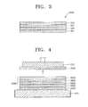
- FIG. 3 is a cross-sectional view of the filling film 500A for forming the filling material 500 of the organic light-emitting display apparatus 10 of FIG. 1 .
- the filling film 500A includes the filling material 500, a first releasing film 501 attached to a first surface of the filling material 500, a second releasing film 502 attached to a second surface of the filling material 500, and a supporting layer 503 attached on the second releasing film 502.
- the filling material 500 preferably may have a thickness in a range from about 10 ⁇ m to about 30 ⁇ m, preferably from about 20 ⁇ m to about 25 ⁇ m, and as noted above, may be formed of at least one of an epoxy resin, an acryl resin, silicon, ethylene vinyl acetate (EVA), and polyethylene.
- an epoxy resin preferably from about 10 ⁇ m to about 30 ⁇ m, preferably from about 20 ⁇ m to about 25 ⁇ m, and as noted above, may be formed of at least one of an epoxy resin, an acryl resin, silicon, ethylene vinyl acetate (EVA), and polyethylene.
- EVA ethylene vinyl acetate
- the first and second releasing films 501 and 502 protect the filling material 500 and are separated from the filling material 500 during a manufacturing process of the organic light-emitting display apparatus 10.
- the first and second releasing films 501 and 502 each may preferably independently include, for example, at least one of a polymethylpentene film, a polyethylene terephthalate (PET) film, a Teflon® film, and a polypropylene film.
- PET polyethylene terephthalate
- Teflon® film Teflon® film
- polypropylene film a polypropylene film.
- at least one of the first and second releasing films comprises PET, preferably both films comprise PET.
- the first and second releasing films 501 and 502 may be sequentially separated from the filling material 500 during a process of manufacturing the organic light-emitting display apparatus 10. More specifically, according to one embodiment, the second releasing film 502 may be separated from the filling material 500 before the first releasing film 501 is separated from the filling material 500. Accordingly, in this case, the first releasing film 501 should remain attached to the filling material 500 while the second releasing film 502 is separated. Thus, in an embodiment of the present invention a bonding force between the first releasing film 501 and the filling material 500 should preferably be greater than the bonding force between the second releasing film 502 and the filling material 500.
- the first releasing film 501 may preferably be thicker than the second releasing film 502.
- the first releasing film 501 may have a thickness in a range from about 50 ⁇ m to about 150 ⁇ m, optionally about 50 ⁇ m to about 100 ⁇ m or about 75 ⁇ m to about 125 ⁇ m.
- the second releasing film 502 may preferably have a thickness in a range from about 10 ⁇ m to about 50 ⁇ m, preferably about 20 ⁇ m to about 50 ⁇ m, more preferably about 20 ⁇ m to about 35 ⁇ m.
- the bonding force between the first releasing film 501 and the filling material 500 is greater than the bonding force between the second releasing film 502 and the filling material 500, and thus, the process of manufacturing the organic light-emitting display apparatus 10 may be stably performed.
- the supporting layer 503 is attached to the second releasing film 502, increases the overall thickness and weight of the filling film 500A, and may prevent the filling film 500A from bending or wrinkling due to a pressure applied to a lateral side of the filling film 500A.
- the supporting layer 503 may include, for example, PET, but it is not limited thereto. Accordingly, in an embodiment of the present invention, the supporting layer comprises at least one polymer selected from the group consisting of polyethylene terephthalate, polypropylene, polyethylene, polyvinyl chloride and polycarbonate, preferably polyethylene terephtalate.
- the supporting layer 503 is preferably not separated from the second releasing film 502 during the process of manufacturing the organic light-emitting display apparatus 10. Rather, preferably the supporting layer 503 is separated from the filling material 500 together with the second releasing film 502 when the second releasing film 502 is separated from the filling material 500. Accordingly, a bonding force between the supporting layer 503 and the second releasing film 502 should preferably be greater than the bonding force between the second releasing film 502 and the filling material 500.
- the supporting layer 503 may have a thickness in a range from about 50 ⁇ m to about 150 ⁇ m, optionally about 50 ⁇ m to about 100 ⁇ m or about 75 ⁇ m to about 125 ⁇ m.
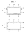
- the filling film 500A may be bent or be wrinkled by a centering pin 720 (refer to FIG. 5 ) in a process of aligning the filling film 500A, as described below with reference to FIG. 5 .
- the supporting layer 503 when the supporting layer 503 is less than 50 ⁇ m thick, a bonding force between the supporting layer 503 and the second releasing film 502 is reduced, and thus, the supporting layer 503 may be separated from the second releasing film 502 when the second releasing film 502 is separated from the filling material 500, thereby reducing the efficiency of manufacturing the organic light-emitting display apparatus 10.
- the supporting layer 503 When the supporting layer 503 is more than 150 ⁇ m (preferbaly 100 ⁇ m) thick, the weight of the filling film 500A is excessively increased, and as a result, the filling film 500A may not be lifted by a pick-up unit 620 (refer to FIG. 4 ). Accordingly, the supporting layer 503 may have a thickness in a range from about 50 ⁇ m to about 100 ⁇ m.
- An upper surface of the supporting layer 503 may preferably be static shielded.
- the static shielding may be obtained by coating an anti-static agent on the upper surface of the supporting layer 503. Other methods may be used to obtain the static-shielding. For example, the static shielding may be achieved when the supporting layer 503 includes an anti-static agent.
- the pick-up unit 620 (refer to FIG. 4 ) may easily lift the filling films 500A sheet-by-sheet.
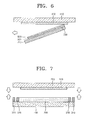
- FIGS. 4 through 7 are schematic cross-sectional views illustrating a method of manufacturing the organic light-emitting display apparatus 10 of FIG. 1 .
- the method described below relates to the manufacture of an organic light-emitting display apparatus, embodiments of the present invention may be applied to any display apparatus or light emitter that is sealed for its protection, such as protection from impact, air, or moisture.
- the method of manufacturing the organic light-emitting display apparatus 10, according to an embodiment of the present invention includes: separating the filling films 500A sheet-by-sheet from the layer stack 500B; aligning a separated filling film 500A on the center of a film stage 710; laminating the filling material 500 of the aligned filling film 500A with the encapsulation substrate 400; and combining the substrate 100 on which the display unit 200 is formed with the encapsulation substrate 400.
- the separating of the filling films 500A sheet-by-sheet from the layer stack 500B includes, as depicted in FIG. 4 , lifting the filling films 500A sheet-by-sheet from the layer stack 500B, which is formed by stacking a plurality of the filling films 500A, by the pick-up unit 620.
- the pick-up unit 620 includes a vacuum pad (not shown), and the vacuum pad lifts the uppermost filling film 500A of the layer stack 500B by a vacuum force after the vacuum pad contacts an upper surface of the layer stack 500B. In some embodiments, due to the vacuum force, the pick-up unit 620 may lift the uppermost filling film 500A without actually contacting the uppermost filling film 500A,
- Stacked filling films may generate static electricity due to friction.
- An electrostatic force may act between the two filling films that contact each other, and thus, the filling films may not be easily separated sheet-by-sheet.
- an error may occur in the process of manufacturing the organic light-emitting display apparatus 10, thereby reducing manufacturing efficiency.
- the filling film 500A further includes the supporting layer 503 besides the filling material 500 and the first and second releasing films 501 and 502 attached to both surfaces of the filling material 500, an overall weight of the filling film 500A may be increased. Accordingly, the filling films 500A may be readily lifted sheet-by-sheet by the pick-up unit 620. Also, the pick-up unit 620 may perform a shaking operation at least once while lifting the filling films 500A. Due to the detaching operation of the pick-up unit 620, even if two or more sheets of the filling films 500A are lifted, the filling films 500A may be readily separated sheet-by-sheet due to the increased weight by the supporting layer 503.
- the upper surface of the supporting layer 503 may be static shielded.
- the generation of static electricity between the stacked filling films 500A may be prevented or reduced.
- the separation operation of the filling films 500A may be effectively performed.
- the filling films 500A may be more easily picked up on a sheet-by-sheet basis, and in the case that two or more filling films 500A are picked up, they may be more readily separated due to the shaking operation of the pick-up unit 620, thereby leaving a single filling film 500A attached to the pick-up unit 620.
- the filling film 500A includes the filing material 500, the first releasing film 501, and the second releasing film 502, but does not include the supporting layer 503.
- the filling film 500A additionally includes the supporting layer 503.
- the upper surface of the supporting layer 503 is static shielded.
- the filling film 500A includes the filling material 500 having a thickness of 20 ⁇ m, the first releasing film 501 having a thickness of 100 ⁇ m, and the second releasing film 502 having a thickness of 25 ⁇ m.
- the supporting layer 503 has a thickness of 100 ⁇ m.
- the supporting layer when present, is formed of PET
- the filling material is formed of epoxy resin
- the first and second releasing films are formed of PET.
- a separated filling film 500A is aligned on the film stage 710.
- the filling film 500A is aligned by centering pins 720 that move from an edge unit of the film stage 710 to contact side surfaces of the filling film 500A.
- the aligned filling film 500A may be adsorbed by and fixed on vacuum holes formed on a surface of the film stage 710.
- the centering pins 720 apply forces on the four sides of the filling film 500A. At this point, if the filling film 500A has a very small thickness, the filling film 500A may bend or be wrinkled due to the pressure applied by the centering pins 720. In this case, the filling film 500A may not be aligned well and may cause an error in a subsequent process.
- the filling film 500A further includes the supporting layer 503 besides the filling material 500 and the first and second releasing films 501 and 502 that are attached to both sides of the filling material 500, the thickness of the filling film 500A is increased. Therefore, the bending or wrinkling of the filling film 500A due to the pressure applied to side surfaces of the filling film 500A by the centering pins 720 may be prevented.
- Table 2 summarizes success rates of the centering operations.
- “success” means that the filling film 500A was not bent or wrinkled enough to cause an error in a subsequent process.
- the filling film 500A does not include the supporting layer 503.
- the filling film 500A includes the supporting layer 503.
- the filling films 500A used in the comparative example and embodiment were the same filling films 500A used in the separation operations of Table 1.
- the filling material 500 of the filling film 500A may be disposed on the encapsulation substrate 400.
- the filling material 500 may be laminated with the encapsulation substrate 400.
- the encapsulation substrate 400 is fixed on a substrate stage 410, and the encapsulation substrate 400 may be disposed to face the ground.
- the substrate stage 410 may be fixed with the encapsulation substrate 400 by adsorbing the encapsulation substrate 400 by a vacuum.
- the supporting layer 503 and the second releasing film 502 are separated from the filling material 500, and the exposed filling material 500 is disposed to face the encapsulation substrate 400. Also, the first releasing film 501 is maintained in a combined state with the filling material 500. For this purpose, a bonding force between the supporting layer 503 and the second releasing film 502 is greater than the bonding force between the second releasing film 502 and the filling material 500, and a bonding force between the first releasing film 501 and the filling material 500 is greater than the bonding force between the second releasing film 502 and the filling material 500.
- the lamination of the encapsulation substrate 400 with the filling material 500 may preferably be performed by rotatably moving a roller 730 included on a side of the film stage 710 in a direction. That is, the lamination may be performed in a direction indicated by an arrow in FIG. 6 from a point that contacts the encapsulation substrate 400 as a starting point at a side of the filling material 500.
- the first releasing film 501 may be removed after the filling material 500 is laminated on a surface of the encapsulation substrate 400.
- the encapsulation substrate 400 and the substrate 100 on which the display unit 200 is formed are combined by using the sealing material 310 as a medium.
- the display unit 200 is described with reference to FIG. 2 .
- various organic light-emitting displays that are well known in the art may be applied to the current embodiment, and thus, descriptions of practical methods of manufacturing the organic light-emitting displays are omitted.
- the sealing material 310 may be formed to surround the filling material 500 on the encapsulation substrate 400.
- the sealing material 310 may be formed by coating a liquid or paste sealing material.
- FIG. 7 it is depicted that the sealing material 310 is formed on a surface of the encapsulation substrate 400, but other configurations are possible.
- the sealing material 310 may be formed on a surface of the substrate 100.
- the moisture absorbent 320 may further be formed on an inner side of the sealing material 310.
- the moisture absorbent 320 may be formed by coating a liquid moisture absorbent 320.
- the combination of the substrate 100 and the encapsulation substrate 400 is performed such that, after separating the first releasing film 501 from the filling material 500, the substrate 100 is disposed to face the encapsulation substrate 400, and afterwards, the substrate 100 and the encapsulation substrate 400 are combined by irradiating ultraviolet (UV) rays onto the substrate 100 that corresponds to the sealing material 310 and the encapsulation substrate 400 in a vacuum state.
- UV ultraviolet
- the substrate 100 and the encapsulation substrate 400 when UV rays are irradiated onto the substrate 100 and the encapsulation substrate 400, portions of the substrate 100 and the encapsulation substrate 400 that contact the sealing material 310 melt, and thus, the substrate 100 and the encapsulation substrate 400 may be adhered.
Landscapes
- Engineering & Computer Science (AREA)
- Manufacturing & Machinery (AREA)
- Physics & Mathematics (AREA)
- Microelectronics & Electronic Packaging (AREA)
- General Physics & Mathematics (AREA)
- Theoretical Computer Science (AREA)
- Computer Hardware Design (AREA)
- Optics & Photonics (AREA)
- Electroluminescent Light Sources (AREA)
Abstract
Description
- Embodiments of the present invention relate to a filling film and a method of manufacturing an organic light-emitting display apparatus by using the same, and more particularly, to a filling film that can increase a manufacturing efficiency of an organic light-emitting display apparatus and a method of manufacturing the organic light-emitting display apparatus by using the same.
- Recently, display apparatuses have been replaced by portable thin film flat display apparatuses. Of the flat display apparatuses, a field emission display apparatus is an emissive display apparatus that has wide viewing angles and high contrast, and thus, draws attention as a next generation display apparatus. Also, an organic light-emitting display apparatus, in which a light-emitting layer is formed of an organic material, has desirable characteristics, such as wide viewing angles, high contrast, short response times, and multi-color displays.
- An organic light-emitting display apparatus typically includes a substrate on which a display unit is formed and an encapsulating substrate formed on the display unit, and the substrate and the encapsulating substrate are combined with each other by using a sealant. However, due to the trend of increasing the size of the organic light-emitting display apparatus, the size and weight of the encapsulating substrate are also increased. Thus, in order to ensure the structural reliability of the organic light-emitting display apparatus, a method of further including a filling material between the substrate and the encapsulating substrate has been developed.
- Embodiments of the present invention provide a filling film as claimed in claims 1 to 9 that can increase a manufacturing efficiency of an organic light-emitting display apparatus and a method of manufacturing the organic light-emitting display apparatus by using the filling film as claimed in
claims 10 to 16. - An embodiment of the present invention discloses a filling films. The filling film comprises a filling material, a first releasing film attached to a first surface of the filling material, a second releasing film attached to a second surface of the filling material, and a supporting layer attached to the second releasing film. A bonding force between the second releasing film and the supporting layer is preferably greater than a bonding force between filling material and the second releasing film.
- An embodiment of the present invention also discloses a method of manufacturing a display apparatus. The method includes separating a filling film from a stack in which a plurality of the filling films are stacked, centering the separated filling film on a film stage, laminating a filling material of the filling film on an encapsulation substrate, and combining the encapsulation substrate and a substrate comprising a display unit. Prior to laminating, the filling film preferably comprises a first releasing film attached to a first surface of the filling material, a second releasing film attached to a second surface of the filling material, and a supporting layer attached to the second releasing film, and the supporting layer comprises polyethylene terephthalate and has a thickness in a range from about 50 µm to about 100 µm.
- An embodiment of the present invention also discloses a first releasing film having a first thickness, a filling material disposed on the first releasing film, a second releasing film disposed on the filling materials and having a second thickness, the second thickness being less than the first thickness, and a supporting layer disposed on the second releasing film. The supporting layer includes polyethylene terephtalate and has a third thickness greater than the second thickness.
- It is to be understood that both the foregoing general description and the following detailed description are explanatory and are intended to provide further explanation of the invention as claimed.
- The above and other features and advantages of the present invention will become more apparent by describing in detail embodiments thereof with reference to the attached drawings.
-
FIG. 1 is a schematic cross-sectional view of an organic light-emitting display apparatus according to an embodiment of the present invention. -
FIG. 2 is a schematic cross-section al view of a display unit of the organic light-emitting display apparatus ofFIG. 1 . -
FIG. 3 is a cross-sectional view of a filling film for forming a filling material of the organic light-emitting display apparatus ofFIG. 1 . -
FIG. 4 ,FIG. 5A ,FIG. 5B ,FIG. 6, and FIG. 7 are schematic cross-sectional views illustrating a method of manufacturing the organic light-emitting display apparatus ofFIG. 1 . - While embodiments are capable of various modifications and alternative forms, embodiments thereof are shown by way of example in the drawings and will herein be described in detail. It should be understood, however, that there is no intent to limit embodiments to the particular forms disclosed, but on the contrary, embodiments are to cover all modifications, equivalents, and alternatives falling within the scope of the invention. In describing the present invention, when practical descriptions with respect to related known function and configuration may unnecessarily make unclear of the scope of the present invention, the descriptions thereof will be omitted.
- It will be understood that, although the terms "first", "second", etc. may be used herein to describe various elements, these elements should not be limited by these terms. These terms are only used to distinguish one element from another.
- It will be understood that when an element or layer is referred to as being "on" or "connected to" another element or layer, it can be directly on or directly connected to the other element or layer, or intervening elements or layers may be present. In contrast, when an element is referred to as being "directly on" or "directly connected to" another element or layer, there are no intervening elements or layers present. It will be understood that for the purposes of this disclosure, "at least one of X, Y, and Z" can be construed as X only, Y only, Z only, or any combination of two or more items X, Y, and Z (e.g., XYZ, XYY, YZ, ZZ).
- Hereafter, the present invention will be described more fully with reference to the accompanying drawings, in which embodiments of the present invention are shown. In describing embodiments of the present invention with reference to drawings, like reference numerals are used for elements that are substantially identical or correspond to each other, and the descriptions thereof will not be repeated. In the drawings, thicknesses may be magnified for clarity of layers and regions. Also, for convenience of explanation, some of the layers and regions may be exaggerated.
-
FIG. 1 is a schematic cross-sectional view of an organic light-emittingdisplay apparatus 10 according to an embodiment of the present invention.FIG. 2 is a schematic cross-sectional view of adisplay unit 200 of the organic light-emittingdisplay apparatus 10 ofFIG. 1 . - Referring to
FIGS. 1 and 2 , the organic light-emitting display apparatus 10 includes asubstrate 100, thedisplay unit 200 formed on thesubstrate 100, anencapsulation substrate 400 disposed to face thesubstrate 100, asealing material 310 that seals thedisplay unit 200 by combining thesubstrate 100 and theencapsulation substrate 400, and afilling material 500 between thedisplay unit 200 and theencapsulation substrate 400. - The
substrate 100 may be formed of a transparent glass material having SiO2 as the main component. However, thesubstrate 100 may be formed using other materials. For example, the substrate may be formed of a transparent plastic material. The plastic material used to form thesubstrate 100 may include, for example, at least one insulating organic material such as polyethersulphone (PES), polyacrylate (PAR), polyetherimide (PEI), polyethylene naphthalate (PEN), polyethylene terephthalate (PET), polyphenylene sulfide (PPS), polyallylate, polyimide, polycarbonate (PC), triacetate (TAC), and cellulose acetate propionate (CAP). - When the organic light-
emitting display apparatus 10 is a bottom emission type, in which an image is realized in a direction towards thesubstrate 100, thesubstrate 100 is formed of a transparent material. However, when the organic light-emitting display apparatus 10 is a top emission type, in which an image is realized in a direction opposite to thesubstrate 100, thesubstrate 100 may be formed of a reflective material, such as a metallic material. When thesubstrate 100 is formed of a metallic material, thesubstrate 100 may include, for example, at least one of carbon, iron, chrome, manganese, nickel, titanium, molybdenum, and stainless steel (SUS). - The
display unit 200 may include a thinfilm transistor layer 200a and apixel unit 200b. The thinfilm transistor layer 200a may be formed using organic, inorganic, or any other materials that may be used to form thin film transistors. Thepixel unit 200b may be an organic light-emitting device (OLED). Hereinafter, thedisplay unit 200 will be described in detail with reference toFIG. 2 . - A
buffer layer 212 may be formed on thesubstrate 100. Thebuffer layer 212 prevents the penetration of impurity elements into thesubstrate 100 and provides a planarized surface on thesubstrate 100. Thebuffer layer 212 may be formed of various materials that perform the functions described above. For example, thebuffer layer 212 may include, for example, at least one inorganic material such as silicon oxide, silicon nitride, silicon oxynitride, aluminum oxide, aluminum nitride, titanium oxide, and titanium nitride or at least one organic material such as polyimide, polyester, and acryl, and may be formed as a stack of layers by using the materials described above. - The
buffer layer 212 may be deposited by using various methods, for example, a plasma-enhanced chemical vapor deposition (PECVD) method, an atmospheric pressure CVD (APCVD) method, or a low pressure CVD (LPCVD). - An
active layer 221 may be formed of an inorganic semiconductor, such as silicon, or an organic semiconductor on thebuffer layer 212. Also, theactive layer 221 includes a source region, a drain region, and a channel region between the source and drain regions. For example, when theactive layer 221 is formed of amorphous silicon, theactive layer 221 may be formed such that, after forming an amorphous silicon layer on the whole surface of thebuffer layer 212, a polycrystalline silicon layer is formed by crystallizing the amorphous silicon layer. After patterning the polycrystalline silicon layer, theactive layer 221 having the source region and the drain region on edges thereof and the channel region between the source region and the drain region is formed by doping the source drain regions with a dopant. - A
gate insulating film 213 is formed on theactive layer 221. Thegate insulating film 213 is formed to insulate theactive layer 221 from agate electrode 222, and may be formed of an inorganic material, such as SiNx or SiO2. - The
gate electrode 222 is formed in on an upper surface of thegate insulating film 213. Thegate electrode 222 is connected to a gate line (not shown) via which an On/Off signal is applied to a thin film transistor (TFT). - The
gate electrode 222 may include, for example, at least one metallic material such as Au, Ag, Cu, Ni, Pt, Pd, Al, and Mo, and may include an alloy, such as Al:Nd or Mo: W. However, thegate electrode 222 may be formed of other materials in consideration of design conditions. - An interlayer insulating
layer 214 formed on thegate electrode 222 is formed to insulate between thegate electrode 222 and source and drainelectrodes 223 and may be formed of an inorganic material, such as SiNx or SiO2. - The source and drain
electrodes 223 are formed on theinterlayer insulating layer 214. More specifically, contact holes are formed in theinterlayer insulating layer 214 and thegate insulating film 213 to expose the source region and the drain region of theactive layer 221, and the source and drainelectrodes 223 are electrically connected to the exposed source region and the drain region of theactive layer 221 through the contact holes. -
FIG. 2 depicts a top gate type TFT, which sequentially includes theactive layer 221, thegate electrode 222, and the source and drainelectrodes 223. However, the TFT may have other structures. For example, thegate electrode 222 may be disposed under theactive layer 221. - The organic thin
film transistor layer 200a described above is electrically connected to thepixel unit 200b to drive thepixel unit 200b, and is protected by being covered by aplanarizing film 215. - The
planarizing film 215 may be an inorganic insulating film and/or an organic insulating films. The inorganic insulating film may include, for example, at least one of SiO2, SiNx, SiON, Al2O3, TiO2, Ta2O5, HfO2, ZrO2, BST, and PZT. The organic insulating film may include, for example, at least one of a general purpose polymer, such as polymethylmethacrylate (PMMA) or polystyrene (PS), a polymer derivative having a phenol group, an acryl polymer, an imide polymer, an aryl ether polymer, an amide polymer, a fluoride polymer, a p-gilyrene polymer, a vinyl alcohol polymer, and a blend of these materials. Also, theplanarizing film 215 may be formed as a complex stacking layer of an inorganic insulating film and an organic insulating film. - The
pixel unit 200b is formed on theplanarizing film 215. Thepixel unit 200b may include apixel electrode 231, anintermediate layer 232, and a facingelectrode 233. - The
pixel electrode 231 is formed on theplanarizing film 215 and is electrically connected to ether the source ordrain electrode 223 through acontact hole 230 formed in theplanarizing film 215. - The
pixel electrode 231 may be a reflection electrode, and in this case, it may include a reflection film including, for example, at least one of Ag, Mg, Al, Pt, Pd, Au, Ni, Nd, Ir, Cr, and a compound of these materials, as well as a transparent or semitransparent electrode formed on the reflection film. The transparent or semitransparent electrode may include, for example, at least one of indium tin oxide (ITO), indium zinc oxide (IZO), zinc oxide (ZnO), indium oxide (In2O3), indium gallium oxide (IGO), and aluminum zinc oxide (AZO). - The facing
electrode 233 facing thepixel electrode 231 may be a transparent or semitransparent electrode, and may be formed of a metal thin film having a small work function. The metal thin film may include, for example, at least one of Li, Ca, LiF/Ca, LiF/Al, Al, Ag, Mg, and a compound of these materials. Also, an auxiliary electrode layer or a bus electrode that is formed of a material used to form a transparent electrode, for example, ITO, IZO, ZnO, or In2O3, may further be formed on the metal thin film, - Accordingly, the facing
electrode 233 may transmit light emitted from an organic light-emitting layer (not shown) included in theintermediate layer 232. That is, light emitted from the organic light-emitting layer may be directly discharged towards the facingelectrode 233 or by being reflected by thepixel electrode 231 that is formed as a reflection electrode. - The organic light-emitting
display apparatus 10 may have other configurations. For example, the organic light-emittingdisplay apparatus 10 may be a bottom emission type organic light-emitting display apparatus in which light is discharged towards thesubstrate 100. When the organic light-emittingdisplay apparatus 10 is a bottom emission type, thepixel electrode 231 may be formed as a transparent or semitransparent electrode, and the facingelectrode 233 may be formed as a reflection electrode. Also, the organic light-emittingdisplay apparatus 10 may be a dual light-emitting display apparatus in which light is emitted in both top and bottom directions. - A pixel-defining
film 216 is formed on thepixel electrode 231 using an insulating material. The pixel-definingfilm 216 may include, for example, at least one of polyimide, polyamide, acryl resin, benzocyclobutene, and phenol resin by using a spin coating method. The pixel-definingfilm 216 exposes a portion of thepixel electrode 231, and theintermediate layer 232, which includes the organic light-emitting layer, is located on the exposed portion of thepixel electrode 231, - The organic light-emitting layer (not shown) included in the
intermediate layer 232 may be formed of a low molecular weight organic material or a polymer organic material. Theintermediate layer 232 may further optionally include functional layers, such as a hole transport layer (HTL), a hole injection layer (HIL), an electron transport layer (ETL), and an electron injection layer (EIL), besides the organic light-emitting layer. - The
substrate 100, on which thedisplay unit 200 is included, is combined with theencapsulation substrate 400 that is disposed on thedisplay unit 200. Theencapsulation substrate 400 may be formed of various materials. For example, theencapsulation substrate 400 may be formed of plastic materials, such as acryl, besides a glass material, and furthermore, may be formed of a metal plate. - The
substrate 100 and theencapsulation substrate 400 are combined by using the sealingmaterial 310. The sealingmaterial 310 may be a generally-used material, such as sealing glass frit. The sealingmaterial 310 and theencapsulation substrate 400 block external moisture or air from reaching thedisplay unit 200. - A
moisture absorbent 320 may further be disposed on a side of the sealingmaterial 310. Themoisture absorbent 320 readily reacts with moisture and oxygen, and thus, prevents reduction of the OLED's lifetime due to the moisture and oxygen. Themoisture absorbent 320 may include, for example, at least one of an alkali metal oxide, an alkali-earth metal oxide, a metal halide, lithium sulfate, metal sulphate, metal perchlorate, and one of silica gel and phosphorous pentoxide, or a mixture of these materials. However, the type and location of themoisture absorbent 320 can have various other configurations. - The filling
material 500 is included inside the area that is sealed by the sealingmaterial 310. The fillingmaterial 500 is included to fill a space between thesubstrate 100 and theencapsulation substrate 400. - The filling
material 500 may include, for example, at least one of an epoxy resin, an acryl resin, silicon, ethylene vinyl acetate (EVA), and polyethylene. In a preferred embodiment of the present invention, the filling material comprises an epoxy resin. The fillingmaterial 500 may have a thickness T in a range from about 10 µm to about 30 µm. The fillingmaterial 500 may have a thermo-hardening or ultraviolet (UV) ray hardening characteristic, and may include various additives, such as a hardening agent, an antioxidant, and a coupling agent. - The filling
material 500 described above may be formed by using afilling film 500A depicted inFIG. 3 . The fillingfilm 500A will now be described in detail with reference toFIG. 3 . -
FIG. 3 is a cross-sectional view of the fillingfilm 500A for forming the fillingmaterial 500 of the organic light-emittingdisplay apparatus 10 ofFIG. 1 . - Referring to
FIG. 3 , the fillingfilm 500A includes the fillingmaterial 500, a first releasing film 501 attached to a first surface of the fillingmaterial 500, a second releasing film 502 attached to a second surface of the fillingmaterial 500, and a supportinglayer 503 attached on the second releasing film 502. - The filling
material 500 preferably may have a thickness in a range from about 10 µm to about 30 µm, preferably from about 20 µm to about 25 µm, and as noted above, may be formed of at least one of an epoxy resin, an acryl resin, silicon, ethylene vinyl acetate (EVA), and polyethylene. - The first and second releasing films 501 and 502 protect the filling
material 500 and are separated from the fillingmaterial 500 during a manufacturing process of the organic light-emittingdisplay apparatus 10. The first and second releasing films 501 and 502 each may preferably independently include, for example, at least one of a polymethylpentene film, a polyethylene terephthalate (PET) film, a Teflon® film, and a polypropylene film. In a preferred embodiment of the present invention, at least one of the first and second releasing films comprises PET, preferably both films comprise PET. - As described below, the first and second releasing films 501 and 502 may be sequentially separated from the filling
material 500 during a process of manufacturing the organic light-emittingdisplay apparatus 10. More specifically, according to one embodiment, the second releasing film 502 may be separated from the fillingmaterial 500 before the first releasing film 501 is separated from the fillingmaterial 500. Accordingly, in this case, the first releasing film 501 should remain attached to the fillingmaterial 500 while the second releasing film 502 is separated. Thus, in an embodiment of the present invention a bonding force between the first releasing film 501 and the fillingmaterial 500 should preferably be greater than the bonding force between the second releasing film 502 and the fillingmaterial 500. - For this purpose, in this embodiment, the first releasing film 501 may preferably be thicker than the second releasing film 502. For example, the first releasing film 501 may have a thickness in a range from about 50 µm to about 150 µm, optionally about 50 µm to about 100 µm or about 75 µm to about 125 µm. In an embodiment of the present invention, the second releasing film 502 may preferably have a thickness in a range from about 10 µm to about 50 µm, preferably about 20 µm to about 50 µm, more preferably about 20 µm to about 35 µm. Hence, because the first releasing film 501 is thicker than the second releasing film 502, the bonding force between the first releasing film 501 and the filling
material 500 is greater than the bonding force between the second releasing film 502 and the fillingmaterial 500, and thus, the process of manufacturing the organic light-emittingdisplay apparatus 10 may be stably performed. - The supporting
layer 503 is attached to the second releasing film 502, increases the overall thickness and weight of the fillingfilm 500A, and may prevent thefilling film 500A from bending or wrinkling due to a pressure applied to a lateral side of the fillingfilm 500A. - The supporting
layer 503 may include, for example, PET, but it is not limited thereto. Accordingly, in an embodiment of the present invention, the supporting layer comprises at least one polymer selected from the group consisting of polyethylene terephthalate, polypropylene, polyethylene, polyvinyl chloride and polycarbonate, preferably polyethylene terephtalate. - The supporting
layer 503 is preferably not separated from the second releasing film 502 during the process of manufacturing the organic light-emittingdisplay apparatus 10. Rather, preferably the supportinglayer 503 is separated from the fillingmaterial 500 together with the second releasing film 502 when the second releasing film 502 is separated from the fillingmaterial 500. Accordingly, a bonding force between the supportinglayer 503 and the second releasing film 502 should preferably be greater than the bonding force between the second releasing film 502 and the fillingmaterial 500. - To achieve this greater bonding force, the supporting
layer 503 may have a thickness in a range from about 50 µm to about 150 µm, optionally about 50 µm to about 100 µm or about 75 µm to about 125 µm.. When the supportinglayer 503 is less than 50 µm thick, the fillingfilm 500A may be bent or be wrinkled by a centering pin 720 (refer toFIG. 5 ) in a process of aligning the fillingfilm 500A, as described below with reference toFIG. 5 . Also, when the supportinglayer 503 is less than 50 µm thick, a bonding force between the supportinglayer 503 and the second releasing film 502 is reduced, and thus, the supportinglayer 503 may be separated from the second releasing film 502 when the second releasing film 502 is separated from the fillingmaterial 500, thereby reducing the efficiency of manufacturing the organic light-emittingdisplay apparatus 10. - When the supporting
layer 503 is more than 150 µm (preferbaly 100 µm) thick, the weight of the fillingfilm 500A is excessively increased, and as a result, the fillingfilm 500A may not be lifted by a pick-up unit 620 (refer toFIG. 4 ). Accordingly, the supportinglayer 503 may have a thickness in a range from about 50 µm to about 100 µm. - An upper surface of the supporting
layer 503 may preferably be static shielded. The static shielding may be obtained by coating an anti-static agent on the upper surface of the supportinglayer 503. Other methods may be used to obtain the static-shielding. For example, the static shielding may be achieved when the supportinglayer 503 includes an anti-static agent. - In this way, when the upper surface of the supporting
layer 503 is static shielded, as depicted inFIG. 4 , when alayer stack 500B is formed by stacking a plurality of fillingfilms 500A, the action of electrostatic force between the fillingfilms 500A may be prevented. Thus, the pick-up unit 620 (refer toFIG. 4 ) may easily lift the fillingfilms 500A sheet-by-sheet. -
FIGS. 4 through 7 are schematic cross-sectional views illustrating a method of manufacturing the organic light-emittingdisplay apparatus 10 ofFIG. 1 . Although the method described below relates to the manufacture of an organic light-emitting display apparatus, embodiments of the present invention may be applied to any display apparatus or light emitter that is sealed for its protection, such as protection from impact, air, or moisture. - The method of manufacturing the organic light-emitting
display apparatus 10, according to an embodiment of the present invention, includes: separating the fillingfilms 500A sheet-by-sheet from thelayer stack 500B; aligning a separated fillingfilm 500A on the center of afilm stage 710; laminating the fillingmaterial 500 of the aligned fillingfilm 500A with theencapsulation substrate 400; and combining thesubstrate 100 on which thedisplay unit 200 is formed with theencapsulation substrate 400. - Hereinafter, the method of manufacturing the organic light-emitting
display apparatus 10 will now be described in detail with reference toFIG. 3 andFIGS. 4 through 7 . - The separating of the filling
films 500A sheet-by-sheet from thelayer stack 500B includes, as depicted inFIG. 4 , lifting the fillingfilms 500A sheet-by-sheet from thelayer stack 500B, which is formed by stacking a plurality of the fillingfilms 500A, by the pick-upunit 620. - The pick-up
unit 620 includes a vacuum pad (not shown), and the vacuum pad lifts theuppermost filling film 500A of thelayer stack 500B by a vacuum force after the vacuum pad contacts an upper surface of thelayer stack 500B. In some embodiments, due to the vacuum force, the pick-upunit 620 may lift theuppermost filling film 500A without actually contacting theuppermost filling film 500A, - Stacked filling films may generate static electricity due to friction. An electrostatic force may act between the two filling films that contact each other, and thus, the filling films may not be easily separated sheet-by-sheet. When two sheets of the filling films are simultaneously lifted and enter to a centering process like that depicted in
FIG. 5 , an error may occur in the process of manufacturing the organic light-emittingdisplay apparatus 10, thereby reducing manufacturing efficiency. - However, according to embodiments of the present invention, since the filling
film 500A further includes the supportinglayer 503 besides the fillingmaterial 500 and the first and second releasing films 501 and 502 attached to both surfaces of the fillingmaterial 500, an overall weight of the fillingfilm 500A may be increased. Accordingly, the fillingfilms 500A may be readily lifted sheet-by-sheet by the pick-upunit 620. Also, the pick-upunit 620 may perform a shaking operation at least once while lifting the fillingfilms 500A. Due to the detaching operation of the pick-upunit 620, even if two or more sheets of the fillingfilms 500A are lifted, the fillingfilms 500A may be readily separated sheet-by-sheet due to the increased weight by the supportinglayer 503. - Also, according to embodiments of the present invention, the upper surface of the supporting
layer 503 may be static shielded. Thus, the generation of static electricity between thestacked filling films 500A may be prevented or reduced. Accordingly, the separation operation of the fillingfilms 500A may be effectively performed. In other words, the fillingfilms 500A may be more easily picked up on a sheet-by-sheet basis, and in the case that two or more fillingfilms 500A are picked up, they may be more readily separated due to the shaking operation of the pick-upunit 620, thereby leaving asingle filling film 500A attached to the pick-upunit 620. - Table 1 summarizes success rates of the separation operations. Here, "success" means that a
single filling film 500A was initially picked up by the pick-upunit 620, or in the case that two or more fillingfilms 500A were picked up, the shaking operation of the pick-upunit 620 resulted in leaving asingle filling film 500A attached to the pick-upunit 620. In the comparative example, the fillingfilm 500A includes thefiling material 500, the first releasing film 501, and the second releasing film 502, but does not include the supportinglayer 503. However, in embodiments 1 and 2, the fillingfilm 500A additionally includes the supportinglayer 503. Also, unlike embodiment 1, in embodiment 2, the upper surface of the supportinglayer 503 is static shielded. The fillingfilm 500A includes the fillingmaterial 500 having a thickness of 20 µm, the first releasing film 501 having a thickness of 100 µm, and the second releasing film 502 having a thickness of 25 µm. The supportinglayer 503 has a thickness of 100 µm. In the comparative example and embodiments, i) the supporting layer, when present, is formed of PET, ii) the filling material is formed of epoxy resin, and ii) the first and second releasing films are formed of PET.[Table 1] Success rate Comparative example 50% Embodiment 1 95% Embodiment 2 100% - Next, as depicted in
FIG. 5 , a separated fillingfilm 500A is aligned on thefilm stage 710. - More specifically, when a filling
film 500A is placed on thefilm stage 710, the fillingfilm 500A is aligned by centeringpins 720 that move from an edge unit of thefilm stage 710 to contact side surfaces of the fillingfilm 500A. The alignedfilling film 500A may be adsorbed by and fixed on vacuum holes formed on a surface of thefilm stage 710. - The centering pins 720 apply forces on the four sides of the filling
film 500A. At this point, if the fillingfilm 500A has a very small thickness, the fillingfilm 500A may bend or be wrinkled due to the pressure applied by the centering pins 720. In this case, the fillingfilm 500A may not be aligned well and may cause an error in a subsequent process. - However, according to embodiments of the present invention, since the filling
film 500A further includes the supportinglayer 503 besides the fillingmaterial 500 and the first and second releasing films 501 and 502 that are attached to both sides of the fillingmaterial 500, the thickness of the fillingfilm 500A is increased. Therefore, the bending or wrinkling of the fillingfilm 500A due to the pressure applied to side surfaces of the fillingfilm 500A by the centeringpins 720 may be prevented. - Table 2 summarizes success rates of the centering operations. Here, "success" means that the filling
film 500A was not bent or wrinkled enough to cause an error in a subsequent process. In the comparative example, like the comparative example above, the fillingfilm 500A does not include the supportinglayer 503. However, in the embodiment, the fillingfilm 500A includes the supportinglayer 503. Also, the fillingfilms 500A used in the comparative example and embodiment were thesame filling films 500A used in the separation operations of Table 1.[Table 2] Success rate Comparative example 70% Embodiment 90% or more - As it is seen from Tables I and 2, in the case of the filling
film 500A that includes the supportinglayer 503, success rates of more than 90% are achieved, that is, the occurrence of errors may be reduced at the separation operation and the centering operation in a process of manufacturing the organic light-emittingdisplay apparatus 10. Thus, the manufacturing efficiency of the organic light-emittingdisplay apparatus 10 may be increased. - Next, as depicted in
FIG. 6 , the fillingmaterial 500 of the fillingfilm 500A may be disposed on theencapsulation substrate 400. For example, the fillingmaterial 500 may be laminated with theencapsulation substrate 400. - The
encapsulation substrate 400 is fixed on asubstrate stage 410, and theencapsulation substrate 400 may be disposed to face the ground. Thesubstrate stage 410 may be fixed with theencapsulation substrate 400 by adsorbing theencapsulation substrate 400 by a vacuum. - In the filling
film 500A aligned on thefilm stage 710, the supportinglayer 503 and the second releasing film 502 are separated from the fillingmaterial 500, and the exposed fillingmaterial 500 is disposed to face theencapsulation substrate 400. Also, the first releasing film 501 is maintained in a combined state with the fillingmaterial 500. For this purpose, a bonding force between the supportinglayer 503 and the second releasing film 502 is greater than the bonding force between the second releasing film 502 and the fillingmaterial 500, and a bonding force between the first releasing film 501 and the fillingmaterial 500 is greater than the bonding force between the second releasing film 502 and the fillingmaterial 500. - The lamination of the
encapsulation substrate 400 with the fillingmaterial 500 may preferably be performed by rotatably moving aroller 730 included on a side of thefilm stage 710 in a direction. That is, the lamination may be performed in a direction indicated by an arrow inFIG. 6 from a point that contacts theencapsulation substrate 400 as a starting point at a side of the fillingmaterial 500. - The first releasing film 501 may be removed after the filling
material 500 is laminated on a surface of theencapsulation substrate 400. - Finally, as depicted in
FIG. 7 , theencapsulation substrate 400 and thesubstrate 100 on which thedisplay unit 200 is formed are combined by using the sealingmaterial 310 as a medium. - The
display unit 200 is described with reference toFIG. 2 . However, various organic light-emitting displays that are well known in the art may be applied to the current embodiment, and thus, descriptions of practical methods of manufacturing the organic light-emitting displays are omitted. - The sealing
material 310 may be formed to surround the fillingmaterial 500 on theencapsulation substrate 400. The sealingmaterial 310 may be formed by coating a liquid or paste sealing material. InFIG. 7 , it is depicted that the sealingmaterial 310 is formed on a surface of theencapsulation substrate 400, but other configurations are possible. For example, the sealingmaterial 310 may be formed on a surface of thesubstrate 100. Also, themoisture absorbent 320 may further be formed on an inner side of the sealingmaterial 310. For example, themoisture absorbent 320 may be formed by coating aliquid moisture absorbent 320. - The combination of the
substrate 100 and theencapsulation substrate 400 is performed such that, after separating the first releasing film 501 from the fillingmaterial 500, thesubstrate 100 is disposed to face theencapsulation substrate 400, and afterwards, thesubstrate 100 and theencapsulation substrate 400 are combined by irradiating ultraviolet (UV) rays onto thesubstrate 100 that corresponds to the sealingmaterial 310 and theencapsulation substrate 400 in a vacuum state. When the combination operation is performed in a vacuum state, the penetration of external moisture and foreign materials may be reduced. - Also, when UV rays are irradiated onto the
substrate 100 and theencapsulation substrate 400, portions of thesubstrate 100 and theencapsulation substrate 400 that contact the sealingmaterial 310 melt, and thus, thesubstrate 100 and theencapsulation substrate 400 may be adhered. However, this is merely an embodiment, and thesubstrate 100 and theencapsulation substrate 400 may be adhered in various ways according to the kinds of the sealingmaterials 310. - While the present invention has been particularly shown and described with reference to embodiments thereof, it will be understood by those of ordinary skill in the art that various changes in form and details may be made therein without departing from the scope of the present invention as defined by the following claims.
Claims (16)
- A filling film, comprising:a filling material;a first releasing film attached to a first surface of the filling material;a second releasing film attached to a second surface of the filling material; anda supporting layer attached to the second releasing film.
- The filling film of claim 1, wherein the supporting layer comprises at least one polymer selected from the group consisting of polyethylene terephthalate, polypropylene, polyethylene, polyvinyl chloride and polycarbonate.
- The filling film of claim 1 or claim 2, wherein the supporting layer or the first releasing film independently each has a thickness in a range from about 50 µm to about 150 µm, optionally about 50 µm to about 100 µm or about 75 µm to about 125 µm.
- The filling film of any of claims 1 to 3, wherein a thickness of the first releasing film is greater than a thickness of the second releasing film.
- The filling film of any of claims 1 to 4, wherein a thickness of the supporting layer is greater than a thickness of the second releasing film.
- The filling film of any of claims 1 to 5, wherein the first releasing film and second releasing film each independently comprises at least one of a polymethylpentene film, a polyethylene terephthalate film, a Teflon® film, and a polypropylene film, and the second releasing film comprises at least one of a polymethylpentene film, a polyethylene terephtalate film, a Teflon® film, and a polypropylene film.
- The filling film of any of claims 1 to 6, wherein a bonding force between the second releasing film and the supporting layer is greater than a bonding force between the filling material and the second releasing film.
- The filling film of any of claims 1 to 7, wherein a bonding force between the first releasing film and the filling material is greater than a bonding force between the second releasing film and the filling material.
- The filling film of any of claims 1 to 8, wherein an upper surface of the supporting layer is static shielded.
- A method of manufacturing a display apparatus, the method comprising:separating a filling film as claimed in any of claims 1 to 9 from a stack in which a plurality of the filling films are stacked;centering the separated filling film on a film stage;laminating a filling material of the filling film on an encapsulation substrate; andcombining the encapsulation substrate and a substrate comprising a display unit.
- The method of claim 10, wherein separating the filling film comprises lifting the filling film using a vacuum pad of a pick-up unit.
- The method of claim 10 or claim 11, wherein separating the filling film further comprises a shaking operation while lifting the filling film or after lifting the filling film,
- The method of any of claims 10 to 12, wherein centering the separated filling film comprises pressing side surfaces of the filling film by centering pins formed on the film stage, wherein the supporting layer is configured to prevent the filling film from bending or wrinkling during centering.
- The method of any of claims 10 to 13, further comprising separating the supporting layer and the second releasing film from the filling material before laminating the filling material.
- The method of any of claims 10 to 14, further comprising separating the first releasing film from the filling material before combining the encapsulation substrate and the substrate.
- The method of any of claims 10 to 15, further comprising disposing a sealing material and a moisture absorbent on the encapsulation substrate before combining the encapsulation substrate and the substrate.
Applications Claiming Priority (1)
| Application Number | Priority Date | Filing Date | Title |
|---|---|---|---|
| KR1020130057953A KR101596725B1 (en) | 2013-05-22 | 2013-05-22 | Filling film and manufacturing method of organic light emitting display apparatus using the same |
Publications (2)
| Publication Number | Publication Date |
|---|---|
| EP2806474A2 true EP2806474A2 (en) | 2014-11-26 |
| EP2806474A3 EP2806474A3 (en) | 2015-07-29 |
Family
ID=50389329
Family Applications (1)
| Application Number | Title | Priority Date | Filing Date |
|---|---|---|---|
| EP14162408.0A Withdrawn EP2806474A3 (en) | 2013-05-22 | 2014-03-28 | Filling film and method of manufacturing organic light-emitting display apparatus by using the same |
Country Status (5)
| Country | Link |
|---|---|
| US (1) | US9825227B2 (en) |
| EP (1) | EP2806474A3 (en) |
| KR (1) | KR101596725B1 (en) |
| CN (1) | CN104183779B (en) |
| TW (1) | TWI655761B (en) |
Families Citing this family (7)
| Publication number | Priority date | Publication date | Assignee | Title |
|---|---|---|---|---|
| DE102008062477B3 (en) * | 2008-12-16 | 2010-03-25 | Airbus Deutschland Gmbh | Fiber-reinforced composite component e.g. wing, manufacturing method for aircraft, involves removing body-shell component by blowing lifting pad, and controlling blowing of lifting pad by arithmetic unit |
| CN107123370B (en) * | 2016-02-25 | 2019-10-18 | 三星Sdi株式会社 | Flexible display device |
| US10476037B2 (en) | 2016-04-22 | 2019-11-12 | Samsung Sdi Co., Ltd. | Flexible display apparatus |
| KR101984581B1 (en) * | 2016-11-10 | 2019-06-03 | 주식회사 비에스피 | Encapsulation method of OLED device |
| KR102366313B1 (en) | 2017-09-08 | 2022-02-23 | 삼성디스플레이 주식회사 | Protective film, display module, display device, method of manufacturing display module and method of manufacturing display device |
| CN110282253B (en) * | 2019-06-26 | 2021-08-06 | 友达光电(苏州)有限公司 | Protective film and packaging structure |
| CN111554186B (en) * | 2020-04-29 | 2022-05-17 | 昆山国显光电有限公司 | Preparation method of release layer structure and display panel |
Citations (5)
| Publication number | Priority date | Publication date | Assignee | Title |
|---|---|---|---|---|
| EP1739147A1 (en) * | 2004-04-16 | 2007-01-03 | Riken Technos Corporation | Adhesive sheet and release member |
| EP2003178A1 (en) * | 2007-06-04 | 2008-12-17 | Nitto Denko Corporation | Release liner and pressure-sensitive adhesive sheet comprising same |
| US20100215881A1 (en) * | 2007-10-11 | 2010-08-26 | Lintec Corporation | Double-faced pressure-sensitive adhesive sheet used for electronic components and producing method thereof |
| WO2011002604A1 (en) * | 2009-07-02 | 2011-01-06 | Brady Worldwide, Inc. | Silicone optical film with release layers |
| WO2011002633A2 (en) * | 2009-07-02 | 2011-01-06 | Brady Worldwide, Inc. | Image display assembly and apparatus and method for manufacturing the same |
Family Cites Families (62)
| Publication number | Priority date | Publication date | Assignee | Title |
|---|---|---|---|---|
| CA971093A (en) * | 1970-04-25 | 1975-07-15 | Yasuhiro Moriyama | Method for preparing laminated film of polymeric substances |
| US5556505A (en) * | 1994-07-05 | 1996-09-17 | Ford Motor Company | Windshield assembly system |
| US5691022A (en) * | 1994-10-20 | 1997-11-25 | International Paper Company | Release liner base stock for printed films or labels |
| US6210767B1 (en) * | 1994-10-20 | 2001-04-03 | International Paper Company | Release liner base stock for printed films or labels |
| US5817386A (en) * | 1996-03-28 | 1998-10-06 | Norton Performance Plastics Corporation | Silicone-free release films |
| JP3429135B2 (en) * | 1996-06-28 | 2003-07-22 | シャープ株式会社 | Adhesive layer laminate, display device using the same, and method of manufacturing the same |
| JPH10289556A (en) * | 1997-04-11 | 1998-10-27 | Lintec Corp | Label for optical disk and optical disk stuck therewith |
| US6020412A (en) * | 1997-12-04 | 2000-02-01 | Mitsubishi Polyester Film, Llc | Controlled release coating comprising blend of silicone polymer and adhesion promoter |
| US6365254B1 (en) * | 1998-02-02 | 2002-04-02 | 3M Innovative Properties Company | Roll stabilizing release liner |
| US6368722B1 (en) * | 1998-12-02 | 2002-04-09 | Toray Industries, Inc. | Laminated film and process |
| JP4437344B2 (en) * | 1998-12-25 | 2010-03-24 | 日東電工株式会社 | Release liner and pressure sensitive adhesive sheet |
| US6299945B1 (en) * | 1999-01-28 | 2001-10-09 | Loparex Inc. | Processes for making release liners |
| JP2001003010A (en) * | 1999-06-16 | 2001-01-09 | Nitto Denko Corp | Pressure-sensitive double-sided adhesive sheet and pressure-sensitive adhesive member |
| DE10021109B4 (en) * | 2000-05-02 | 2016-11-10 | Infiana Germany Gmbh & Co. Kg | Process for producing a multilayer coextrudate and film structure produced therefrom |
| JP2002023151A (en) * | 2000-07-12 | 2002-01-23 | Toshiba Corp | Method and apparatus for manufacturing liquid crystal display device having polarizing plate |
| US6521312B1 (en) * | 2000-11-28 | 2003-02-18 | Loparex, Inc. | Multilayered film structures and methods of making and using the same |
| US6652943B2 (en) * | 2001-06-04 | 2003-11-25 | Saint-Gobain Performance Plastics Corporation | Multilayer polymeric article with intercrosslinked polymer layers and method of making same |
| US6703463B2 (en) * | 2001-08-01 | 2004-03-09 | Avery Dennison Corporation | Optical adhesive coating having low refractive index |
| JP3901490B2 (en) * | 2001-10-23 | 2007-04-04 | 日東電工株式会社 | Release liner and pressure-sensitive adhesive tape or sheet using the same |
| US20030091817A1 (en) * | 2001-11-08 | 2003-05-15 | Nitto Denko Corporation | Pressure-sensitive adhesive members and processes for producing the same |
| TW594119B (en) * | 2001-12-21 | 2004-06-21 | Au Optronics Corp | Backlight module for thin film transistor liquid crystal display |
| KR101028603B1 (en) * | 2002-06-17 | 2011-04-11 | 세키스이가가쿠 고교가부시키가이샤 | Adhesive for sealing organic electroluminescent element and use thereof |
| JP4800247B2 (en) | 2002-06-17 | 2011-10-26 | 積水化学工業株式会社 | Adhesive for sealing organic electroluminescent element, adhesive tape for sealing organic electroluminescent element, double-sided adhesive tape for sealing organic electroluminescent element, sealing method for organic electroluminescent element, and organic electroluminescent element |
| US20060100299A1 (en) * | 2002-07-24 | 2006-05-11 | Ranjit Malik | Transformable pressure sensitive adhesive tape and use thereof in display screens |
| JP2004224991A (en) | 2003-01-27 | 2004-08-12 | Nitto Denko Corp | Adhesive composition and organic EL display |
| JP2004238441A (en) * | 2003-02-04 | 2004-08-26 | Nitto Denko Corp | Optical semiconductor element encapsulation resin |
| JP4300215B2 (en) * | 2003-05-14 | 2009-07-22 | 三菱樹脂株式会社 | Fluorine-based laminated film and method for producing the same |
| JP4334925B2 (en) | 2003-06-26 | 2009-09-30 | 日東電工株式会社 | Polarizing plate and manufacturing method thereof, protective film for polarizing plate, optical film using polarizing plate, and image display device |
| US7135352B2 (en) * | 2004-02-26 | 2006-11-14 | Eastman Kodak Company | Method of fabricating a cover plate bonded over an encapsulated OLEDs |
| JP2005350650A (en) * | 2004-05-14 | 2005-12-22 | Nitto Denko Corp | Release liner and pressure-sensitive adhesive tape or sheet using the same |
| KR100634960B1 (en) * | 2004-06-24 | 2006-10-17 | (주)모디스텍 | Organic light emitting device encapsulation film and encapsulation method using same |
| JP2007042616A (en) * | 2005-06-29 | 2007-02-15 | Asahi Kasei Corp | LIGHT EMITTING ELEMENT, DISPLAY DEVICE, AND MANUFACTURING METHOD THEREOF |
| WO2007042772A2 (en) * | 2005-10-13 | 2007-04-19 | Cpfilms Inc | An electrically conductive release liner |
| CN101304878B (en) * | 2005-11-08 | 2012-06-13 | 东丽株式会社 | Multilayer polyester film and transfer foil |
| JP4976075B2 (en) * | 2005-12-26 | 2012-07-18 | リンテック株式会社 | Adhesive for polarizing plate, polarizing plate with adhesive and method for producing the same |
| JP4869748B2 (en) | 2006-03-14 | 2012-02-08 | 日東電工株式会社 | Glass protective adhesive sheet and automotive glass protective film |
| US8264466B2 (en) * | 2006-03-31 | 2012-09-11 | 3M Innovative Properties Company | Touch screen having reduced visibility transparent conductor pattern |
| JP4845614B2 (en) * | 2006-07-06 | 2011-12-28 | 日東電工株式会社 | Release liner, adhesive tape and adhesive tape roll |
| US8334037B2 (en) * | 2007-05-11 | 2012-12-18 | 3M Innovative Properties Company | Multi-layer assembly, multi-layer stretch releasing pressure-sensitive adhesive assembly, and methods of making and using the same |
| WO2009038183A1 (en) * | 2007-09-20 | 2009-03-26 | Toyo Boseki Kabushiki Kaisha | Adhesive sheet, upper electrode for touch panel, and image display device |
| KR20150084068A (en) * | 2007-11-08 | 2015-07-21 | 쓰리엠 이노베이티브 프로퍼티즈 컴파니 | Optical adhesive with diffusive properties |
| US20100178496A1 (en) * | 2007-11-16 | 2010-07-15 | Taica Corporation | Transparent pressure-sensitive adhesive product for optical use, transparent pressure-sensitive adhesive laminate for optical use and manufacturing method thereof |
| JP5432459B2 (en) * | 2008-02-22 | 2014-03-05 | リンテック株式会社 | Substrate-less double-sided adhesive sheet and release sheet |
| JP4813509B2 (en) * | 2008-03-13 | 2011-11-09 | 日東電工株式会社 | Double-sided pressure-sensitive adhesive sheet, method for producing the same, and method for fixing plastic film |
| JP5351432B2 (en) * | 2008-04-10 | 2013-11-27 | リンテック株式会社 | Double-sided pressure-sensitive adhesive sheet and method for producing the same |
| JP2010020973A (en) | 2008-07-09 | 2010-01-28 | Hitachi Displays Ltd | Manufacturing method of organic el display device |
| US20100055371A1 (en) * | 2008-09-04 | 2010-03-04 | Edwards David N | Multi-Layer Dry Paint Transfer Laminate Having Olefinic Release Layer and Water-Based Opaque Layer |
| JP2010080289A (en) * | 2008-09-26 | 2010-04-08 | Dainippon Printing Co Ltd | Organic electroluminescent panel, and its manufacturing method |
| JP5572305B2 (en) * | 2008-12-12 | 2014-08-13 | 株式会社日立製作所 | Light emitting device, light emitting device using light emitting device, and transparent substrate used for light emitting device |
| JP5243990B2 (en) * | 2009-02-18 | 2013-07-24 | 日東電工株式会社 | Double-sided adhesive sheet |
| US9296933B2 (en) * | 2009-05-15 | 2016-03-29 | 3M Innovative Properties Company | Urethane-based pressure sensitive adhesives |
| EP2473357B1 (en) * | 2009-08-31 | 2019-04-24 | 3M Innovative Properties Company | Laser marking process and articles |
| KR101139260B1 (en) | 2009-09-14 | 2012-05-15 | 전상길 | Transfer Sheet |
| US20120241071A1 (en) * | 2009-11-06 | 2012-09-27 | Mitsubishi Plastics, Inc. | Double-sided pressure-sensitive adhesive sheet with release sheets |
| WO2011112447A2 (en) * | 2010-03-09 | 2011-09-15 | 3M Innovative Properties Company | Heat activated optically clear adhesive for bonding display panels |
| PL2415583T3 (en) * | 2010-06-10 | 2014-09-30 | Nitto Denko Corp | Method for position adjustment of film sheet and rectangular panel in display panel production device |
| JP5647450B2 (en) * | 2010-07-12 | 2014-12-24 | 日東電工株式会社 | Double-sided pressure-sensitive adhesive sheet for fixing flexible printed circuit board and method for producing the same |
| JP5725760B2 (en) * | 2010-08-19 | 2015-05-27 | 大同化成工業株式会社 | Acrylic polymer compounds used in pressure-sensitive adhesive compositions for touch panels |
| KR20120045213A (en) | 2010-10-29 | 2012-05-09 | 도레이첨단소재 주식회사 | Carrier film for green sheet |
| JP5723618B2 (en) * | 2011-02-04 | 2015-05-27 | 日東電工株式会社 | Adhesive sheet and surface protective film |
| JP6011067B2 (en) * | 2011-08-12 | 2016-10-19 | 日立化成株式会社 | Adhesive film |
| JP2013157408A (en) * | 2012-01-27 | 2013-08-15 | Nitto Denko Corp | Light emitting diode device and manufacturing method thereof |
-
2013
- 2013-05-22 KR KR1020130057953A patent/KR101596725B1/en not_active Expired - Fee Related
- 2013-08-23 US US13/974,802 patent/US9825227B2/en active Active
-
2014
- 2014-03-25 CN CN201410114298.9A patent/CN104183779B/en active Active
- 2014-03-26 TW TW103111153A patent/TWI655761B/en active
- 2014-03-28 EP EP14162408.0A patent/EP2806474A3/en not_active Withdrawn
Patent Citations (5)
| Publication number | Priority date | Publication date | Assignee | Title |
|---|---|---|---|---|
| EP1739147A1 (en) * | 2004-04-16 | 2007-01-03 | Riken Technos Corporation | Adhesive sheet and release member |
| EP2003178A1 (en) * | 2007-06-04 | 2008-12-17 | Nitto Denko Corporation | Release liner and pressure-sensitive adhesive sheet comprising same |
| US20100215881A1 (en) * | 2007-10-11 | 2010-08-26 | Lintec Corporation | Double-faced pressure-sensitive adhesive sheet used for electronic components and producing method thereof |
| WO2011002604A1 (en) * | 2009-07-02 | 2011-01-06 | Brady Worldwide, Inc. | Silicone optical film with release layers |
| WO2011002633A2 (en) * | 2009-07-02 | 2011-01-06 | Brady Worldwide, Inc. | Image display assembly and apparatus and method for manufacturing the same |
Also Published As
| Publication number | Publication date |
|---|---|
| TWI655761B (en) | 2019-04-01 |
| KR101596725B1 (en) | 2016-02-24 |
| EP2806474A3 (en) | 2015-07-29 |
| TW201507137A (en) | 2015-02-16 |
| US20140345796A1 (en) | 2014-11-27 |
| KR20140137249A (en) | 2014-12-02 |
| CN104183779B (en) | 2018-12-21 |
| CN104183779A (en) | 2014-12-03 |
| US9825227B2 (en) | 2017-11-21 |
Similar Documents
| Publication | Publication Date | Title |
|---|---|---|
| US10944071B2 (en) | Organic light-emitting display apparatus and method of manufacturing the same | |
| US10374192B2 (en) | Organic light-emitting display apparatus for increasing contact area between sealing member and insulating layers | |
| JP4907674B2 (en) | Method for manufacturing organic light emitting display device | |
| EP2806474A2 (en) | Filling film and method of manufacturing organic light-emitting display apparatus by using the same | |
| KR101375334B1 (en) | Organic light emitting display apparatus and method of manufacturing thereof | |
| US8748931B2 (en) | Organic light emitting display apparatus including a filler and method of manufacturing the same | |
| US9082726B2 (en) | Organic light-emitting display apparatus and method of manufacturing thereof | |
| CN110600633A (en) | Organic light emitting diode display, electronic device including the same, and method of manufacturing the same | |
| KR101065319B1 (en) | Organic light emitting display device and manufacturing method thereof | |
| KR100670367B1 (en) | Organic light emitting display device | |
| KR20100009058A (en) | Organic light emitting display apparatus and method of manufacturing thereof | |
| KR100943188B1 (en) | Organic light emitting display device |
Legal Events
| Date | Code | Title | Description |
|---|---|---|---|
| PUAI | Public reference made under article 153(3) epc to a published international application that has entered the european phase |
Free format text: ORIGINAL CODE: 0009012 |
|
| 17P | Request for examination filed |
Effective date: 20140328 |
|
| AK | Designated contracting states |
Kind code of ref document: A2 Designated state(s): AL AT BE BG CH CY CZ DE DK EE ES FI FR GB GR HR HU IE IS IT LI LT LU LV MC MK MT NL NO PL PT RO RS SE SI SK SM TR |
|
| AX | Request for extension of the european patent |
Extension state: BA ME |
|
| RIC1 | Information provided on ipc code assigned before grant |
Ipc: B32B 7/06 20060101ALI20150212BHEP Ipc: H01L 51/52 20060101AFI20150212BHEP Ipc: C09J 7/02 20060101ALI20150212BHEP |
|
| PUAL | Search report despatched |
Free format text: ORIGINAL CODE: 0009013 |
|
| AK | Designated contracting states |
Kind code of ref document: A3 Designated state(s): AL AT BE BG CH CY CZ DE DK EE ES FI FR GB GR HR HU IE IS IT LI LT LU LV MC MK MT NL NO PL PT RO RS SE SI SK SM TR |
|
| AX | Request for extension of the european patent |
Extension state: BA ME |
|
| RIC1 | Information provided on ipc code assigned before grant |
Ipc: H01L 51/56 20060101ALI20150622BHEP Ipc: H01L 51/52 20060101AFI20150622BHEP Ipc: B32B 7/06 20060101ALI20150622BHEP Ipc: C09J 7/02 20060101ALI20150622BHEP |
|
| RAP1 | Party data changed (applicant data changed or rights of an application transferred) |
Owner name: SAMSUNG DISPLAY CO., LTD. |
|
| 17Q | First examination report despatched |
Effective date: 20171016 |
|
| RIC1 | Information provided on ipc code assigned before grant |
Ipc: H01L 51/56 20060101ALI20191111BHEP Ipc: B32B 7/06 20190101ALI20191111BHEP Ipc: H01L 51/52 20060101AFI20191111BHEP |
|
| GRAP | Despatch of communication of intention to grant a patent |
Free format text: ORIGINAL CODE: EPIDOSNIGR1 |
|
| INTG | Intention to grant announced |
Effective date: 20200107 |
|
| STAA | Information on the status of an ep patent application or granted ep patent |
Free format text: STATUS: THE APPLICATION IS DEEMED TO BE WITHDRAWN |
|
| 18D | Application deemed to be withdrawn |
Effective date: 20200603 |