EP2806532B1 - Drahtloses stromübertragungssystem, stromübertragungsvorrichtung und stromempfangsvorrichtung - Google Patents
Drahtloses stromübertragungssystem, stromübertragungsvorrichtung und stromempfangsvorrichtung Download PDFInfo
- Publication number
- EP2806532B1 EP2806532B1 EP13739121.5A EP13739121A EP2806532B1 EP 2806532 B1 EP2806532 B1 EP 2806532B1 EP 13739121 A EP13739121 A EP 13739121A EP 2806532 B1 EP2806532 B1 EP 2806532B1
- Authority
- EP
- European Patent Office
- Prior art keywords
- electrodes
- power
- inductor
- coupler
- power transmission
- Prior art date
- Legal status (The legal status is an assumption and is not a legal conclusion. Google has not performed a legal analysis and makes no representation as to the accuracy of the status listed.)
- Active
Links
Images


Classifications
-
- H—ELECTRICITY
- H01—ELECTRIC ELEMENTS
- H01F—MAGNETS; INDUCTANCES; TRANSFORMERS; SELECTION OF MATERIALS FOR THEIR MAGNETIC PROPERTIES
- H01F38/00—Adaptations of transformers or inductances for specific applications or functions
- H01F38/14—Inductive couplings
-
- H—ELECTRICITY
- H02—GENERATION; CONVERSION OR DISTRIBUTION OF ELECTRIC POWER
- H02J—ELECTRIC POWER NETWORKS; CIRCUIT ARRANGEMENTS OR SYSTEMS FOR SUPPLYING OR DISTRIBUTING ELECTRIC POWER; SYSTEMS FOR STORING ELECTRIC ENERGY
- H02J50/00—Circuit arrangements or systems for wireless supply or distribution of electric power
- H02J50/05—Circuit arrangements or systems for wireless supply or distribution of electric power using capacitive coupling
-
- H—ELECTRICITY
- H04—ELECTRIC COMMUNICATION TECHNIQUE
- H04B—TRANSMISSION
- H04B5/00—Near-field transmission systems, e.g. inductive or capacitive transmission systems
- H04B5/20—Near-field transmission systems, e.g. inductive or capacitive transmission systems characterised by the transmission technique; characterised by the transmission medium
- H04B5/22—Capacitive coupling
-
- H—ELECTRICITY
- H04—ELECTRIC COMMUNICATION TECHNIQUE
- H04B—TRANSMISSION
- H04B5/00—Near-field transmission systems, e.g. inductive or capacitive transmission systems
- H04B5/70—Near-field transmission systems, e.g. inductive or capacitive transmission systems specially adapted for specific purposes
- H04B5/79—Near-field transmission systems, e.g. inductive or capacitive transmission systems specially adapted for specific purposes for data transfer in combination with power transfer
-
- H—ELECTRICITY
- H01—ELECTRIC ELEMENTS
- H01F—MAGNETS; INDUCTANCES; TRANSFORMERS; SELECTION OF MATERIALS FOR THEIR MAGNETIC PROPERTIES
- H01F38/00—Adaptations of transformers or inductances for specific applications or functions
- H01F38/14—Inductive couplings
- H01F2038/146—Inductive couplings in combination with capacitive coupling
-
- H—ELECTRICITY
- H02—GENERATION; CONVERSION OR DISTRIBUTION OF ELECTRIC POWER
- H02J—ELECTRIC POWER NETWORKS; CIRCUIT ARRANGEMENTS OR SYSTEMS FOR SUPPLYING OR DISTRIBUTING ELECTRIC POWER; SYSTEMS FOR STORING ELECTRIC ENERGY
- H02J50/00—Circuit arrangements or systems for wireless supply or distribution of electric power
- H02J50/10—Circuit arrangements or systems for wireless supply or distribution of electric power using inductive coupling
- H02J50/12—Circuit arrangements or systems for wireless supply or distribution of electric power using inductive coupling of the resonant type
Definitions
- the present disclosure relates to a wireless power transmission system, a power transmitting device and a power receiving device.
- Patent Document 1 discloses a wireless electric power transmission apparatus that uses electromagnetic induction to transmit electric power between two non-contact electric circuits.
- Non-Patent Document 1 discloses a wireless electric power transmission apparatus that uses magnetic field resonance and electric field resonance to transmit electric power between two non-contact electric circuits.
- Patent Document 1 Japanese Laid-Open Patent Publication No. H8-340285
- Non-Patent Document 1 The Journal of The Institute of Electrical Engineers of Japan Vol. 129 (2009), No. 7
- wireless power transmissions are known, each aimed at transmitting electrical power from a power generating section to a load by means of two pairs of electrodes.
- Non-Patent Document 1 Although a distance through which electric power can be transmitted can be extended to an order of tens of centimeters to a meter order, it is necessary use a coil, which is obtained by winding a conductor, to produce a magnetic field to obtain resonance. When transmitting electric power, since it is necessary to let an electric current flow through this coil, a conductor loss cannot be avoided. Further, since the conductor used for the coil is generally a metal wire rod, there will be an increase in the mass of the power transmission/reception apparatus incorporating such a coil.
- Non-Patent Document 1 instead of a magnetic field, an electric field is used for resonance.
- a coil is not used in resonance, an electric length at which resonance is obtained needs to be obtained by a conductor line.
- electrodes for electric field coupling needs to be used that are conductor lines having a length of a quarter-wavelength symmetrically disposed in a meandering manner from a power feeding point and a power receiving point, respectively. Therefore, for example, when a resonance frequency is low, a conductor line length of the electrode for obtaining resonance becomes longer.
- an alternating current resistance due to interference between spatially adjacent electrically-conductive lines namely, due to the coupling between the wires causes a conductor loss in a similar manner as the magnetic field resonance, and transmission efficiency of the electric power decreases.
- a gap between electrically conductive lines of the electrodes for electric field coupling is narrowed to reduce an electrode size, the alternating current resistance due to the coupling between wires increases.
- a wireless power transmission system that wirelessly transmits alternating current power from a power transmitting device to a power receiving device
- the power transmitting device including: first and second electrodes spaced apart by a predetermined distance, the first and second electrodes having a total width, including the predetermined distance, of a dimension of less than or equal to ⁇ /2 ⁇ , which is a near field; first and second connection lines that electrically connect the first and second electrodes and two output terminals of an alternating current power generating section, respectively; and a first inductor that is interposed between the first and second electrodes and at least one of the two output terminals of the alternating current power generating section
- the power receiving device including: third and fourth electrodes spaced apart by a predetermined distance, the third and fourth electrodes having a total width, including the predetermined distance, of a dimension of less than or equal to ⁇ /2 ⁇ , which is a near field; third and fourth connection lines that electrically connect the third and
- the first to fourth electrodes have a flat plate shape.
- the first and second electrodes and the third and fourth electrodes are disposed in the same plane, respectively.
- the first and third electrodes and the second and fourth electrodes are disposed substantially in parallel.
- a frequency of the alternating current power generating section is configured to be substantially the same frequency as a resonance frequency of the coupler including the first and second electrodes and the first inductor, or, configured to be substantially the same frequency as one of the two resonance frequencies.
- a frequency of the alternating current power generating section is set at a frequency at which transmission efficiency of power from the power transmitting device to the power receiving device is maximum.
- the first inductor includes two inductors that are an inductor interposed between the first electrode and the first connection line and an inductor interposed between the second electrode and the second connection line
- the second inductor includes two inductors that are an inductor interposed between the third electrode and the third connection line and an inductor interposed between the fourth electrode and the fourth connection line.
- the first and second connection lines are disposed in such a manner that regions of the first and second electrodes and a region interposed therebetween are avoided and in a direction extending away from the regions.
- the third and fourth connection lines are disposed in such a manner that regions of the third and fourth electrodes and a region interposed therebetween are avoided and in a direction extending away from the regions.
- a relay device including fifth and sixth electrodes spaced apart by a predetermined distance, the fifth and sixth electrodes having a total width, including the predetermined distance, of a dimension of less than or equal to ⁇ /2 ⁇ , which is a near field and a third inductor connected between the fifth and sixth electrodes, the fifth and sixth electrodes being disposed between the first and second electrodes of the power transmitting device and the third and fourth electrodes of the power receiving device, a resonance frequency of a coupler including the fifth and sixth electrodes and the third inductor and a resonance frequency of couplers of the power transmitting device and the power receiving device being configured to be substantially equal.
- the first and second electrodes have a curved shape and oppose each other to form a first tubular structure; the third and fourth electrodes have a curved shape and oppose each other to form a second tubular structure; and the first and second tubular structures being disposed substantially concentrically in such a manner that a slit separating the first and second electrodes and a slit separating the third and fourth electrodes oppose each other.
- an insulating coating is applied on exposed surfaces of the first and second electrodes; and an insulating coating is applied on exposed surfaces of the third and fourth electrodes.
- a power transmitting device in a wireless power transmission system that wirelessly transmits alternating current power from a power transmitting device to a power receiving device includes first and second electrodes spaced apart by a predetermined distance, the first and second electrodes having a total width, including the predetermined distance, of a dimension of less than or equal to ⁇ /2 ⁇ , which is a near field; first and second connection lines that electrically connect the first and second electrodes and two output terminals of an alternating current power generating section, respectively; and a first inductor that is interposed between the first and second electrodes and at least one of the two output terminals of the alternating current power generating section, a resonance frequency of a coupler including the first and second electrodes and the first inductor is configured to be substantially equal to a resonance frequency of a coupler including the third and fourth electrodes and the second inductor of the power receiving device, the first and second electrodes and the third and fourth electrodes being spaced apart by a distance of less than or equal to
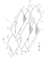
- FIG. 1 is a diagram for explaining a principle of operation of a wireless power transmission system 1 of an embodiment of the present disclosure. As shown in this diagram, the wireless power transmission system 1 includes a power transmitting device 10 and a power receiving device 20.
- the power transmitting device 10 includes electrodes 11 and 12, inductors 13 and 14, connection lines 15 and 16, and an AC (alternating current) power generating section 17.
- the power receiving device 20 includes electrodes 21 and 22, inductors 23 and 24, connection lines 25 and 26, and a load 27.
- the electrodes 11, 12 and the inductors 13, 14 constitute a power transmission coupler.
- the electrodes 21, 22 and the inductors 23, 24 constitute a power reception coupler.
- the electrodes 11, 12 are constituted by members having conductivity and are disposed across a predetermined distance d1.
- the electrodes 11, 12, 21 and 22 are exemplified by flat plate electrodes having a rectangle shape of substantially the same size.
- the electrode 11 and the electrode 21 are disposed in parallel and opposing each other across a distance d2, and the electrode 12 and the electrode 22 are disposed in parallel and opposing each other across the same distance d2.
- the electrodes 11, 12, 21 and 22 may be electrodes having a shape other than the shape shown in FIG. 1 .
- electrodes having, for example, shapes described below can be used.
- electrodes 201 and 202 having a substantially circular shape as shown in FIG. 2B
- electrodes 203 and 204 having a substantially elliptical shape as shown in FIG. 2C
- flat plate electrodes 205, 206, 207 and 208 having a substantially diamond shape as shown in FIGS. 2D and 2E
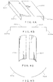
- electrodes 209 and 210 having a substantially prismatic shape as shown in FIG. 3A
- electrodes 211 and 212 having only outer shell portions 211b and 212b, respectively, in which substantially prismatic inner portions 211a and 212a are hollow as shown in FIG. 3B
- electrodes 213 and 214 having substantially a spherical shape as shown in FIG.
- electrodes 215 and 216 having only outer shell portions 215b and 216b, respectively, in which substantially spherical inner portions 215a and 216a are hollow as shown in FIG. 3D
- electrodes 217 and 218 having substantially a cylindrical shape as shown in FIG. 3E
- electrodes 219 and 220 having only outer shell portions 219b and 220b, respectively, in which substantially cylindrical inner portions 219a and 220a are hollow as shown in FIG. 3F .
- electrodes 223 and 224 having a curved shape as shown in a perspective view of FIG. 4C and a cross sectional view of FIG. 4D .
- a total width D of the electrodes 11 and 12 including a distance d1 is set so as to be narrower than a near field represented by ⁇ /2 ⁇ , where a wavelength of an electric field emitted by these electrodes is A.
- a total width D of the electrodes 21 and 22 including a distance d1 is set so as be narrower than a near field represented by ⁇ /2 ⁇ .
- a length L of the electrodes 11 and 12 is also set so as to be narrower than the near field represented by ⁇ /2 ⁇ .
- a length L of the electrodes 21 and 22 is also set so as to be narrower than the near field represent by ⁇ /2 ⁇ .
- a distance d2 between the electrode 11 and the electrode 21 and between the electrode 12 and the electrode 22 is also set so as to be shorter than the near field represented by ⁇ /2 ⁇ .
- the inductors 13 and 14 are configured as, for example, windings of an electrically-conductive wire rod (e.g., a copper wire), and, in the example of FIG. 1 , one end of each of the inductors 13 and 14 is electrically connected to an end portion of each of the electrodes 11 and 12.
- the connection line 15 is an electrically-conductive wire rod (e.g., a copper wire) that connects another end of the inductor 13 with one end of an output terminal of an AC power generating section 17.
- the connection line 16 is constituted by an electrically-conductive wire rod that connects another end of the inductor 14 with another end of the output terminal of the AC power generating section 17.
- the connection lines 15 and 16 are constituted by coaxial cables or balanced cables.
- the AC power generating section 17 produces an alternating-current power of a predetermined frequency and supplies it to the inductors 13 and 14 through the connection lines 15 and 16.
- the electrodes 21, 22 are constituted by members having conductivity and are disposed across a predetermined distance d1.
- the inductors 23 and 24 are configured as, for example, windings of an electrically-conductive wire rod, and, in the example of FIG. 1 , one end of each of the inductors 23 and 24 is electrically connected to an end portion of each of the electrodes 21 and 22.
- the connection line 25 is an electrically-conductive wire rod (e.g., a copper wire) that connects another end of the inductor 13 with one end of an input terminal of a load 27.
- the connection line 26 is constituted by an electrically-conductive wire rod that connects another end of the inductor 24 with another end of the input terminal of the load 27.
- the connection lines 25 and 26 are constituted by coaxial cables or balanced cables.
- the load 27 is supplied with electric power which is output from the AC power generating section 17 and transmitted through a power transmission coupler and a power reception coupler.
- the load 27 is, for example, constituted by a rectifier and secondary battery, or the like. Of course, it may be other than this.
- FIG. 5 is a diagram showing an equivalent circuit of the wireless power transmission system 1 shown in FIG. 1 .
- impedance 2 represents a characteristic impedance of the connection lines 15, 16 and the connection lines 25, 26, and has a value of Z0.
- An inductor 3 corresponds to the inductors 13, 14, and has an element value of L.
- a capacitor 4 has an element value (C-Cm) obtained by subtracting an element value Cm of a capacitor produced between the electrodes 11, 12 and the electrodes 21, 22 from an element value C of a capacitor produced between the electrodes 11 and 12.
- a capacitor 5 represents a capacitor produced between the electrodes 11, 12 and the electrodes 21, 22, and has an element value of Cm.
- a capacitor 6 has an element value (C-Cm) obtained by subtracting an element value Cm of a capacitor produced between the electrodes 11, 12 and the electrodes 21, 22 from an element value C of a capacitor produced between the electrodes 21 and 22.
- An inductor 7 corresponds to the inductors 23 and 24, and has an element value of L.
- FIG. 6 shows frequency characteristics of an S parameter between the power transmitting device 10 and the power receiving device 20.
- a horizontal axis of FIG. 6 represents frequency and a vertical axis represents insertion loss (S21) from the power transmitting device 10 to the power receiving device 20.
- the insertion loss from the power transmitting device 10 to the power receiving device 20 has an antiresonance point at frequency fC and has resonance points at frequencies fL and fH.
- frequency fC is determined by inductance values L of the inductors 3, 7 shown in FIG. 5 and the capacitance values C of the capacitors formed by the electrodes 11 and 12 or the electrodes 21 and 22.
- the frequencies fL and fH are determined by the inductance values L of the inductors 3 and 7 shown in FIG. 5 , the capacitance value Cm of the capacitor formed by the electrodes 11, 12 and the electrodes 21, 22, as well as the capacitance value C of the capacitors produced between the electrodes 11, 12 and between the electrodes 21, 22, respectively.
- a frequency of an alternating-current power produced by the AC power generating section 17 is configured to be substantially equal to the resonance frequency of the power transmission coupler constituted by first and second electrodes 11 and 12 and the inductors 13 and 14.
- the capacitance value C is determined by a size, a shape and an arrangement of electrodes of each of the power transmission coupler and the power reception coupler.
- the capacitance value Cm depends on a distance d2 between the power transmission and reception electrodes in addition to the size, the shape and the arrangement of the electrodes of each coupler. Therefore, input impedance from the AC power generating section 17 side in the equivalent circuit of FIG. 5 varies depending on the size, the shape, and the arrangement of the electrodes and the distance between the power transmission and reception electrodes.
- the frequency of the alternating-current power produced by the AC power generating section 17 may be set to a frequency at which the transmission efficiency of the electric power from the power transmission coupler to the power reception coupler becomes maximum. By setting the frequency in such a manner, transmission efficiency can be maximized.
- the electrodes 11 and 12 of the power transmitting device 10 and the electrodes 21 and 22 of the power receiving device 20 are coupled with electric field resonance, and an alternating-current power is transmitted from the electrodes 11 and 12 of the power transmitting device 10 to the electrodes 21 and 22 of the power receiving device 20 using an electric field.
- the electrodes 11, 12 of the power transmitting device 10 and the electrodes 21, 22 of the power receiving device 20 are disposed across a distance d2 which is shorter than ⁇ /2 ⁇ which is a near field range, the electrodes 21 and 22 are disposed in a region where an electric field components emitted from the electrodes 11 and 12 are dominant. Further, a resonance frequency due to the capacitor formed between the electrodes 11 and 12 and the inductors 13 and 14 and a resonance frequency due to the capacitor formed between the electrodes 21 and 22 and the inductors 23 and 24 are configured to be substantially equal.
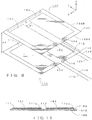
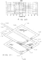
- FIGS. 7 and 8 are perspective views showing configuration examples of the embodiment of the present disclosure.
- FIG. 7 shows a configuration example of the power transmission coupler 110 of the embodiment.
- FIG. 8 is a perspective view showing a state where the power transmission coupler 110 and the power reception coupler 120 are arranged.
- the power transmission coupler 110 includes electrodes 111 and 112, which are conductive members having a rectangular shape, disposed on a front face 118A of a circuit board 118, which is an insulating member having a rectangular plate shape. In the example of FIG. 7 , no electrodes are disposed on a back face 118B of the circuit board 118.
- the electrodes 111 and 112 are formed on the circuit board 118 of a glass epoxy substrate or a glass composite substrate by an electrically-conductive film, such as copper.
- the electrodes 111 and 112 are disposed in parallel at positions spaced apart by a predetermined distance d1. Width D of the electrodes 111, 112 including a distance d1 is set so as to be narrower than a near field expressed as ⁇ /2 ⁇ , where A is a wavelength of an electric field emitted from the electrodes.
- each of the inductors 113, 114 is connected to an end portion in a shorter direction of the electrodes 111, 112 of the circuit board 118, respectively.
- the other ends of the inductors 113, 114 are connected to one ends of the connection lines 115, 116, respectively.
- the connection lines 115, 116 are disposed in such a manner that they avoid regions of the electrodes 111, 112 and a region interposed therebetween and are disposed in a direction (bottom right direction in FIG. 7 ) extending away from those regions.
- connection lines 115, 116 are, for example, constituted by coaxial cables or balanced cables. Note that the other end of each of the connection lines 115, 116 is connected to an output terminal of the AC power generating section, not to illustrate, respectively.
- the power transmitting device includes the AC power generating section connected to the power transmission coupler 110 via the connection lines 115, 116.
- the circuit board 118 does not need to be a rigid body, and, for example, may be a dielectric film such as polyimide. Since such a dielectric film has flexibility, an electrode portion can be rolled up or folded in accordion shape when not in use, and can improve ease of transportation and ease of store of the electrode portion.
- a dielectric film such as polyimide. Since such a dielectric film has flexibility, an electrode portion can be rolled up or folded in accordion shape when not in use, and can improve ease of transportation and ease of store of the electrode portion.
- the electrodes may be provided with rigidity and secured to a housing without a supporting substrate such as the circuit board 118.
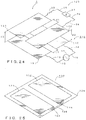
- FIG. 9 is a configuration example of the power transmission coupler 110, and the electrodes 111 and 112 are secured to dielectric supports 141 by screws 142.
- the dielectric support 141 is configured to be secured to a coupler installation housing, not shown, by a screw. With such a configuration shown in FIG. 9 , the dielectric supports 141 may be installed by a number capable of stably securing the electrodes 111, 112 to the housing. A similar configuration can be applied to a power receiving side coupler.
- a fin for dissipating heat may be disposed on the electrodes 111, 112 to dissipate heat during electric power transmission.
- the perspective view of FIG. 10A and the cross sectional view of FIG. 10B show an example in which a radiation fin 151 is provided which has an increased surface area by forming raised and recessed portions continuously in an in-plane direction on surfaces 111a, 112a of the electrodes 111, 112 of FIG. 7 .
- the heat produced can be dissipated from the radiation fin 151 provided on surfaces 111a, 112a of the electrodes 111, 112.
- FIG. 10C is an example in which, in a configuration of FIG. 9 , the radiation fin 151 is disposed on the surfaces 111a, 112a of the electrodes 111, 112, and the electrodes 111, 112 are secured to the dielectric supports 141 with screws 142, with which an effect similar to that of the configuration of FIG. 10A can be obtained.
- FIGS. 10A and 10C it is possible to provide the radiation fin 151 on back faces which are opposite the front faces 111a, 112a of the electrodes 111, 112.
- a coolant may be enclosed inside the electrodes 111 and 112.
- a coolant may be enclosed inside the electrodes 111 and 112.
- heat produced mainly due to an alternating-current resistance of the coils 113 and 114 during electric power transmission can be dispersed across an exposed surface of the electrodes 211, 212, 215, 216, 219 and 220 by convection of the coolant and can release heat from the exposed surface.
- FIG. 11 shows an example of a case in which a coating is applied on the surfaces 111a and 112a which are the exposed surfaces of the electrodes 111 and 112 in a configuration shown in FIG. 7 , and shows a cross-section of the circuit board 118 and the electrodes 111, 112.
- the surfaces 111a and 112a which are the exposed surfaces of the electrodes 111 and 112, are covered with an insulating film 161.
- a similar coating is also applicable to a configuration as shown in FIG. 9 in which there is no dielectric substrate, and an entirety of the exposed surfaces of the electrodes 111 and 112 may be coated with an insulating film. Also, in a case where the radiation fin 151 shown in FIGS.
- the electrodes 111 and 112 a decrease in electric power transmission efficiency due to the corrosion of the electrodes 111, 112 can be suppressed by coating, with an insulating film, a portion where the electrodes 111 and 112 are exposed by extending beyond the radiation fin 151 or by coating, with an insulating film, the electrodes 111, 112 and the radiation fin 151 as a whole.
- the electrodes 111, 112 By coating the electrodes 111, 112 with the insulating film 161, even if a high voltage is applied between the electrodes 111 and 112, discharging from surfaces of the electrodes 111 and 112 can be suppressed.
- the electrodes can be coated with an insulating film even if they have a three dimensional structure as shown in FIG. 3A to FIG. 3F .
- the power transmission coupler 110 constitutes a series resonant circuit with a capacitance C of a capacitor formed by the electrodes 111 and 112 disposed across a predetermined distance d1 and an inductance L of the inductors 113 and 114, and thus has a natural resonance frequency fC based on them.
- the power reception coupler 120 has a configuration similar to the power transmission coupler 110, in which electrodes 121 and 122, which are conductive members having a rectangular shape, disposed on a front face 128A of a circuit board 128, and connection lines 125 and 126 are connected to the another ends of the inductors 123 and 124.
- Resonance frequency fC of a series resonant circuit by capacitance C of the capacitor formed by the electrodes 121 and 122 and inductance L of the inductors 123 and 124 is substantially the same as that of the power transmission coupler 110.
- the connection lines 125 and 126 are, for example, constituted by coaxial cables or balanced cables.
- a load not shown, is connected to the other end of the connection lines 125 and 126 of the power reception coupler 120.
- the power receiving device includes a load connected to the power reception coupler 120 via the connection lines 125, 126.
- FIG. 8 is a diagram showing a state where the power transmission coupler 110 and the power reception coupler 120 are disposed opposing each other. As shown in this diagram, the power transmission coupler 110 and the power reception coupler 120 are disposed across a distance d2 in such a manner that the front faces 118A, 128A of the circuit boards 118, 128 oppose each other and the circuit boards 118 and 128 are parallel to each other.
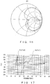
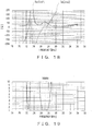
- 2 ) from the power transmission coupler 110 to the power reception coupler 120 in a case where the power transmission coupler 110 and the power reception coupler 120 of the embodiment shown in FIG. 8 are disposed opposing each other at an interval of 14 cm (a case where d2 14 cm).
- a horizontal axis represents a frequency (MHz) of a alternating-current power to be transmitted and a vertical axis represents transmission efficiency.
- transmission efficiency of greater than or equal to 80% is achieved around 25 MHz.
- a solid line represents a frequency characteristic of an absolute value of the parameter S21
- a broken line represents a frequency characteristic of an absolute value of the parameter S11.
- the parameter S11 represents reflection of a signal inputted from the power transmission coupler 110
- the parameter S21 represents passage of a signal from the power transmission coupler 110 to the power reception coupler 120.
- 2 ) from the power transmission coupler 110 to the power reception coupler 120 in a case where the power transmission coupler 110 and the power reception coupler 120 are disposed opposing each other at an interval of 17 cm (a case where d2 17 cm). As shown in this graph, it can be seen that, when the frequency is near 27 MHz, transmission efficiency is around 80%.
- a port impedance of a measuring device is set at a value equal to a characteristic impedance Z0 (real number) of the connection line.
- Z0 real number
- each of the impedances is substantially zero near 27 MHz, which is a resonance frequency, it can be seen that an electric power can be transmitted from the power transmission coupler 110 to the power reception coupler 120 with a reduced loss.
- VSWR voltage standing-wave ratios
- the voltage standing-wave ratios of the power transmission coupler 110 and the power reception coupler 120 are substantially 1 near 27 MHz, which is a resonance frequency, impedance is matched from an AC power generating section, not shown, to the power transmission coupler 110 to the power reception coupler 120, or from the power reception coupler 120 to a load, not shown, and it can be seen that an electric power can be transmitted without reflection.
- the power transmission coupler 110 and the power reception coupler 120 are disposed at an interval of, for example, about 17 cm, since transmission efficiency of around 80% can be achieved, an electric power can be transmitted efficiently. Also, it can be seen that, at the resonance frequency, a resistance component of the impedance becomes substantially 0, and that there is less reflection.
- connection lines 115, 116 and the connection lines 125, 126 are disposed to avoid regions of the electrodes 111, 112 and the electrodes 121, 122 and a region interposed between these regions, and, for example, as shown in FIG. 21 , in a case where the region (the region interposed between the electrodes 111, 112 and the electrodes 121, 122 in an example of FIG. 21 ) is not avoided and disposed so as to pass through the region, transmission characteristic deteriorates as shown in FIGS. 22 and 23 .
- connection lines 115 and 116 are disposed in a region interposed between the electrodes 111 and 112
- connection lines 125 and 126 are disposed in a region interposed between the electrodes 121 and 122 as shown in FIG. 21
- characteristics shown in FIG. 22 (characteristics in a case where they are disposed as shown in FIG. 8 ) deteriorates as shown in FIG. 23
- the transmission characteristic at a peak decreases from about 0.8 to 0.7.
- connection lines 115 and 116 are disposed to pass directly above or in the vicinity of the electrodes 111, 112, the transmission characteristics deteriorate in a similar to the case of FIG. 21 . Therefore, it is desirable that the connection lines 115 and 116 are disposed at positions separate from the electrodes 111, 112, and disposed to extend in a direction away from them. Of course, the connection lines 125 and 126 are disposed in a similar manner.
- connection lines 115, 116 and the connection lines 125, 126 can be facilitated. Also, with such an arrangement, since the connection lines 115, 116 and the connection lines 125, 126 can be disposed at positions separate from the electrodes 111, 112 and the electrodes 121, 122, a decrease in transmission efficiency can be prevented.
- the inductors 123, 124 may be disposed at a region interposed between the electrodes 111, 112 and the electrodes 121, 122, and the connection line 115, 116 and the connection line 125, 126 may extend in a direction normal to the circuit board 118 and the circuit board 128.
- the electrodes 111, 112 and the electrodes 121, 122 are of the same size, but these may be of different sizes.
- the electrodes 121, 122 may be of a size smaller than the size of the electrodes 111, 112.
- an opposite configuration may be employed.
- the electrodes 111, 112 and the electrodes 121, 122 are disposed opposing each other, but, for example, these may be disposed in a state displaced in an X-direction or a Y-direction shown in FIG. 8 .
- the power transmission coupler 110 and the power reception coupler 120 may be arranged in such a manner that they are rotated through a predetermined angle with respect to each other. In such a case, as shown in FIG.
- the shape of the electrodes 111, 112 and the electrodes 121, 122 need not be a rectangular shape.
- the electrodes 111, 112 and the electrodes 121, 122 may be flat plate electrodes having a circular shape, an elliptical shape or a diamond shape as shown in FIGS. 2A to 2E , or a prism, a sphere, a cylinder, or a three-dimensional shape having only an outer shell portion thereof as shown in FIGS. 3A to 3F , and alternatively, electrodes having a shape that is not a simple flat plate but a curved shape or bent shape obtained from a flat plate as shown in FIGS. 4A to 4D .
- the configuration includes two electrodes disposed at a certain distance to form a capacitor, there is no essential difference in a principle of operation of electric power transmission as compared to the case of the electrode structure shown in FIG. 1 and thus it is applicable to the present disclosure.
- the inductors 113, 114 and the inductors 123, 124 are interposed between the electrodes 111, 112 and the electrodes 121, 122 and the connection lines 115, 116 and the connection lines 125, 126, but it is possible to interpose them at positions other than such positions (e.g., in the vicinity of the AC power generating section or in the vicinity of the load).
- the power transmission coupler 110 and the power reception coupler 120 are provided with two each of the inductors 113, 114 and the inductors 123, 124, respectively, but may be each provided with a single inductor.
- an inductor was configured as a conductor wire which is wound cylindrically, but may be, for example, configured as a shape meandering on a plane or a spiral shape on a plane such as those used in a microstripline.
- an inductor may be formed integral with the electrodes 111, 112 on the circuit board 118 or on a film.
- a coupler can be rolled up or folded in an accordion manner when not in use, and it is possible to increase transportation property and storing property of the coupler.
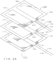
- the configuration includes the power transmission coupler 110 and the power reception coupler 120, but may be a configuration that has a relay coupler 130 as shown in FIG. 25 .
- the relay coupler 130 shown in FIG. 25 is configured such that other ends of the inductors 133, 134 of the coupler having a configuration similar to FIG. 7 are connected with each other by the connection line 135.
- these inductors 133, 134 may be configured as a single inductor.
- a resonance frequency fC of the relay coupler 130 is set to be substantially the same as those of the power transmission coupler 110 and the power reception coupler 120.
- FIG. 26 shows a configuration example of the wireless power transmission system using such a relay coupler 130.
- the relay coupler 130 is disposed between the power transmission coupler 110 and the power reception coupler 120 so as to be parallel to the two couplers. According to such a configuration, electric power can be transmitted through a greater distance and more efficiently as compared to a case in which the relay coupler 130 is not used.
- FIG. 27 shows a configuration in which, in the configuration shown in FIG.
- FIG. 28 shows a configuration in which, in configuration shown in FIG. 1 , each electrode is opposed in an order of all electrodes 11, 12, 21 and 22 while being superimposed spatially.
- electric power can be transmitted from the power transmitting side to the power receiving side through an electric field produced between the electrodes similarly to the configuration shown in FIG. 1 .
- FIG. 29 shows a configuration in which, in the configuration shown in FIG. 1 , electrodes 11, 12 of a curved shape are opposed to form a tubular structure 230, electrodes 21, 22 of a curved shape are opposed to form a tubular structure 240, and these structures are disposed substantially concentrically by inserting the tubular structure 230 inside the tubular structure 240. Also, in the configuration shown in FIG. 29 , a slit 231 separating the electrodes 11 and 12 of the power transmitting side coupler and a slit 241 separating the electrodes 21 and 22 of the power receiving side coupler are opposed to ensure the coupling of the electric field.
- Such a configuration shown in FIG. 29 may be used in applications such as an arm or a joint of a robot since electric power can be transmitted even if the coupler is slid in an axial direction.
- a coupling capacity between the couplers changes by sliding the tubular structure 240 with respect to the tubular structure 230 in an axial direction
- the input impedance can be adjusted.
- a length in an axial direction of the tubular structure 230 of the power transmitting side coupler and the tubular structure 240 of the power receiving side coupler smaller, since a relative slide in the axial direction of the coupler having a reduced length does not cause a change in the coupling capacity of the couplers, it may be used in applications such as performing electric power transmission of a fixed quantity in a sliding mechanism system. Note that it is not limited to the configuration shown in FIG. 29 , and, as long as both tubular structures of the power transmitting side and the power receiving side are disposed substantially concentrically, for example, the tubular structure of the power receiving side may be inserted inside the tubular structure of the power transmitting side.
- FIG. 30 shows a configuration in which, in the configuration shown in FIG. 1 , the electrodes 21, 22 each having a tubular shape of a diameter smaller than a diameter of the electrodes 11, 12 are disposed concentrically in the electrodes 11, 12 having a tubular shape. Also, in the configuration shown in FIG. 30 , a slit 231 separating the electrodes 11 and 12 of the power transmitting side coupler and a slit 241 separating the electrodes 21 and 22 of the power receiving side coupler are opposed from a point of view of ensuring the coupling of the electric field. Further, in the configuration shown in FIG.
- the electrodes 21, 22 on the power receiving side have diameters smaller than those of the electrodes 11, 12 of the power transmitting side, but it is not limited thereto, and a diameter of the electrodes on the power transmitting side may be made smaller than that of the power receiving side, and the electrodes on the power transmitting side may be placed in the electrodes of the power receiving side in a concentric manner.
- the electrode configuration exemplified in FIGS. 27 to 30 described above is a configuration in which the electrodes 11, 12 of the power transmitting side and the electrodes 21, 22 of the power receiving side have a constant distance and respectively form a capacitor, and there is no essential difference between the electrode configuration shown in FIG. 1 and the principle of operation during electric power transmission. Also, in any configuration exemplified in FIGS. 27 to 30 , similarly to the electrode configuration shown in FIG. 1 , conditions on an electrode size of the power transmitting side and the power receiving side may be made different.
Landscapes
- Engineering & Computer Science (AREA)
- Power Engineering (AREA)
- Computer Networks & Wireless Communication (AREA)
- Signal Processing (AREA)
- Charge And Discharge Circuits For Batteries Or The Like (AREA)
Claims (12)
- Drahtloses Stromübertragungssystem, das Wechselstrom von einer Stromsendevorrichtung (10) zu einer Stromempfangsvorrichtung (20) drahtlos überträgt, wobei das drahtlose Stromübertragungssystem aufweist:die Stromsendevorrichtung (10), welche enthält:erste und zweite Elektroden (11, 12), die mit einem vorbestimmten Abstand voneinander angeordnet sind, wobei die ersten und zweiten Elektroden (11, 12) eine den vorbestimmten Abstand enthaltende Gesamtbreite von weniger als oder gleich λ/2π haben, was ein Nahfeldbereich ist;erste und zweite Verbindungsleitungen (15, 16), die die ersten und zweiten Elektroden (11, 12) jeweils mit zwei Ausgangsanschlüssen eines Wechselstromerzeugungsabschnitts (17) elektrisch verbinden; undzumindest einen ersten Induktor (13, 14), der zwischen den ersten und zweiten Elektroden (11, 12) und zumindest einem der zwei Ausgangsanschlüsse des Wechselstromerzeugungsabschnitts (17) eingefügt ist,die Stromempfangsvorrichtung (20), welche enthält:dritte und vierte Elektroden (21, 22), die mit einem vorbestimmten Abstand voneinander angeordnet sind, wobei die dritten und vierten Elektroden (21, 22) eine den vorbestimmten Abstand enthaltende Gesamtbreite von weniger als oder gleich λ/2π haben, was ein Nahfeldbereich ist;dritte und vierte Verbindungsleitungen (25, 26), die die dritten und vierten Elektroden (21, 22) jeweils mit zwei Eingangsanschlüssen einer Last (27) elektrisch verbinden; undzumindest einen zweiten Induktor (23, 24), der zwischen die dritten und vierten Elektroden (21, 22) und zumindest einem der zwei Eingangsanschlüsse der Last (27) eingefügt ist,wobei ein Koppler, der die ersten und zweiten Elektroden (11, 12) und den zumindest einen ersten Induktor (13, 14) enthält, einen Schwingkreis bildet, und ein Koppler, der die dritten und vierten Elektroden (21, 22) und den zumindest einen zweiten Induktor (23, 24) enthält, einen anderen Schwingkreis bildet,wobei eine Resonanzfrequenz des Kopplers, der die ersten und zweiten Elektroden (11, 12) und den zumindest einen ersten Induktor (13, 14) enthält, und eine Resonanzfrequenz des Kopplers, der die dritten und vierten Elektroden (21, 22) und den zumindest einen zweiten Induktor (23, 24) enthält, im Wesentlichen gleich konfiguriert sind, wobei die ersten und zweiten Elektroden (11, 12) und die dritten und vierten Elektroden (21, 22) mit einem Abstand voneinander angeordnet sind, der kleiner als oder gleich λ/2π ist, was ein Nahfeldbereich ist, wobei λ eine Wellenlänge eines von den Elektroden (11, 12, 21, 22) abgegebenen elektrischen Felds ist,wobei Wechselstrom von der Stromsendevorrichtung (10) zu der Stromempfangsvorrichtung (20) mittels elektrischer Feldresonanz übertragen wird, dadurch gekennzeichnet, dass die ersten bis vierten Elektroden (11, 12, 21, 22) eine flache Plattenform haben und die ersten und zweiten Elektroden (11, 12) und die dritten und vierten Elektroden (21, 22) jeweils in der gleichen Ebene angeordnet sind.
- Das drahtlose Stromübertragungssystem nach Anspruch 1, wobei die ersten und dritten Elektroden (11, 21) und die zweiten und vierten Elektroden (12, 22) parallel angeordnet sind.
- Das drahtlose Stromübertragungssystem nach einem der Ansprüche 1 und 2, wobei die ersten und zweiten Verbindungsleitungen (15, 16) derart angeordnet sind, dass Bereiche der ersten und zweiten Elektroden (11, 12) und ein dazwischen eingefügter Bereich vermieden werden, und sich in Richtung von den Bereichen weg erstrecken.
- Das drahtlose Stromübertragungssystem nach einem der Ansprüche 1 bis 3, wobei die dritten und vierten Verbindungsleitungen (25, 26) derart angeordnet sind, dass Bereiche der dritten und vierten Elektroden (21, 22) und ein dazwischen eingefügter Bereich vermieden werden, und sich in Richtung von den Bereichen weg erstrecken.
- Das drahtlose Stromübertragungssystem nach einem der Ansprüche 1 bis 4, das ferner aufweist:eine Übermittlungsvorrichtung (130), welche enthält:fünfte und sechste Elektroden (131, 132), die mit einem vorbestimmten Abstand voneinander angeordnet sind, wobei die fünften und sechsten Elektroden (131, 132) eine den vorbestimmten Abstand enthaltende Gesamtbreite von weniger als oder gleich λ/2π haben, was ein Nahfeldbereich ist; undeinen dritten Induktor (133, 134), der zwischen den fünften und sechsten Elektroden (131, 132) angeschlossen ist,wobei die fünften und sechsten Elektroden (131, 132) zwischen den ersten und zweiten Elektroden (11, 12) der Stromsendevorrichtung (10) und den dritten und vierten Elektroden (21, 22) der Stromempfangsvorrichtung (20) angeordnet sind,wobei eine Resonanzfrequenz eines Kopplers, der die fünften und sechsten Elektroden (131, 132) und den dritten Induktor (133, 134) enthält, und eine Resonanzfrequenz von Kopplern der Stromsendevorrichtung (10) und der Stromempfangsvorrichtung (20) im Wesentlichen gleich konfiguriert sind.
- Drahtloses Stromübertragungssystem, das Wechselstrom von einer Stromsendevorrichtung (10) zu einer Stromempfangsvorrichtung (20) drahtlos überträgt, wobei das drahtlose Stromübertragungssystem aufweist:die Stromsendevorrichtung (10), welche enthält:erste und zweite Elektroden (11, 12), die mit einem vorbestimmten Abstand voneinander angeordnet sind, wobei die ersten und zweiten Elektroden (11, 12) eine den vorbestimmten Abstand enthaltende Gesamtbreite von weniger als oder gleich λ/2π haben, was ein Nahfeldbereich ist;erste und zweite Verbindungsleitungen (15, 16), die die ersten und zweiten Elektroden (11, 12) jeweils mit zwei Ausgangsanschlüssen eines Wechselstromerzeugungsabschnitts (17) elektrisch verbinden; undzumindest einen ersten Induktor (13, 14), der zwischen den ersten und zweiten Elektroden (11, 12) und zumindest einem der zwei Ausgangsanschlüsse des Wechselstromerzeugungsabschnitts (17) eingefügt ist,die Stromempfangsvorrichtung (20), welche enthält:dritte und vierte Elektroden (21, 22), die mit einem vorbestimmten Abstand voneinander angeordnet sind, wobei die dritten und vierten Elektroden (21, 22) eine den vorbestimmten Abstand enthaltende Gesamtbreite von weniger als oder gleich λ/2π haben, was ein Nahfeldbereich ist;dritte und vierte Verbindungsleitungen (25, 26), die die dritten und vierten Elektroden (21, 22) jeweils mit zwei Eingangsanschlüssen einer Last (27) elektrisch verbinden; undzumindest einen zweiten Induktor (23, 24), der zwischen die dritten und vierten Elektroden (21, 22) und zumindest einem der zwei Eingangsanschlüsse der Last (27) eingefügt ist,wobei ein Koppler, der die ersten und zweiten Elektroden (11, 12) und den zumindest einen ersten Induktor (13, 14) enthält, einen Schwingkreis bildet, und ein Koppler, der die dritten und vierten Elektroden (21, 22) und den zumindest einen zweiten Induktor (23, 24) enthält, einen anderen Schwingkreis bildet,wobei eine Resonanzfrequenz des Kopplers, der die ersten und zweiten Elektroden (11, 12) und den zumindest einen ersten Induktor (13, 14) enthält, und eine Resonanzfrequenz des Kopplers, der die dritten und vierten Elektroden (21, 22) und den zumindest einen zweiten Induktor (23, 24) enthält, im Wesentlichen gleich konfiguriert sind, wobei die ersten und zweiten Elektroden (11, 12) und die dritten und vierten Elektroden (21, 22) mit einem Abstand voneinander angeordnet sind, der kleiner als oder gleich λ/2π ist, was ein Nahfeldbereich ist, wobei λ eine Wellenlänge eines von den Elektroden (11, 12, 21, 22) abgegebenen elektrischen Felds ist,wobei Wechselstrom von der Stromsendevorrichtung (10) zu der Stromempfangsvorrichtung (20) mittels elektrischer Feldresonanz übertragen wird,wobei die ersten und zweiten Elektroden (11, 12) eine gekrümmte Form haben und zur Bildung einer ersten rohrförmigen Struktur einander gegenüberliegen, wobei ein Außenumfang der ersten rohrförmigen Struktur eine Länge von weniger als oder gleich λ/2π hat, was ein Nahfeldbereich ist;wobei die dritten und vierten Elektroden (21, 22) eine gekrümmte Form haben und zur Bildung einer zweiten rohrförmigen Struktur einander gegenüberliegen, wobei ein Außenumfang der zweiten rohrförmigen Struktur eine Länge von weniger als oder gleich λ/2π hat, was ein Nahfeldbereich ist; undwobei die ersten und zweiten rohrförmigen Strukturen im Wesentlichen konzentrisch angeordnet sind, derart, dass ein die ersten und zweiten Elektroden (11, 12) trennender Schlitz und ein die dritten und vierten Elektroden (21, 22) trennender Schlitz einander gegenüberliegen.
- Das drahtlose Stromübertragungssystem nach einem der Ansprüche 1 bis 6, wobei eine Frequenz der Wechselstromerzeugungsabschnitts (17) im Wesentlichen auf die gleiche Frequenz wie eine Resonanzfrequenz des Kopplers, der die ersten und zweiten Elektroden (11, 12) und den zumindest einen ersten Induktor (13, 14) enthält, gesetzt ist.
- Das drahtlose Stromübertragungssystem nach einem der Ansprüche 1 bis 7, wobei eine Frequenz des Wechselstromerzeugungsabschnitts (17) auf eine Frequenz gesetzt ist, bei der eine Stromübertragungseffizienz von der Stromsendevorrichtung (10) zu der Stromempfangsvorrichtung (20) maximal ist.
- Das drahtlose Stromübertragungssystem nach einem der Ansprüche 1 bis 8, wobeider zumindest eine erste Induktor (13, 14) zwei Induktoren (13, 14) enthält, die ein Induktor (13), der zwischen die erste Elektrode (11) und die erste Verbindungsleitung (15) eingefügt ist, und ein zweiter Induktor (14), der zwischen die zweite Elektrode (12) und die zweite Verbindungsleitung (16) eingefügt ist, sind, undder zumindest eine zweite Induktor (23, 24) zwei Induktoren (23, 24) enthält, die ein Induktor (23), der zwischen die dritte Elektrode (21) und die dritte Verbindungsleitung (25) eingefügt ist, und ein Induktor (24), der zwischen die vierte Elektrode (22) und die vierte Verbindungsleitungen (26) eingefügt ist, sind.
- Das drahtlose Stromübertragungssystem nach einem der Ansprüche 1 bis 9, wobeieine Isolierbeschichtung auf freiliegende Oberflächen der ersten und zweiten Elektroden (11, 12) aufgebracht ist; undeine Isolierbeschichtung auf freiliegende Oberflächen der dritten und vierten Elektroden (13, 14) aufgebracht ist.
- Stromsendevorrichtung in einem drahtlosen Stromübertragungssystem, das Wechselstrom von einer Stromsendevorrichtung (10) zu einer Stromempfangsvorrichtung (20) drahtlos überträgt, wobei sie aufweist:erste und zweite Elektroden (11, 12), die mit einem vorbestimmten Abstand voneinander angeordnet sind, wobei die ersten und zweiten Elektroden (11, 12) eine den vorbestimmten Abstand enthaltende Gesamtbreite von weniger als oder gleich λ/2π haben, was ein Nahfeldbereich ist;erste und zweite Verbindungsleitungen (15, 16), die die ersten und zweiten Elektroden (11, 12) jeweils mit zwei Ausgangsanschlüssen eines Wechselstromerzeugungsabschnitts (17) elektrisch verbinden; undzumindest einen ersten Induktor (13, 14), der zwischen den ersten und zweiten Elektroden (11, 12) und zumindest einem der zwei Ausgangsanschlüsse des Wechselstromerzeugungsabschnitts (17) eingefügt ist,wobei ein Koppler, der die ersten und zweiten Elektroden (11, 12) und den zumindest einen Induktor (13, 14) enthält, einen Schwingkreis bildet,wobei eine Resonanzfrequenz des Kopplers, der die ersten und zweiten Elektroden (11, 12) und den zumindest einen ersten Induktor (13, 14) enthält, im Wesentlichen gleich einer Resonanzfrequenz eines Kopplers der Stromempfangsvorrichtung (20) konfiguriert ist,wobei λ eine Wellenlänge eines von den Elektroden (11, 12) abgegebenen elektrischen Felds ist, wobei Wechselstrom von der Stromsendevorrichtung (10) zu der Stromempfangsvorrichtung (20) mittels elektrischer Feldresonanz übertragen wird, dadurch gekennzeichnet, dassdie ersten bis zweiten Elektroden (11, 12) eine flache Plattenform haben, und die ersten und zweiten Elektroden (11, 12) in der gleichen Ebene angeordnet sind.
- Stromempfangsvorrichtung für ein drahtloses Stromübertragungssystem, das Wechselstrom von einer Stromsendevorrichtung (10) an einer Stromempfangsvorrichtung (20) empfängt, wobei sie aufweist:dritte und vierte Elektroden (21, 22), die mit einem vorbestimmten Abstand voneinander angeordnet sind, wobei die dritten und vierten Elektroden (21, 22) eine den vorbestimmten Abstand enthaltende Gesamtbreite einer Dimension von weniger als oder gleich λ/2π haben, was ein Nahfeldbereich ist;dritte und vierte Verbindungsleitungen (25, 26), die die dritten und vierten Elektroden (21, 22) jeweils mit zwei Eingangsanschlüssen einer Last (27) elektrisch verbinden; undzumindest einen zweiten Induktor (23, 24), der zwischen die dritten und vierten Elektroden (21, 22) und zumindest einen der zwei Eingangsanschlüsse der Last (27) eingefügt ist,wobei ein Koppler, der die dritten und vierten Elektroden (21, 22) und den zumindest einen zweiten Induktor (23, 24) enthält, einen anderen Schwingkreis bildet,wobei eine Resonanzfrequenz des Kopplers, der die dritten und vierten Elektroden (21, 22) und den zumindest einen zweiten Induktor (23, 24) enthält, im Wesentlichen gleich einer Resonanzfrequenz eines Kopplers der Stromsendevorrichtung (10) konfiguriert ist, wobei λ eine Wellenlänge eines von der Stromsendevorrichtung (10) abgegebenen elektrischen Felds ist,wobei Wechselstrom von der Stromsendevorrichtung (10) an der Stromempfangsvorrichtung (20) mittels elektrischer Feldresonanz empfangen wird, dadurch gekennzeichnet, dass die dritten bis vierte Elektroden (21, 22) eine flache Plattenform haben, und die dritten und vierten Elektroden (21, 22) in der gleichen Ebene angeordnet sind.
Applications Claiming Priority (2)
| Application Number | Priority Date | Filing Date | Title |
|---|---|---|---|
| JP2012008037 | 2012-01-18 | ||
| PCT/JP2013/050982 WO2013108893A1 (ja) | 2012-01-18 | 2013-01-18 | 無線電力伝送システム、送電装置、および、受電装置 |
Publications (3)
| Publication Number | Publication Date |
|---|---|
| EP2806532A1 EP2806532A1 (de) | 2014-11-26 |
| EP2806532A4 EP2806532A4 (de) | 2015-10-28 |
| EP2806532B1 true EP2806532B1 (de) | 2020-06-17 |
Family
ID=48799314
Family Applications (1)
| Application Number | Title | Priority Date | Filing Date |
|---|---|---|---|
| EP13739121.5A Active EP2806532B1 (de) | 2012-01-18 | 2013-01-18 | Drahtloses stromübertragungssystem, stromübertragungsvorrichtung und stromempfangsvorrichtung |
Country Status (4)
| Country | Link |
|---|---|
| US (1) | US9824817B2 (de) |
| EP (1) | EP2806532B1 (de) |
| JP (1) | JP5603509B2 (de) |
| WO (1) | WO2013108893A1 (de) |
Families Citing this family (20)
| Publication number | Priority date | Publication date | Assignee | Title |
|---|---|---|---|---|
| SG11201400409XA (en) * | 2011-09-07 | 2014-04-28 | Solace Power Inc | Wireless electric field power transmission system and method |
| WO2014010044A1 (ja) * | 2012-07-11 | 2014-01-16 | 富士機械製造株式会社 | 静電結合方式非接触給電装置 |
| WO2014119194A1 (ja) * | 2013-01-31 | 2014-08-07 | 古河電気工業株式会社 | 無線電力伝送システム |
| JP6080158B2 (ja) * | 2013-01-31 | 2017-02-15 | 古河電気工業株式会社 | 無線電力伝送システム |
| JP2015082963A (ja) * | 2013-10-24 | 2015-04-27 | 古河電気工業株式会社 | ワイヤレス電力伝送システム |
| WO2015121054A1 (en) * | 2014-02-12 | 2015-08-20 | Koninklijke Philips N.V. | Illumination system comprising an array of leds |
| CA2953621A1 (en) * | 2014-06-26 | 2015-12-30 | Solace Power Inc. | Wireless electric field power transmission system, transmitter and receiver therefor and method of wirelessly transferring power |
| JP2016013042A (ja) * | 2014-06-30 | 2016-01-21 | 古河電気工業株式会社 | 電力伝送システム |
| WO2016033697A1 (en) | 2014-09-05 | 2016-03-10 | Solace Power Inc. | Wireless electric field power transfer system, method, transmitter and receiver therefor |
| JP2018107840A (ja) * | 2015-05-07 | 2018-07-05 | 株式会社ExH | 電力伝送回転体 |
| JP2017055605A (ja) * | 2015-09-10 | 2017-03-16 | 株式会社リューテック | ワイヤレス電力供給システム |
| US11228209B1 (en) * | 2017-08-02 | 2022-01-18 | Apple Inc. | Wireless power transfer system and method |
| WO2020142833A1 (en) | 2019-01-11 | 2020-07-16 | Solace Power Inc. | Wireless electric field power transfer system, transmitter and receiver |
| JP7358296B2 (ja) * | 2020-05-19 | 2023-10-10 | 新光電気工業株式会社 | 非接触給電装置 |
| CN112217290B (zh) * | 2020-10-15 | 2022-09-20 | 上海科技大学 | 一种用于电容耦合式无线能量传输的交叠型电容耦合器 |
| JP7693395B2 (ja) * | 2021-05-26 | 2025-06-17 | 古河電気工業株式会社 | 電力伝送システム、送電装置及び受電装置 |
| JP2022181285A (ja) * | 2021-05-26 | 2022-12-08 | 古河電気工業株式会社 | 電力伝送システム、送電装置、受電装置及び机 |
| JP7798332B2 (ja) * | 2021-11-08 | 2026-01-14 | 株式会社パワーウェーブ | 無線電力送信システム、送電装置、受電装置、及び移動体 |
| CN114759689B (zh) * | 2022-06-13 | 2022-09-27 | 中国科学院自动化研究所 | 无线供电装置 |
| WO2025099731A1 (en) * | 2023-11-12 | 2025-05-15 | Elssway Ltd. | Wireless power transfer system |
Citations (1)
| Publication number | Priority date | Publication date | Assignee | Title |
|---|---|---|---|---|
| WO2011148803A1 (ja) * | 2010-05-28 | 2011-12-01 | 株式会社村田製作所 | 電力伝送システム |
Family Cites Families (16)
| Publication number | Priority date | Publication date | Assignee | Title |
|---|---|---|---|---|
| JP3493537B2 (ja) | 1995-04-10 | 2004-02-03 | オムロン株式会社 | 無線電力伝送装置 |
| TWI295530B (en) | 2002-06-28 | 2008-04-01 | Canon Kk | Wireless communication apparatus and method |
| JP2004038254A (ja) * | 2002-06-28 | 2004-02-05 | Canon Inc | 無線通信機器及び無線通信方法 |
| JP2004348496A (ja) | 2003-05-23 | 2004-12-09 | Hitachi Ltd | 通信システム |
| JP2005079786A (ja) * | 2003-08-29 | 2005-03-24 | Sony Corp | 電力伝送システム,電力供給装置,電力受電装置,信号伝送システム,信号送信装置,および,信号受信装置。 |
| JP4893483B2 (ja) * | 2006-09-11 | 2012-03-07 | ソニー株式会社 | 通信システム |
| JP4605203B2 (ja) * | 2007-10-15 | 2011-01-05 | ソニー株式会社 | 通信システム並びに通信装置 |
| EP2234241A4 (de) * | 2007-12-04 | 2016-01-27 | Dyden Corp | Stromversorgungseinrichtung |
| JP4557049B2 (ja) * | 2008-06-09 | 2010-10-06 | ソニー株式会社 | 伝送システム、給電装置、受電装置、及び伝送方法 |
| US8278784B2 (en) * | 2008-07-28 | 2012-10-02 | Qualcomm Incorporated | Wireless power transmission for electronic devices |
| US8421274B2 (en) * | 2008-09-12 | 2013-04-16 | University Of Pittsburgh-Of The Commonwealth System Of Higher Education | Wireless energy transfer system |
| JP5354030B2 (ja) | 2009-06-25 | 2013-11-27 | 株式会社村田製作所 | 電力伝送システム及び非接触充電装置 |
| JP2011142724A (ja) * | 2010-01-06 | 2011-07-21 | Hitachi Ltd | 非接触電力伝送装置及びそのための近接場アンテナ |
| KR101761966B1 (ko) * | 2010-03-31 | 2017-07-26 | 가부시키가이샤 한도오따이 에네루기 켄큐쇼 | 전력 공급 장치와 그 구동 방법 |
| JP5824266B2 (ja) * | 2010-07-29 | 2015-11-25 | 株式会社半導体エネルギー研究所 | 半導体装置 |
| WO2014119194A1 (ja) * | 2013-01-31 | 2014-08-07 | 古河電気工業株式会社 | 無線電力伝送システム |
-
2013
- 2013-01-18 WO PCT/JP2013/050982 patent/WO2013108893A1/ja not_active Ceased
- 2013-01-18 EP EP13739121.5A patent/EP2806532B1/de active Active
- 2013-01-18 JP JP2013554363A patent/JP5603509B2/ja active Active
-
2014
- 2014-07-17 US US14/334,310 patent/US9824817B2/en active Active
Patent Citations (2)
| Publication number | Priority date | Publication date | Assignee | Title |
|---|---|---|---|---|
| WO2011148803A1 (ja) * | 2010-05-28 | 2011-12-01 | 株式会社村田製作所 | 電力伝送システム |
| US20120299392A1 (en) * | 2010-05-28 | 2012-11-29 | Keiichi Ichikawa | Power Transfer System |
Also Published As
| Publication number | Publication date |
|---|---|
| EP2806532A4 (de) | 2015-10-28 |
| WO2013108893A1 (ja) | 2013-07-25 |
| US9824817B2 (en) | 2017-11-21 |
| JP5603509B2 (ja) | 2014-10-08 |
| JPWO2013108893A1 (ja) | 2015-05-11 |
| US20140327321A1 (en) | 2014-11-06 |
| EP2806532A1 (de) | 2014-11-26 |
Similar Documents
| Publication | Publication Date | Title |
|---|---|---|
| EP2806532B1 (de) | Drahtloses stromübertragungssystem, stromübertragungsvorrichtung und stromempfangsvorrichtung | |
| US10158256B2 (en) | Contactless connector system tolerant of position displacement between transmitter coil and receiver coil and having high transmission efficiency | |
| JP6182551B2 (ja) | 無線電力伝送システム | |
| JP6080158B2 (ja) | 無線電力伝送システム | |
| CN103026436B (zh) | 具备散热构造的无线电力传输系统及送受电装置 | |
| JP5981202B2 (ja) | 電力伝送システム | |
| WO2014006895A1 (ja) | 無線電力伝送装置、無線電力送電装置および受電装置 | |
| CN102884711A (zh) | 用于在无线电力传输系统中控制谐振带宽的方法和设备 | |
| US9473212B2 (en) | Wireless power transmission system | |
| JP6301687B2 (ja) | 電力伝送システム | |
| US20200373786A1 (en) | A system and apparatus for wireless power transfer | |
| JP6088832B2 (ja) | 無線電力伝送システム | |
| JP5461277B2 (ja) | アンテナ装置、送電装置、受電装置および非接触電力伝送システム | |
| EP4589612A1 (de) | Leistungsübertragungsspuleneinheit | |
| JP6016654B2 (ja) | 無線電力伝送システム | |
| JP6116924B2 (ja) | 無線電力伝送システム | |
| JP2024017668A (ja) | インピーダンス変換装置 | |
| JP5465575B2 (ja) | 非接触電力伝送用アンテナ装置、送電装置、受電装置および非接触電力伝送システム |
Legal Events
| Date | Code | Title | Description |
|---|---|---|---|
| PUAI | Public reference made under article 153(3) epc to a published international application that has entered the european phase |
Free format text: ORIGINAL CODE: 0009012 |
|
| 17P | Request for examination filed |
Effective date: 20140805 |
|
| AK | Designated contracting states |
Kind code of ref document: A1 Designated state(s): AL AT BE BG CH CY CZ DE DK EE ES FI FR GB GR HR HU IE IS IT LI LT LU LV MC MK MT NL NO PL PT RO RS SE SI SK SM TR |
|
| DAX | Request for extension of the european patent (deleted) | ||
| RA4 | Supplementary search report drawn up and despatched (corrected) |
Effective date: 20150930 |
|
| RIC1 | Information provided on ipc code assigned before grant |
Ipc: H02J 17/00 20060101AFI20150924BHEP Ipc: H04B 5/00 20060101ALI20150924BHEP Ipc: H01F 38/14 20060101ALI20150924BHEP Ipc: H02J 7/02 20060101ALI20150924BHEP |
|
| STAA | Information on the status of an ep patent application or granted ep patent |
Free format text: STATUS: EXAMINATION IS IN PROGRESS |
|
| 17Q | First examination report despatched |
Effective date: 20181005 |
|
| REG | Reference to a national code |
Ref country code: DE Ref legal event code: R079 Ref document number: 602013069922 Country of ref document: DE Free format text: PREVIOUS MAIN CLASS: H02J0017000000 Ipc: H01F0038140000 |
|
| GRAP | Despatch of communication of intention to grant a patent |
Free format text: ORIGINAL CODE: EPIDOSNIGR1 |
|
| RIC1 | Information provided on ipc code assigned before grant |
Ipc: H02J 7/02 20160101ALI20191220BHEP Ipc: H04B 5/00 20060101ALI20191220BHEP Ipc: H01F 38/14 20060101AFI20191220BHEP |
|
| STAA | Information on the status of an ep patent application or granted ep patent |
Free format text: STATUS: GRANT OF PATENT IS INTENDED |
|
| INTG | Intention to grant announced |
Effective date: 20200130 |
|
| GRAS | Grant fee paid |
Free format text: ORIGINAL CODE: EPIDOSNIGR3 |
|
| GRAA | (expected) grant |
Free format text: ORIGINAL CODE: 0009210 |
|
| STAA | Information on the status of an ep patent application or granted ep patent |
Free format text: STATUS: THE PATENT HAS BEEN GRANTED |
|
| AK | Designated contracting states |
Kind code of ref document: B1 Designated state(s): AL AT BE BG CH CY CZ DE DK EE ES FI FR GB GR HR HU IE IS IT LI LT LU LV MC MK MT NL NO PL PT RO RS SE SI SK SM TR |
|
| REG | Reference to a national code |
Ref country code: GB Ref legal event code: FG4D |
|
| REG | Reference to a national code |
Ref country code: CH Ref legal event code: EP |
|
| REG | Reference to a national code |
Ref country code: DE Ref legal event code: R096 Ref document number: 602013069922 Country of ref document: DE |
|
| REG | Reference to a national code |
Ref country code: IE Ref legal event code: FG4D |
|
| REG | Reference to a national code |
Ref country code: AT Ref legal event code: REF Ref document number: 1282342 Country of ref document: AT Kind code of ref document: T Effective date: 20200715 |
|
| REG | Reference to a national code |
Ref country code: SE Ref legal event code: TRGR |
|
| REG | Reference to a national code |
Ref country code: SE Ref legal event code: TRGR |
|
| REG | Reference to a national code |
Ref country code: NO Ref legal event code: T2 Effective date: 20200617 |
|
| PG25 | Lapsed in a contracting state [announced via postgrant information from national office to epo] |
Ref country code: FI Free format text: LAPSE BECAUSE OF FAILURE TO SUBMIT A TRANSLATION OF THE DESCRIPTION OR TO PAY THE FEE WITHIN THE PRESCRIBED TIME-LIMIT Effective date: 20200617 Ref country code: GR Free format text: LAPSE BECAUSE OF FAILURE TO SUBMIT A TRANSLATION OF THE DESCRIPTION OR TO PAY THE FEE WITHIN THE PRESCRIBED TIME-LIMIT Effective date: 20200918 Ref country code: LT Free format text: LAPSE BECAUSE OF FAILURE TO SUBMIT A TRANSLATION OF THE DESCRIPTION OR TO PAY THE FEE WITHIN THE PRESCRIBED TIME-LIMIT Effective date: 20200617 |
|
| REG | Reference to a national code |
Ref country code: LT Ref legal event code: MG4D |
|
| REG | Reference to a national code |
Ref country code: NL Ref legal event code: MP Effective date: 20200617 |
|
| PG25 | Lapsed in a contracting state [announced via postgrant information from national office to epo] |
Ref country code: RS Free format text: LAPSE BECAUSE OF FAILURE TO SUBMIT A TRANSLATION OF THE DESCRIPTION OR TO PAY THE FEE WITHIN THE PRESCRIBED TIME-LIMIT Effective date: 20200617 Ref country code: BG Free format text: LAPSE BECAUSE OF FAILURE TO SUBMIT A TRANSLATION OF THE DESCRIPTION OR TO PAY THE FEE WITHIN THE PRESCRIBED TIME-LIMIT Effective date: 20200917 Ref country code: HR Free format text: LAPSE BECAUSE OF FAILURE TO SUBMIT A TRANSLATION OF THE DESCRIPTION OR TO PAY THE FEE WITHIN THE PRESCRIBED TIME-LIMIT Effective date: 20200617 Ref country code: LV Free format text: LAPSE BECAUSE OF FAILURE TO SUBMIT A TRANSLATION OF THE DESCRIPTION OR TO PAY THE FEE WITHIN THE PRESCRIBED TIME-LIMIT Effective date: 20200617 |
|
| REG | Reference to a national code |
Ref country code: AT Ref legal event code: MK05 Ref document number: 1282342 Country of ref document: AT Kind code of ref document: T Effective date: 20200617 |
|
| PG25 | Lapsed in a contracting state [announced via postgrant information from national office to epo] |
Ref country code: NL Free format text: LAPSE BECAUSE OF FAILURE TO SUBMIT A TRANSLATION OF THE DESCRIPTION OR TO PAY THE FEE WITHIN THE PRESCRIBED TIME-LIMIT Effective date: 20200617 Ref country code: AL Free format text: LAPSE BECAUSE OF FAILURE TO SUBMIT A TRANSLATION OF THE DESCRIPTION OR TO PAY THE FEE WITHIN THE PRESCRIBED TIME-LIMIT Effective date: 20200617 |
|
| PG25 | Lapsed in a contracting state [announced via postgrant information from national office to epo] |
Ref country code: SM Free format text: LAPSE BECAUSE OF FAILURE TO SUBMIT A TRANSLATION OF THE DESCRIPTION OR TO PAY THE FEE WITHIN THE PRESCRIBED TIME-LIMIT Effective date: 20200617 Ref country code: EE Free format text: LAPSE BECAUSE OF FAILURE TO SUBMIT A TRANSLATION OF THE DESCRIPTION OR TO PAY THE FEE WITHIN THE PRESCRIBED TIME-LIMIT Effective date: 20200617 Ref country code: AT Free format text: LAPSE BECAUSE OF FAILURE TO SUBMIT A TRANSLATION OF THE DESCRIPTION OR TO PAY THE FEE WITHIN THE PRESCRIBED TIME-LIMIT Effective date: 20200617 Ref country code: PT Free format text: LAPSE BECAUSE OF FAILURE TO SUBMIT A TRANSLATION OF THE DESCRIPTION OR TO PAY THE FEE WITHIN THE PRESCRIBED TIME-LIMIT Effective date: 20201019 Ref country code: ES Free format text: LAPSE BECAUSE OF FAILURE TO SUBMIT A TRANSLATION OF THE DESCRIPTION OR TO PAY THE FEE WITHIN THE PRESCRIBED TIME-LIMIT Effective date: 20200617 Ref country code: RO Free format text: LAPSE BECAUSE OF FAILURE TO SUBMIT A TRANSLATION OF THE DESCRIPTION OR TO PAY THE FEE WITHIN THE PRESCRIBED TIME-LIMIT Effective date: 20200617 Ref country code: CZ Free format text: LAPSE BECAUSE OF FAILURE TO SUBMIT A TRANSLATION OF THE DESCRIPTION OR TO PAY THE FEE WITHIN THE PRESCRIBED TIME-LIMIT Effective date: 20200617 Ref country code: IT Free format text: LAPSE BECAUSE OF FAILURE TO SUBMIT A TRANSLATION OF THE DESCRIPTION OR TO PAY THE FEE WITHIN THE PRESCRIBED TIME-LIMIT Effective date: 20200617 |
|
| PG25 | Lapsed in a contracting state [announced via postgrant information from national office to epo] |
Ref country code: IS Free format text: LAPSE BECAUSE OF FAILURE TO SUBMIT A TRANSLATION OF THE DESCRIPTION OR TO PAY THE FEE WITHIN THE PRESCRIBED TIME-LIMIT Effective date: 20201017 Ref country code: PL Free format text: LAPSE BECAUSE OF FAILURE TO SUBMIT A TRANSLATION OF THE DESCRIPTION OR TO PAY THE FEE WITHIN THE PRESCRIBED TIME-LIMIT Effective date: 20200617 Ref country code: SK Free format text: LAPSE BECAUSE OF FAILURE TO SUBMIT A TRANSLATION OF THE DESCRIPTION OR TO PAY THE FEE WITHIN THE PRESCRIBED TIME-LIMIT Effective date: 20200617 |
|
| REG | Reference to a national code |
Ref country code: DE Ref legal event code: R097 Ref document number: 602013069922 Country of ref document: DE |
|
| PLBE | No opposition filed within time limit |
Free format text: ORIGINAL CODE: 0009261 |
|
| STAA | Information on the status of an ep patent application or granted ep patent |
Free format text: STATUS: NO OPPOSITION FILED WITHIN TIME LIMIT |
|
| PG25 | Lapsed in a contracting state [announced via postgrant information from national office to epo] |
Ref country code: DK Free format text: LAPSE BECAUSE OF FAILURE TO SUBMIT A TRANSLATION OF THE DESCRIPTION OR TO PAY THE FEE WITHIN THE PRESCRIBED TIME-LIMIT Effective date: 20200617 |
|
| 26N | No opposition filed |
Effective date: 20210318 |
|
| PG25 | Lapsed in a contracting state [announced via postgrant information from national office to epo] |
Ref country code: SI Free format text: LAPSE BECAUSE OF FAILURE TO SUBMIT A TRANSLATION OF THE DESCRIPTION OR TO PAY THE FEE WITHIN THE PRESCRIBED TIME-LIMIT Effective date: 20200617 |
|
| PG25 | Lapsed in a contracting state [announced via postgrant information from national office to epo] |
Ref country code: MC Free format text: LAPSE BECAUSE OF FAILURE TO SUBMIT A TRANSLATION OF THE DESCRIPTION OR TO PAY THE FEE WITHIN THE PRESCRIBED TIME-LIMIT Effective date: 20200617 |
|
| REG | Reference to a national code |
Ref country code: CH Ref legal event code: PL |
|
| PG25 | Lapsed in a contracting state [announced via postgrant information from national office to epo] |
Ref country code: LU Free format text: LAPSE BECAUSE OF NON-PAYMENT OF DUE FEES Effective date: 20210118 |
|
| REG | Reference to a national code |
Ref country code: BE Ref legal event code: MM Effective date: 20210131 |
|
| PG25 | Lapsed in a contracting state [announced via postgrant information from national office to epo] |
Ref country code: LI Free format text: LAPSE BECAUSE OF NON-PAYMENT OF DUE FEES Effective date: 20210131 Ref country code: CH Free format text: LAPSE BECAUSE OF NON-PAYMENT OF DUE FEES Effective date: 20210131 |
|
| PG25 | Lapsed in a contracting state [announced via postgrant information from national office to epo] |
Ref country code: IE Free format text: LAPSE BECAUSE OF NON-PAYMENT OF DUE FEES Effective date: 20210118 |
|
| PG25 | Lapsed in a contracting state [announced via postgrant information from national office to epo] |
Ref country code: BE Free format text: LAPSE BECAUSE OF NON-PAYMENT OF DUE FEES Effective date: 20210131 |
|
| PG25 | Lapsed in a contracting state [announced via postgrant information from national office to epo] |
Ref country code: HU Free format text: LAPSE BECAUSE OF FAILURE TO SUBMIT A TRANSLATION OF THE DESCRIPTION OR TO PAY THE FEE WITHIN THE PRESCRIBED TIME-LIMIT; INVALID AB INITIO Effective date: 20130118 |
|
| P01 | Opt-out of the competence of the unified patent court (upc) registered |
Effective date: 20230512 |
|
| PG25 | Lapsed in a contracting state [announced via postgrant information from national office to epo] |
Ref country code: CY Free format text: LAPSE BECAUSE OF FAILURE TO SUBMIT A TRANSLATION OF THE DESCRIPTION OR TO PAY THE FEE WITHIN THE PRESCRIBED TIME-LIMIT Effective date: 20200617 |
|
| PG25 | Lapsed in a contracting state [announced via postgrant information from national office to epo] |
Ref country code: MK Free format text: LAPSE BECAUSE OF FAILURE TO SUBMIT A TRANSLATION OF THE DESCRIPTION OR TO PAY THE FEE WITHIN THE PRESCRIBED TIME-LIMIT Effective date: 20200617 |
|
| PG25 | Lapsed in a contracting state [announced via postgrant information from national office to epo] |
Ref country code: MT Free format text: LAPSE BECAUSE OF FAILURE TO SUBMIT A TRANSLATION OF THE DESCRIPTION OR TO PAY THE FEE WITHIN THE PRESCRIBED TIME-LIMIT Effective date: 20200617 |
|
| PG25 | Lapsed in a contracting state [announced via postgrant information from national office to epo] |
Ref country code: TR Free format text: LAPSE BECAUSE OF FAILURE TO SUBMIT A TRANSLATION OF THE DESCRIPTION OR TO PAY THE FEE WITHIN THE PRESCRIBED TIME-LIMIT Effective date: 20200617 |
|
| PGFP | Annual fee paid to national office [announced via postgrant information from national office to epo] |
Ref country code: GB Payment date: 20251127 Year of fee payment: 14 |
|
| PGFP | Annual fee paid to national office [announced via postgrant information from national office to epo] |
Ref country code: FR Payment date: 20251128 Year of fee payment: 14 |
|
| PGFP | Annual fee paid to national office [announced via postgrant information from national office to epo] |
Ref country code: SE Payment date: 20251210 Year of fee payment: 14 |
|
| PGFP | Annual fee paid to national office [announced via postgrant information from national office to epo] |
Ref country code: NO Payment date: 20260109 Year of fee payment: 14 Ref country code: DE Payment date: 20251203 Year of fee payment: 14 |