EP2807676B1 - Procédé de fabrication d'un contact électroconducteur sur une photopile - Google Patents
Procédé de fabrication d'un contact électroconducteur sur une photopile Download PDFInfo
- Publication number
- EP2807676B1 EP2807676B1 EP13701609.3A EP13701609A EP2807676B1 EP 2807676 B1 EP2807676 B1 EP 2807676B1 EP 13701609 A EP13701609 A EP 13701609A EP 2807676 B1 EP2807676 B1 EP 2807676B1
- Authority
- EP
- European Patent Office
- Prior art keywords
- adhesive
- solar cell
- connector
- region
- electrically conductive
- Prior art date
- Legal status (The legal status is an assumption and is not a legal conclusion. Google has not performed a legal analysis and makes no representation as to the accuracy of the status listed.)
- Active
Links
Images


Classifications
-
- H—ELECTRICITY
- H10—SEMICONDUCTOR DEVICES; ELECTRIC SOLID-STATE DEVICES NOT OTHERWISE PROVIDED FOR
- H10F—INORGANIC SEMICONDUCTOR DEVICES SENSITIVE TO INFRARED RADIATION, LIGHT, ELECTROMAGNETIC RADIATION OF SHORTER WAVELENGTH OR CORPUSCULAR RADIATION
- H10F71/00—Manufacture or treatment of devices covered by this subclass
- H10F71/137—Batch treatment of the devices
- H10F71/1375—Apparatus for automatic interconnection of photovoltaic cells in a module
-
- H—ELECTRICITY
- H10—SEMICONDUCTOR DEVICES; ELECTRIC SOLID-STATE DEVICES NOT OTHERWISE PROVIDED FOR
- H10F—INORGANIC SEMICONDUCTOR DEVICES SENSITIVE TO INFRARED RADIATION, LIGHT, ELECTROMAGNETIC RADIATION OF SHORTER WAVELENGTH OR CORPUSCULAR RADIATION
- H10F19/00—Integrated devices, or assemblies of multiple devices, comprising at least one photovoltaic cell covered by group H10F10/00, e.g. photovoltaic modules
- H10F19/90—Structures for connecting between photovoltaic cells, e.g. interconnections or insulating spacers
- H10F19/902—Structures for connecting between photovoltaic cells, e.g. interconnections or insulating spacers for series or parallel connection of photovoltaic cells
- H10F19/906—Structures for connecting between photovoltaic cells, e.g. interconnections or insulating spacers for series or parallel connection of photovoltaic cells characterised by the materials of the structures
-
- H—ELECTRICITY
- H10—SEMICONDUCTOR DEVICES; ELECTRIC SOLID-STATE DEVICES NOT OTHERWISE PROVIDED FOR
- H10F—INORGANIC SEMICONDUCTOR DEVICES SENSITIVE TO INFRARED RADIATION, LIGHT, ELECTROMAGNETIC RADIATION OF SHORTER WAVELENGTH OR CORPUSCULAR RADIATION
- H10F77/00—Constructional details of devices covered by this subclass
- H10F77/20—Electrodes
- H10F77/206—Electrodes for devices having potential barriers
- H10F77/211—Electrodes for devices having potential barriers for photovoltaic cells
-
- Y—GENERAL TAGGING OF NEW TECHNOLOGICAL DEVELOPMENTS; GENERAL TAGGING OF CROSS-SECTIONAL TECHNOLOGIES SPANNING OVER SEVERAL SECTIONS OF THE IPC; TECHNICAL SUBJECTS COVERED BY FORMER USPC CROSS-REFERENCE ART COLLECTIONS [XRACs] AND DIGESTS
- Y02—TECHNOLOGIES OR APPLICATIONS FOR MITIGATION OR ADAPTATION AGAINST CLIMATE CHANGE
- Y02E—REDUCTION OF GREENHOUSE GAS [GHG] EMISSIONS, RELATED TO ENERGY GENERATION, TRANSMISSION OR DISTRIBUTION
- Y02E10/00—Energy generation through renewable energy sources
- Y02E10/50—Photovoltaic [PV] energy
Definitions
- the invention relates to a method for producing an electrically conductive contact on a rear and / or front side of a solar cell, wherein the contact is connected to a solar cell interconnecting connector by means of an adhesive.
- the US 2008/0076307 A1 refers to a connection between a connector and a solar cell.
- the connector consists of a conductor and a surrounding z. B. electroplated layer.
- the connector may be provided with a conductive adhesive or solder material in the region where contact with the solar cell is made. It is also possible to apply to the area of the solar cell an adhesive or a solder material in which the contact with the connector is to be produced.
- a connection of solar cells to a solar cell module is the EP 2 056 355 A1 refer to.
- a busbar is first applied to the solar cell, which is then covered by an adhesive layer.
- a connector is applied under pressure with simultaneous application of heat, so that the connector partially surrounds the busbar.
- connection method for semiconductor chips is described in US patent application Ser US Pat. No. 7,264,991 B1 described. Between the semiconductor chip and the connector, an electrically conductive adhesive is provided to form a sandwich structure. Outside the compound, the adhesive z. B. removed by brushing.
- a solar cell module is known. On the individual solar cells, an electrically conductive adhesive material is printed to allow an interconnection.
- the DE 10 2010 016 814 B3 refers to a method of applying solder to a solar cell.
- a circumferentially plated connector is from the US 2008/0076307 A1 known.
- JP H10 313126 A discloses a method for making an electrically conductive contact of a solar cell, wherein the contact is connected to a connector by means of an adhesive. In the area of the trainee contact is first oxidized by ozone. Thereafter, an adhesive is applied in the contact area.
- the present invention is based on the object of cost-effectively interconnecting solar cells, while at the same time ensuring that cell damage leading to power degradation is avoided. In particular, it should be avoided that damage to the adhesive joints such. B. delaminations occur. It should be made a secure connection.
- the invention essentially proposes that the surface of the rear and / or front of the solar cell is treated in the region of the contact to be formed by at least one measure from the group at least partial compression, application of solder material by means of ultrasound and that after treatment in which or on the area in the form of a strip, a paste-shaped adhesive or an adhesive tape is applied as the adhesive with at the same time electrically conductive connection into or with the area.
- Pretreated or treated means that compaction or solidification takes place at least in the region, preferably essentially only in the region in which the adhesive is applied.
- the term surface also includes the near-surface region. Pre-treatment therefore does not mean the usual cleaning or cleaning of the contact surfaces before the adhesive is applied.
- material for the adhesive in particular at least one material from the group of phenolic resin, epoxy resin, phenoxy resin, polyurethane, silicone, acrylate is used, which preferably contains electrically conductive particles.
- the invention is not abandoned even if, when the adhesive is applied, it does not contain this electrically conductive particle, but rather reaches it after being applied to the rear and / or front side of the solar cell. This occurs when at least one contact, for. As the back contact, from a fairly porous layer, such as aluminum layer, and the adhesive is forced to solidify the porous material in the layer structure. Here, the electrical conductivity of the contact layer is maintained while the strength increases.
- At least one measure from the group at least partial compression takes place in a desired surface area, applying solder material to the desired surface area by means of ultrasound.
- solder material penetrates into the surface and there is a compression.
- a compaction can e.g. can also be achieved mechanically.
- the at least partial densification can be carried out by means of ultrasound application, laser irradiation, heat treatment and / or mechanical surface treatment.
- the latter is z. B. by means of a brush, which virtually takes place smearing / smoothing of the surface, especially in a crystalline solar cell with a porous back of very ductile material, so that the adhesion to the adhesive is improved.
- a solderable or metallically wettable material is alloyed into the surface of the back, in particular at least one material from the group Sn, Pb, In, Ga, Cd, Fe, Ag, Au, Ti, Hf, Zn, Mg , Ca, Ba, solder material or a mixture of group materials.
- the areas treated to make the contact may be pad-shaped or strip-shaped, without being busbars or pads used in the art for bonding to cell connectors, and particularly made of silver. Rather, the pad- or strip-shaped areas are formed by treating the rear or front side of the solar cell, wherein in particular a compression of the surface area by means of ultrasound or laser irradiation is to be preferred. With regard to the course of the strip-shaped region, it should be noted that this can run parallel or perpendicular to the fingers. The connector connecting the solar cells runs perpendicular to the fingers.
- a compacting by means of ultrasound is also from the DE-B-10 2010 016 814 or the DE-A-10 2010 000 520 known.
- solder material is heated to temperatures up to 500 ° C, so that in principle can not be ruled out that cell damage occurs.
- the invention is also characterized by the possibility of forming an electrical connection between a solar cell and a cell connector without the use of silver, that is to say silver-free.
- Pretreating the areas in which cell connectors are to be connected to a solar cell also implies that to achieve a substantially flat adhesive surface previously another adhesive material is applied, the front texturing, the back of a porous back surface such as aluminum surface closes the pores, and thus provides a desired planar contact area than the area.
- the adhesive material is also a compression, in particular by the fact that the material is driven into the back contact, whereby at this point a solidification of the material occurs.
- the invention is therefore also characterized in that the surface is smoothed in the region in which the electrical conductive contact is to be produced by means of an adhesive material, and that the adhesive material is then applied to the adhesive material, with which the connector is subsequently connected ,
- smoothing can also be carried out by means of a solder material.
- the front side texturing can be "flattened" by a solder material to prevent the adhesive material from adhering substantially to the apex regions of the textured surface.
- the surface treatment can be carried out in particular by local or full-surface laser irradiation or by ultrasound exposure, as is known from US Pat DE-A-10 2009 044 038 is known.
- the alloying measures after the EP-A-2 003 699 can also apply to the back, then immediately the adhesive is applied.
- tinning can additionally be carried out.
- the teaching according to the invention is not limited to a specific solar cell type. However, preferably, crystalline solar cells such as crystalline silicon solar cells or thin film solar cells are used.
- the adhesive tape and / or adhesive applied in strips in particular such or such having a width B of 0.5 mm ⁇ B ⁇ 10 mm, in particular 0.8 mm ⁇ B ⁇ 2 mm, and / or a thickness D with 3 ⁇ m ⁇ D ⁇ 50 ⁇ m.
- the actual width of the adhesive tape depends on the width of the connector.
- Adhesive is also a paint, in particular clearcoat to subsume. This results in the advantage that the width extension can be greater than that of the cell connector, without any unwanted shadowing in the front area.
- Preferred adhesives as the adhesive include epoxy resin, phenol resin, phenoxy resin, polyurethane, silicone, UV curing acrylate.
- the adhesive to become conductive one or more materials from the group of silver, copper, aluminum, gold, graphite, zinc, tin, palladium can be selected as fillers.
- a paste is used as an adhesive, preferably the following method steps are used. After the surface treatment of the contact surface of the cell, ie the areas in which the connector is to be electrically connected to the solar cell, the paste is applied. Subsequently, the connector is placed with light pressure for spreading the paste over the surface. Finally, a drying or hardening of the paste takes place, wherein this can be accelerated by raising the temperature.
- the curing should be in the range between room temperature and 300 ° C, preferably in the range between 100 ° C and 200 ° C. The temperature should act for a period between 0.5 sec and 25 min. However, it is also possible to carry out the curing only in a laminator in which a solar cell module is produced.
- the adhesive tape When an adhesive tape is used as an adhesive, the following measures are preferable. After the surface treatment of the contact surface of the cell, ie the area in which the connector is to be contacted, the adhesive tape is applied. Subsequently, the connector with some pressure and at a heat between room temperature and preferably 70 ° C is placed. Measures can be taken, as is the case with standard stringers. The bonding of the adhesive should be carried out at a pressure between 0.5 MPa and 4 MPa at a temperature between 100 ° C and 200 ° C in a period between 0.5 s and 30 s.
- the curing or bonding ie the connection between the connector and the adhesive, is also possible by means of ultrasound.
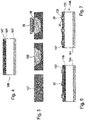
- a crystalline silicon solar cell 10 refer to the z. B. consists of a p-type substrate 12 with pn junction and a front side metallization 14 as a front contact and a backside contact 16 which is formed in particular as a full-surface sintered aluminum layer with a porosity between 5% and 20%, to over the entire back Form back-surface field.
- the rear side that is to say the rear side contact 16 and the front side, that is to say the front side contact 14 must be electrically conductively connected to so-called cells 18, 20 which interconnect adjoining cells.
- the front side extending cell connector 18 of the solar cell 10 extends to the back z. B. a subsequent solar cell and vice versa, the back side cell connector 20 to the front of an upstream solar cell and vice versa.
- the cell connectors 18, 20 can be connected to the front side contact 14 as well as to the back contact 16 to the required extent and with the required strength, it is provided according to the invention that in the contact regions 22, 24 to be produced, the front side contact 14 and / or the back contact 16 is treated. This can be done in particular on the front side by applying strip-shaped solder strips on the front side in the regions in which the cell connectors 18, 20 are to be contacted. On the solder strips then electrically conductive adhesive strips 26 are applied, with which then cell connectors 18 are connected by gluing.
- the cell connectors 18 extend transversely to contact fingers 28, which are shown in dashed lines, as they are continuous from edge to edge. In the exemplary embodiment, a total of three cell connectors 18 extend over the contact fingers 28.
- the function of the contact layer to the cell connectors 18, that is, the busbars takes on the adhesive strip 26 or the previously applied solder material. An additional busbar, as required by the state of the art and basically made of silver, is therefore eliminated.
- the rear side layer 16 which consists in particular of aluminum, is compacted. This can be achieved by pure mechanical treatment z. B. by means of a brush, whereby the porous surface is smoothed and thus a sufficient adhesive surface for the adhesive strip 30 is formed.
- a compaction can z. B. done by laser irradiation, as the DE-A-10 2009 044 038 teaches. In that regard, reference is expressly made to the relevant disclosures.
- Fig. 4 is a further schematic representation of a crystalline silicon solar cell 100 is shown with pn junction 104.
- the silicon solar cell 100 is printed over its entire surface with a paste made of aluminum.
- the aluminum layer 107 which may have a thickness between 30 microns and 50 microns, sintered.
- a eutectic compound Al-Si is formed, which in the Fig. 4 indicated at 106.
- the thickness amounts to approx. 5 ⁇ m.
- the remaining area of the aluminum layer 107 thus has a thickness between 25 ⁇ m and 45 ⁇ m, depending on how the original thickness of the aluminum layer 107 was designed.
- the remaining layer consists of a loosely sintered composite of aluminum spheres and glass frit parts whose strength is not particularly high. If a connector is fastened to the layer 107, only limited withdrawal forces are achieved, in particular ⁇ 1 N, since the pull-off force is determined by the strength of the substrate.
- the layer 107 is solidified by a Ultraschallbelotung means of a solder, so treated. This happens because the solder penetrates into the pores of the loosely sintered aluminum layer 107 and a region 120 (FIG. Fig. 5 ) is formed, which is compressed compared to the layer 107 outside the Beloteten area and thus has a higher strength.
- a region 120 (FIG. Fig. 5 ) is formed, which is compressed compared to the layer 107 outside the Beloteten area and thus has a higher strength.
- the penetration depth of the solder material is between 10 .mu.m to 30 .mu.m.
- the penetration depth depends on the given porosity and consistency of the aluminum paste. With increasing Belotungstemperatur increases the penetration depth of the solder.
- the adhesive is applied in the form of the adhesive strip 30, in order to then hang on the connector 20 in the manner described above and electrically conductively connected to the region 120 and thus the back contact 107 of the solar cell 100 via the adhesive strip 30.
- the solar cell 100 with the densified areas 120 and the connectors 20 is shown in principle. It can be seen that the solder material runs at a distance from the eutectic 106. Of course, according to the previous explanations there is also the possibility that the compacted region 120 extends to the eutectic 106.
- a liquid adhesive instead of solder, it is possible to infiltrate a liquid adhesive to treat the area that is to be electrically connected to a cell connector. This can be done at different temperatures depending on the type of adhesive. For example, it is possible to infiltrate a liquid adhesive at room temperature or 20 ° C. to about 80 ° C., which cures by evaporation of solvent. Other adhesives (eg thermoplastics) only become liquid at higher temperatures. If a corresponding adhesive is infiltrated into the porous aluminum layer 107 of a solar cell 140, stabilization of the strength of the corresponding region 122 of the aluminum layer 107 is achieved in the infiltrated region after curing.
- Curing takes place, for example, by evaporation of the solvent, cooling in the case of thermoplastics, crosslinking in the case of multicomponent adhesives, UV curing in the case of UV-curing adhesives.
- the adhesive together with the porous metal layer 107 forms a solid composite, on which higher withdrawal forces than outside the composite are achieved.
- An adhesive such as adhesive tape 30 and then a connector 20 is then applied to the corresponding regions 122 in the manner described above (FIG. Fig. 7 ).
- the solar cell 140 has a basic structure as the solar cell 100, with the restriction that it is passivated on the back by a SiN or an Al 2 O 3 layer 126.
- the corresponding layer 126 is coated with the screen-printed and sintered aluminum back contact 107 in the manner previously described. Consequently, the majority of the back contact consists only of the composite of aluminum balls and glass frit parts with low strength. In order to achieve regions of higher strength, the previously described infiltration takes place with an adhesive. Alternatively, a Beloten could be performed. Thus, regions 122 are formed which have higher strength compared to the remaining aluminum layer 107.
- the metallic surface is smoothed by mechanical brushing of the surface of the back contact, in which the surface-lying Al spheres, which are very ductile, are flattened by the mechanical deformation and connected to one another. This leads to an improvement of the contact resistance to be applied to the electrically conductive adhesive strip 30 and the applied cell or series connector 20th
- the layer must have a plurality of openings, so that the electrically conductive contact between the aluminum layer 107 and the substrate 12 of the solar cell 10, 100, 140 is made.
Landscapes
- Photovoltaic Devices (AREA)
- Life Sciences & Earth Sciences (AREA)
- Engineering & Computer Science (AREA)
- Sustainable Development (AREA)
- Sustainable Energy (AREA)
Claims (14)
- Procédé de fabrication d'un contact électroconducteur au verso et/ou recto (14, 16) d'une photopile (10, 100, 140), le contact étant relié à un connecteur (18, 20) interconnectant des photopiles au moyen d'un adhésif (30, 26),
caractérisé en ce
que la surface du recto et/ou verso (14, 16) de la photopile (10, 100, 140) est traitée dans la zone de contact à former par au moins une mesure du groupe compactage au moins partiel, l'application de matériau de soudure se faisant par ultrasons, et que, après le traitement dans cette zone, un adhésif pâteux en forme de bande ou une bande adhésive (30, 26) est appliqué(e)dans la zone en tant qu'adhésif, tout en permettant simultanément une connexion électroconductrice. - Procédé selon la revendication 1,
caractérisé en ce
que le matériau utilisé pour l'adhésif est sur la base d'au moins un matériau du groupe résine époxy, résine phénolique, résine phénoxy, polyuréthane, silicone, un acrylate durcissable aux UV, étant en particulier électroconducteur. - Procédé selon au moins la revendication 1,
caractérisé en ce
que le compactage au moins partiel de la surface ou d'une zone près de la surface se fait par application par ultrasons, irradiation laser, traitement thermique et/ou traitement de surface mécanique. - Procédé selon la revendication 3,
caractérisé en ce
que le traitement de surface mécanique se fait à l'aide d'une brosse. - Procédé selon au moins l'une des précédentes revendications,
caractérisé en ce
qu'un matériau soudable ou mouillable par métal est incorporé par alliage dans la surface du verso (16) de la photopile, en particulier au moins un matériau du groupe Sn, Pb, In, Ga, Cd, Fe, Ag, Au, Ti, Hf, Zn, Mg, Ca, Ba, un matériau de brasage ou un mélange de matériaux du groupe. - Procédé selon au moins l'une des précédentes revendications,
caractérisé en ce
que la photopile utilisée est une photopile (10, 100, 140) présentant sur toute la surface du verso une couche poreuse (102) comme contact arrière, dans laquelle des zones en forme de blocs ou de bandes sont conçues en tant que zones auxquelles l'adhésif est relié. - Procédé selon au moins l'une des précédentes revendications,
caractérisé en ce
que la photopile utilisée est une photopile (10, 100, 140) avec un recto sans barre omnibus avec des collecteurs de courant (doigts) (28) s'étendant approximativement parallèlement les uns aux autres et auxquels est relié(e) l'adhésif apposé en forme de bandes ou la bande adhésive (30, 26), lequel ou laquelle s'étend transversalement aux collecteurs de courant. - Procédé selon au moins l'une des précédentes revendications,
caractérisé en ce
que la photopile (10, 100, 140) utilisée est une photopile cristalline, en particulier une photopile cristalline au silicium, ou une photopile en couches minces. - Procédé selon au moins l'une des précédentes revendications,
caractérisé en ce
qu'un connecteur électroconducteur, constitué en particulier de cuivre brasé, de cuivre galvanisé ou d'aluminium ou d'aluminium brasé, est raccordé à l'adhésif (30, 26). - Procédé selon au moins l'une des précédentes revendications,
caractérisé en ce
que l'adhésif est apposé sur la zone avec une largeur B de 0,5 mm ≤ B <10 mm, en particulier 0,8 mm ≤ B ≤2 mm, et/ou une épaisseur D avec 3 µm ≤ D ≤50 µm. - Procédé selon au moins l'une des précédentes revendications,
caractérisé en ce
que la zone devant être revêtue d'adhésif doit être préalablement revêtue d'un silane fonctionnel du groupe éthoxy- ou méthoxysilane avec un autre groupe fonctionnel amino ou époxy. - Procédé selon au moins l'une des précédentes revendications,
caractérisé en ce
que l'adhésif utilisé est un adhésif (30, 26) contenant en tant que charge au moins un matériau du groupe argent, cuivre, nickel, aluminium, or, graphite, zinc, étain, palladium, - Procédé selon au moins l'une des précédentes revendications,
caractérisé en ce
que la zone de la surface dans laquelle le connecteur (18, 20) est relié à la photopile (10, 100, 140) est lissée au moyen d'un matériau adhésif, que l'adhésif est ensuite apposé sur le matériau adhésif et que finalement le connecteur (18, 20) est raccordé à l'adhésif en étant électroconduteur. - Procédé selon au moins l'une des précédentes revendications,
caractérisé en ce
que le matériau de brasage est tout d'abord introduit dans la zone de la surface dans laquelle le connecteur (18, 20) est en contact, puis l'adhésif est apposé sur la zone et que cette dernière est finalement reliée au collecteur.
Applications Claiming Priority (2)
| Application Number | Priority Date | Filing Date | Title |
|---|---|---|---|
| DE102012100535A DE102012100535A1 (de) | 2012-01-23 | 2012-01-23 | Verfahren zum Herstellen eines elektrisch leitenden Kontakts auf einer Solarzelle |
| PCT/EP2013/051143 WO2013110607A1 (fr) | 2012-01-23 | 2013-01-22 | Procédé de fabrication d'un contact électroconducteur sur une photopile |
Publications (2)
| Publication Number | Publication Date |
|---|---|
| EP2807676A1 EP2807676A1 (fr) | 2014-12-03 |
| EP2807676B1 true EP2807676B1 (fr) | 2019-10-16 |
Family
ID=47624052
Family Applications (1)
| Application Number | Title | Priority Date | Filing Date |
|---|---|---|---|
| EP13701609.3A Active EP2807676B1 (fr) | 2012-01-23 | 2013-01-22 | Procédé de fabrication d'un contact électroconducteur sur une photopile |
Country Status (5)
| Country | Link |
|---|---|
| US (1) | US9666751B2 (fr) |
| EP (1) | EP2807676B1 (fr) |
| CN (1) | CN104247034A (fr) |
| DE (1) | DE102012100535A1 (fr) |
| WO (1) | WO2013110607A1 (fr) |
Families Citing this family (9)
| Publication number | Priority date | Publication date | Assignee | Title |
|---|---|---|---|---|
| DE102013204828A1 (de) * | 2013-03-19 | 2014-09-25 | Fraunhofer-Gesellschaft zur Förderung der angewandten Forschung e.V. | Rückseitenkontaktiertes Halbleiterbauelement und Verfahren zu dessen Herstellung |
| TW201445757A (zh) * | 2013-03-22 | 2014-12-01 | 3M Innovative Properties Co | 包含導電膠帶之模組及太陽能電池及彼等之製造與使用方法 |
| US10186628B2 (en) | 2014-06-20 | 2019-01-22 | Vismunda Srl | Apparatus for the automatic horizontal assembly of photovoltaic panels |
| US9888584B2 (en) | 2014-12-31 | 2018-02-06 | Invensas Corporation | Contact structures with porous networks for solder connections, and methods of fabricating same |
| ES2772256T3 (es) * | 2015-11-06 | 2020-07-07 | Meyer Burger Switzerland Ag | Láminas conductoras de polímero, celdas solares y métodos para producirlos |
| WO2018159306A1 (fr) * | 2017-02-28 | 2018-09-07 | アートビーム有限会社 | Cellule solaire et son procédé de production |
| JP6932659B2 (ja) * | 2017-03-15 | 2021-09-08 | アートビーム有限会社 | 太陽電池および太陽電池の製造方法 |
| CN110383500A (zh) * | 2017-02-28 | 2019-10-25 | 亚特比目有限会社 | 太阳能电池及太阳能电池的制造方法 |
| CN109524487B (zh) * | 2018-11-26 | 2020-11-10 | 西安交通大学 | 具有微观圆滑棱角的绒面电池硅其及制备方法 |
Citations (1)
| Publication number | Priority date | Publication date | Assignee | Title |
|---|---|---|---|---|
| JPH10313126A (ja) * | 1997-05-13 | 1998-11-24 | Sharp Corp | 太陽電池素子及びその電極の表面処理方法及び太陽電池モジュール |
Family Cites Families (18)
| Publication number | Priority date | Publication date | Assignee | Title |
|---|---|---|---|---|
| JPH03183527A (ja) | 1989-12-13 | 1991-08-09 | Hitachi Constr Mach Co Ltd | 超音波接合装置 |
| JPH03188180A (ja) | 1989-12-18 | 1991-08-16 | Hitachi Chem Co Ltd | 導電性フイルム状接着剤,接着法,半導体装置および半導体装置の製造法 |
| JPH0645024A (ja) | 1992-07-22 | 1994-02-18 | Hitachi Chem Co Ltd | 異方導電性接着フィルム |
| US7264991B1 (en) * | 2000-10-13 | 2007-09-04 | Bridge Semiconductor Corporation | Method of connecting a conductive trace to a semiconductor chip using conductive adhesive |
| TWI487124B (zh) * | 2006-08-25 | 2015-06-01 | Sanyo Electric Co | 太陽電池模組及太陽電池模組的製造方法 |
| CN100541821C (zh) * | 2006-09-13 | 2009-09-16 | 日立电线株式会社 | 太阳能电池用连接引线和它的制造方法及太阳能电池 |
| JP2008098607A (ja) * | 2006-09-13 | 2008-04-24 | Hitachi Cable Ltd | 太陽電池用接続リード線及びその製造方法並びに太陽電池 |
| EP2146355A1 (fr) * | 2007-05-09 | 2010-01-20 | Hitachi Chemical Company, Ltd. | Élément de liaison conducteur, structure de liaison et module de cellule solaire |
| TWI449183B (zh) | 2007-06-13 | 2014-08-11 | Schott Solar Ag | 半導體元件及製造金屬半導體接點之方法 |
| DE102008019769A1 (de) * | 2008-04-18 | 2009-10-22 | Henkel Ag & Co. Kgaa | Verfahren zum Verkleben eines ersten Bauteils mit einem zweiten Bauteil |
| JP6085076B2 (ja) * | 2009-03-16 | 2017-02-22 | リンテック株式会社 | 粘着シートおよび半導体ウエハの加工方法、半導体チップの製造方法 |
| JP5375450B2 (ja) * | 2009-08-31 | 2013-12-25 | 三洋電機株式会社 | 太陽電池セル及び太陽電池モジュール |
| DE102009044038A1 (de) | 2009-09-17 | 2011-03-31 | Schott Solar Ag | Verfahren zur Herstellung eines Kontaktbereichs eines elektronischen Bauteils |
| JP2011108969A (ja) * | 2009-11-20 | 2011-06-02 | Hitachi Cable Ltd | 太陽電池モジュールの製造方法、及び太陽電池用配線基板 |
| DE102010000520A1 (de) | 2010-02-23 | 2011-08-25 | SCHOTT Solar AG, 55122 | Verfahren und Vorrichtung zum Aufbringen von Lot auf ein Werkstück |
| DE102010016814B3 (de) | 2010-05-05 | 2011-10-06 | Schott Solar Ag | Verfahren und Vorrichtung zum Aufbringen von Lot auf ein Werkstück |
| WO2012135052A1 (fr) * | 2011-03-25 | 2012-10-04 | Kevin Michael Coakley | Interconnexion à feuilles pour cellules solaires à contact arrière |
| WO2012138986A1 (fr) * | 2011-04-07 | 2012-10-11 | Specialized Technology Resources, Inc | Matériau d'encapsulation pour modules photovoltaïques terrestres |
-
2012
- 2012-01-23 DE DE102012100535A patent/DE102012100535A1/de not_active Ceased
-
2013
- 2013-01-22 US US14/373,951 patent/US9666751B2/en not_active Expired - Fee Related
- 2013-01-22 WO PCT/EP2013/051143 patent/WO2013110607A1/fr not_active Ceased
- 2013-01-22 CN CN201380006350.2A patent/CN104247034A/zh active Pending
- 2013-01-22 EP EP13701609.3A patent/EP2807676B1/fr active Active
Patent Citations (1)
| Publication number | Priority date | Publication date | Assignee | Title |
|---|---|---|---|---|
| JPH10313126A (ja) * | 1997-05-13 | 1998-11-24 | Sharp Corp | 太陽電池素子及びその電極の表面処理方法及び太陽電池モジュール |
Also Published As
| Publication number | Publication date |
|---|---|
| CN104247034A (zh) | 2014-12-24 |
| US9666751B2 (en) | 2017-05-30 |
| EP2807676A1 (fr) | 2014-12-03 |
| DE102012100535A1 (de) | 2013-07-25 |
| US20150050773A1 (en) | 2015-02-19 |
| WO2013110607A1 (fr) | 2013-08-01 |
Similar Documents
| Publication | Publication Date | Title |
|---|---|---|
| EP2807676B1 (fr) | Procédé de fabrication d'un contact électroconducteur sur une photopile | |
| DE69618458T2 (de) | Halbleiterteil mit einem zu einem verdrahtungsträger elektrisch verbundenem chip | |
| EP0275433B1 (fr) | Procédé pour fixer des composants électroniques sur un substrat, feuille pour réaliser le procédé et procédé pour la fabrication de la feuille | |
| EP2003699B1 (fr) | Composant semi-conducteur et procédé de fabrication d'un contact entre un semi-conducteur et un métal | |
| DE10232991A1 (de) | Dreischichtiger anisotroper leitender Klebstofffilm mit hohem Haftvermögen | |
| DE112012004671T5 (de) | Solarzellenmodul und Herstellungsverfahren für dieses | |
| EP2390904A2 (fr) | Procédé d'interconnexion de pression à basse température de deux partenaires de liaison et agencement ainsi fabriqué | |
| WO2012171968A1 (fr) | Procédé de raccordement électrique de plusieurs cellules solaires et module photovoltaïque associé | |
| WO2001065603A1 (fr) | Assemblage colle thermoconducteur, et procede de realisation d'un assemblage colle thermoconducteur | |
| DE112011104782T5 (de) | Photovoltaikmodul und Verfahren | |
| EP2553038B1 (fr) | Agencement thermoconducteur entre deux éléments et procédé de fabrication d'un agencement thermoconducteur | |
| EP3392916A1 (fr) | Composé d'aluminium résistant au vieillissement pour cellules solaires | |
| DE102009053416B4 (de) | Verfahren zur Herstellung und Verschaltung von Solarzellenanordnungen und Solarzellenanordnung | |
| WO2013067998A1 (fr) | Cellule solaire à plaque de semi-conducteur, mise en contact des deux côtés, sa face arrière ayant subi une passivation de surface | |
| DE102008044354B4 (de) | Solarzellensystem, Solarzellenmodul und Verfahren zur Herstellung eines Solarzellensystems | |
| DE202019004359U1 (de) | Flachleiteranschlusselement | |
| DE102015107712B3 (de) | Verfahren zur Herstellung eines Schaltungsträgers | |
| EP2737542B1 (fr) | Procédé de fabrication d'une cellule solaire | |
| WO2024051894A1 (fr) | Procédé de production d'un produit de module solaire semi-fini | |
| DE102015007157A1 (de) | Flächige elektrische Kontaktierung und Verfahren zu deren Herstellung | |
| DE102018214778A1 (de) | Verfahren zur Fertigung von Leiterbahnen und Elektronikmodul | |
| DE102011083423A1 (de) | Kontaktfederanordnung und Verfahren zur Herstellung derselben | |
| DE102010041917B4 (de) | Schaltungsanordnung und Verfahren zu deren Herstellung | |
| DE102010024331B4 (de) | Verfahren zur Verklebung eines bandförmigen Leiters mit einer Solarzelle, Anordnung mit der Verklebung und Verwendung eines Piezo-Jet-Dispensers dafür | |
| DE102025101452A1 (de) | Halbleitervorrichtung, verfahren zur herstellung einer halbleitervorrichtung und substrat |
Legal Events
| Date | Code | Title | Description |
|---|---|---|---|
| PUAI | Public reference made under article 153(3) epc to a published international application that has entered the european phase |
Free format text: ORIGINAL CODE: 0009012 |
|
| 17P | Request for examination filed |
Effective date: 20140818 |
|
| AK | Designated contracting states |
Kind code of ref document: A1 Designated state(s): AL AT BE BG CH CY CZ DE DK EE ES FI FR GB GR HR HU IE IS IT LI LT LU LV MC MK MT NL NO PL PT RO RS SE SI SK SM TR |
|
| DAX | Request for extension of the european patent (deleted) | ||
| STAA | Information on the status of an ep patent application or granted ep patent |
Free format text: STATUS: EXAMINATION IS IN PROGRESS |
|
| 17Q | First examination report despatched |
Effective date: 20170222 |
|
| GRAP | Despatch of communication of intention to grant a patent |
Free format text: ORIGINAL CODE: EPIDOSNIGR1 |
|
| STAA | Information on the status of an ep patent application or granted ep patent |
Free format text: STATUS: GRANT OF PATENT IS INTENDED |
|
| INTG | Intention to grant announced |
Effective date: 20190108 |
|
| RAP1 | Party data changed (applicant data changed or rights of an application transferred) |
Owner name: FRAUNHOFER-GESELLSCHAFT ZUR FOERDERUNG DER ANGEWAN |
|
| GRAS | Grant fee paid |
Free format text: ORIGINAL CODE: EPIDOSNIGR3 |
|
| GRAJ | Information related to disapproval of communication of intention to grant by the applicant or resumption of examination proceedings by the epo deleted |
Free format text: ORIGINAL CODE: EPIDOSDIGR1 |
|
| GRAL | Information related to payment of fee for publishing/printing deleted |
Free format text: ORIGINAL CODE: EPIDOSDIGR3 |
|
| STAA | Information on the status of an ep patent application or granted ep patent |
Free format text: STATUS: EXAMINATION IS IN PROGRESS |
|
| GRAP | Despatch of communication of intention to grant a patent |
Free format text: ORIGINAL CODE: EPIDOSNIGR1 |
|
| STAA | Information on the status of an ep patent application or granted ep patent |
Free format text: STATUS: GRANT OF PATENT IS INTENDED |
|
| INTC | Intention to grant announced (deleted) | ||
| RIN1 | Information on inventor provided before grant (corrected) |
Inventor name: VON CAMPE, HILMER Inventor name: MARTINI, MARCEL Inventor name: MEYER, STEFAN Inventor name: BOEHME, SVEN Inventor name: HUBER, STEPHAN |
|
| INTG | Intention to grant announced |
Effective date: 20190604 |
|
| GRAA | (expected) grant |
Free format text: ORIGINAL CODE: 0009210 |
|
| STAA | Information on the status of an ep patent application or granted ep patent |
Free format text: STATUS: THE PATENT HAS BEEN GRANTED |
|
| AK | Designated contracting states |
Kind code of ref document: B1 Designated state(s): AL AT BE BG CH CY CZ DE DK EE ES FI FR GB GR HR HU IE IS IT LI LT LU LV MC MK MT NL NO PL PT RO RS SE SI SK SM TR |
|
| REG | Reference to a national code |
Ref country code: GB Ref legal event code: FG4D Free format text: NOT ENGLISH |
|
| REG | Reference to a national code |
Ref country code: CH Ref legal event code: EP |
|
| REG | Reference to a national code |
Ref country code: DE Ref legal event code: R096 Ref document number: 502013013759 Country of ref document: DE |
|
| REG | Reference to a national code |
Ref country code: IE Ref legal event code: FG4D Free format text: LANGUAGE OF EP DOCUMENT: GERMAN |
|
| REG | Reference to a national code |
Ref country code: AT Ref legal event code: REF Ref document number: 1192138 Country of ref document: AT Kind code of ref document: T Effective date: 20191115 |
|
| REG | Reference to a national code |
Ref country code: NL Ref legal event code: MP Effective date: 20191016 |
|
| REG | Reference to a national code |
Ref country code: LT Ref legal event code: MG4D |
|
| PG25 | Lapsed in a contracting state [announced via postgrant information from national office to epo] |
Ref country code: PL Free format text: LAPSE BECAUSE OF FAILURE TO SUBMIT A TRANSLATION OF THE DESCRIPTION OR TO PAY THE FEE WITHIN THE PRESCRIBED TIME-LIMIT Effective date: 20191016 Ref country code: LT Free format text: LAPSE BECAUSE OF FAILURE TO SUBMIT A TRANSLATION OF THE DESCRIPTION OR TO PAY THE FEE WITHIN THE PRESCRIBED TIME-LIMIT Effective date: 20191016 Ref country code: GR Free format text: LAPSE BECAUSE OF FAILURE TO SUBMIT A TRANSLATION OF THE DESCRIPTION OR TO PAY THE FEE WITHIN THE PRESCRIBED TIME-LIMIT Effective date: 20200117 Ref country code: NO Free format text: LAPSE BECAUSE OF FAILURE TO SUBMIT A TRANSLATION OF THE DESCRIPTION OR TO PAY THE FEE WITHIN THE PRESCRIBED TIME-LIMIT Effective date: 20200116 Ref country code: NL Free format text: LAPSE BECAUSE OF FAILURE TO SUBMIT A TRANSLATION OF THE DESCRIPTION OR TO PAY THE FEE WITHIN THE PRESCRIBED TIME-LIMIT Effective date: 20191016 Ref country code: ES Free format text: LAPSE BECAUSE OF FAILURE TO SUBMIT A TRANSLATION OF THE DESCRIPTION OR TO PAY THE FEE WITHIN THE PRESCRIBED TIME-LIMIT Effective date: 20191016 Ref country code: PT Free format text: LAPSE BECAUSE OF FAILURE TO SUBMIT A TRANSLATION OF THE DESCRIPTION OR TO PAY THE FEE WITHIN THE PRESCRIBED TIME-LIMIT Effective date: 20200217 Ref country code: SE Free format text: LAPSE BECAUSE OF FAILURE TO SUBMIT A TRANSLATION OF THE DESCRIPTION OR TO PAY THE FEE WITHIN THE PRESCRIBED TIME-LIMIT Effective date: 20191016 Ref country code: LV Free format text: LAPSE BECAUSE OF FAILURE TO SUBMIT A TRANSLATION OF THE DESCRIPTION OR TO PAY THE FEE WITHIN THE PRESCRIBED TIME-LIMIT Effective date: 20191016 Ref country code: BG Free format text: LAPSE BECAUSE OF FAILURE TO SUBMIT A TRANSLATION OF THE DESCRIPTION OR TO PAY THE FEE WITHIN THE PRESCRIBED TIME-LIMIT Effective date: 20200116 Ref country code: FI Free format text: LAPSE BECAUSE OF FAILURE TO SUBMIT A TRANSLATION OF THE DESCRIPTION OR TO PAY THE FEE WITHIN THE PRESCRIBED TIME-LIMIT Effective date: 20191016 |
|
| PG25 | Lapsed in a contracting state [announced via postgrant information from national office to epo] |
Ref country code: IS Free format text: LAPSE BECAUSE OF FAILURE TO SUBMIT A TRANSLATION OF THE DESCRIPTION OR TO PAY THE FEE WITHIN THE PRESCRIBED TIME-LIMIT Effective date: 20200224 Ref country code: RS Free format text: LAPSE BECAUSE OF FAILURE TO SUBMIT A TRANSLATION OF THE DESCRIPTION OR TO PAY THE FEE WITHIN THE PRESCRIBED TIME-LIMIT Effective date: 20191016 Ref country code: HR Free format text: LAPSE BECAUSE OF FAILURE TO SUBMIT A TRANSLATION OF THE DESCRIPTION OR TO PAY THE FEE WITHIN THE PRESCRIBED TIME-LIMIT Effective date: 20191016 |
|
| PG25 | Lapsed in a contracting state [announced via postgrant information from national office to epo] |
Ref country code: AL Free format text: LAPSE BECAUSE OF FAILURE TO SUBMIT A TRANSLATION OF THE DESCRIPTION OR TO PAY THE FEE WITHIN THE PRESCRIBED TIME-LIMIT Effective date: 20191016 |
|
| REG | Reference to a national code |
Ref country code: DE Ref legal event code: R097 Ref document number: 502013013759 Country of ref document: DE |
|
| PG2D | Information on lapse in contracting state deleted |
Ref country code: IS |
|
| PG25 | Lapsed in a contracting state [announced via postgrant information from national office to epo] |
Ref country code: EE Free format text: LAPSE BECAUSE OF FAILURE TO SUBMIT A TRANSLATION OF THE DESCRIPTION OR TO PAY THE FEE WITHIN THE PRESCRIBED TIME-LIMIT Effective date: 20191016 Ref country code: DK Free format text: LAPSE BECAUSE OF FAILURE TO SUBMIT A TRANSLATION OF THE DESCRIPTION OR TO PAY THE FEE WITHIN THE PRESCRIBED TIME-LIMIT Effective date: 20191016 Ref country code: RO Free format text: LAPSE BECAUSE OF FAILURE TO SUBMIT A TRANSLATION OF THE DESCRIPTION OR TO PAY THE FEE WITHIN THE PRESCRIBED TIME-LIMIT Effective date: 20191016 Ref country code: CZ Free format text: LAPSE BECAUSE OF FAILURE TO SUBMIT A TRANSLATION OF THE DESCRIPTION OR TO PAY THE FEE WITHIN THE PRESCRIBED TIME-LIMIT Effective date: 20191016 Ref country code: IS Free format text: LAPSE BECAUSE OF FAILURE TO SUBMIT A TRANSLATION OF THE DESCRIPTION OR TO PAY THE FEE WITHIN THE PRESCRIBED TIME-LIMIT Effective date: 20200216 |
|
| PLBE | No opposition filed within time limit |
Free format text: ORIGINAL CODE: 0009261 |
|
| STAA | Information on the status of an ep patent application or granted ep patent |
Free format text: STATUS: NO OPPOSITION FILED WITHIN TIME LIMIT |
|
| PG25 | Lapsed in a contracting state [announced via postgrant information from national office to epo] |
Ref country code: IT Free format text: LAPSE BECAUSE OF FAILURE TO SUBMIT A TRANSLATION OF THE DESCRIPTION OR TO PAY THE FEE WITHIN THE PRESCRIBED TIME-LIMIT Effective date: 20191016 Ref country code: MC Free format text: LAPSE BECAUSE OF FAILURE TO SUBMIT A TRANSLATION OF THE DESCRIPTION OR TO PAY THE FEE WITHIN THE PRESCRIBED TIME-LIMIT Effective date: 20191016 Ref country code: SK Free format text: LAPSE BECAUSE OF FAILURE TO SUBMIT A TRANSLATION OF THE DESCRIPTION OR TO PAY THE FEE WITHIN THE PRESCRIBED TIME-LIMIT Effective date: 20191016 Ref country code: SM Free format text: LAPSE BECAUSE OF FAILURE TO SUBMIT A TRANSLATION OF THE DESCRIPTION OR TO PAY THE FEE WITHIN THE PRESCRIBED TIME-LIMIT Effective date: 20191016 |
|
| REG | Reference to a national code |
Ref country code: CH Ref legal event code: PL |
|
| 26N | No opposition filed |
Effective date: 20200717 |
|
| GBPC | Gb: european patent ceased through non-payment of renewal fee |
Effective date: 20200122 |
|
| REG | Reference to a national code |
Ref country code: BE Ref legal event code: MM Effective date: 20200131 |
|
| PG25 | Lapsed in a contracting state [announced via postgrant information from national office to epo] |
Ref country code: LU Free format text: LAPSE BECAUSE OF NON-PAYMENT OF DUE FEES Effective date: 20200122 Ref country code: GB Free format text: LAPSE BECAUSE OF NON-PAYMENT OF DUE FEES Effective date: 20200122 |
|
| PG25 | Lapsed in a contracting state [announced via postgrant information from national office to epo] |
Ref country code: LI Free format text: LAPSE BECAUSE OF NON-PAYMENT OF DUE FEES Effective date: 20200131 Ref country code: CH Free format text: LAPSE BECAUSE OF NON-PAYMENT OF DUE FEES Effective date: 20200131 Ref country code: SI Free format text: LAPSE BECAUSE OF FAILURE TO SUBMIT A TRANSLATION OF THE DESCRIPTION OR TO PAY THE FEE WITHIN THE PRESCRIBED TIME-LIMIT Effective date: 20191016 Ref country code: BE Free format text: LAPSE BECAUSE OF NON-PAYMENT OF DUE FEES Effective date: 20200131 |
|
| PG25 | Lapsed in a contracting state [announced via postgrant information from national office to epo] |
Ref country code: IE Free format text: LAPSE BECAUSE OF NON-PAYMENT OF DUE FEES Effective date: 20200122 |
|
| REG | Reference to a national code |
Ref country code: AT Ref legal event code: MM01 Ref document number: 1192138 Country of ref document: AT Kind code of ref document: T Effective date: 20200122 |
|
| PGFP | Annual fee paid to national office [announced via postgrant information from national office to epo] |
Ref country code: FR Payment date: 20210120 Year of fee payment: 9 |
|
| PG25 | Lapsed in a contracting state [announced via postgrant information from national office to epo] |
Ref country code: AT Free format text: LAPSE BECAUSE OF NON-PAYMENT OF DUE FEES Effective date: 20200122 |
|
| PGFP | Annual fee paid to national office [announced via postgrant information from national office to epo] |
Ref country code: DE Payment date: 20210120 Year of fee payment: 9 |
|
| PG25 | Lapsed in a contracting state [announced via postgrant information from national office to epo] |
Ref country code: TR Free format text: LAPSE BECAUSE OF FAILURE TO SUBMIT A TRANSLATION OF THE DESCRIPTION OR TO PAY THE FEE WITHIN THE PRESCRIBED TIME-LIMIT Effective date: 20191016 Ref country code: MT Free format text: LAPSE BECAUSE OF FAILURE TO SUBMIT A TRANSLATION OF THE DESCRIPTION OR TO PAY THE FEE WITHIN THE PRESCRIBED TIME-LIMIT Effective date: 20191016 Ref country code: CY Free format text: LAPSE BECAUSE OF FAILURE TO SUBMIT A TRANSLATION OF THE DESCRIPTION OR TO PAY THE FEE WITHIN THE PRESCRIBED TIME-LIMIT Effective date: 20191016 |
|
| PG25 | Lapsed in a contracting state [announced via postgrant information from national office to epo] |
Ref country code: MK Free format text: LAPSE BECAUSE OF FAILURE TO SUBMIT A TRANSLATION OF THE DESCRIPTION OR TO PAY THE FEE WITHIN THE PRESCRIBED TIME-LIMIT Effective date: 20191016 |
|
| REG | Reference to a national code |
Ref country code: DE Ref legal event code: R119 Ref document number: 502013013759 Country of ref document: DE |
|
| PG25 | Lapsed in a contracting state [announced via postgrant information from national office to epo] |
Ref country code: DE Free format text: LAPSE BECAUSE OF NON-PAYMENT OF DUE FEES Effective date: 20220802 |
|
| PG25 | Lapsed in a contracting state [announced via postgrant information from national office to epo] |
Ref country code: FR Free format text: LAPSE BECAUSE OF NON-PAYMENT OF DUE FEES Effective date: 20220131 |