EP2808150B1 - Surface treatment method of an electronic device case - Google Patents
Surface treatment method of an electronic device case Download PDFInfo
- Publication number
- EP2808150B1 EP2808150B1 EP14169745.8A EP14169745A EP2808150B1 EP 2808150 B1 EP2808150 B1 EP 2808150B1 EP 14169745 A EP14169745 A EP 14169745A EP 2808150 B1 EP2808150 B1 EP 2808150B1
- Authority
- EP
- European Patent Office
- Prior art keywords
- sheet material
- raw sheet
- pattern
- mold
- molding liquid
- Prior art date
- Legal status (The legal status is an assumption and is not a legal conclusion. Google has not performed a legal analysis and makes no representation as to the accuracy of the status listed.)
- Active
Links
Images




Classifications
-
- B—PERFORMING OPERATIONS; TRANSPORTING
- B29—WORKING OF PLASTICS; WORKING OF SUBSTANCES IN A PLASTIC STATE IN GENERAL
- B29C—SHAPING OR JOINING OF PLASTICS; SHAPING OF MATERIAL IN A PLASTIC STATE, NOT OTHERWISE PROVIDED FOR; AFTER-TREATMENT OF THE SHAPED PRODUCTS, e.g. REPAIRING
- B29C43/00—Compression moulding, i.e. applying external pressure to flow the moulding material; Apparatus therefor
- B29C43/02—Compression moulding, i.e. applying external pressure to flow the moulding material; Apparatus therefor of articles of definite length, i.e. discrete articles
- B29C43/20—Making multilayered or multicoloured articles
-
- G—PHYSICS
- G03—PHOTOGRAPHY; CINEMATOGRAPHY; ANALOGOUS TECHNIQUES USING WAVES OTHER THAN OPTICAL WAVES; ELECTROGRAPHY; HOLOGRAPHY
- G03F—PHOTOMECHANICAL PRODUCTION OF TEXTURED OR PATTERNED SURFACES, e.g. FOR PRINTING, FOR PROCESSING OF SEMICONDUCTOR DEVICES; MATERIALS THEREFOR; ORIGINALS THEREFOR; APPARATUS SPECIALLY ADAPTED THEREFOR
- G03F7/00—Photomechanical, e.g. photolithographic, production of textured or patterned surfaces, e.g. printing surfaces; Materials therefor, e.g. comprising photoresists; Apparatus specially adapted therefor
- G03F7/0002—Lithographic processes using patterning methods other than those involving the exposure to radiation, e.g. by stamping
-
- B—PERFORMING OPERATIONS; TRANSPORTING
- B29—WORKING OF PLASTICS; WORKING OF SUBSTANCES IN A PLASTIC STATE IN GENERAL
- B29C—SHAPING OR JOINING OF PLASTICS; SHAPING OF MATERIAL IN A PLASTIC STATE, NOT OTHERWISE PROVIDED FOR; AFTER-TREATMENT OF THE SHAPED PRODUCTS, e.g. REPAIRING
- B29C35/00—Heating, cooling or curing, e.g. crosslinking or vulcanising; Apparatus therefor
- B29C35/02—Heating or curing, e.g. crosslinking or vulcanizing during moulding, e.g. in a mould
- B29C35/08—Heating or curing, e.g. crosslinking or vulcanizing during moulding, e.g. in a mould by wave energy or particle radiation
-
- B—PERFORMING OPERATIONS; TRANSPORTING
- B29—WORKING OF PLASTICS; WORKING OF SUBSTANCES IN A PLASTIC STATE IN GENERAL
- B29C—SHAPING OR JOINING OF PLASTICS; SHAPING OF MATERIAL IN A PLASTIC STATE, NOT OTHERWISE PROVIDED FOR; AFTER-TREATMENT OF THE SHAPED PRODUCTS, e.g. REPAIRING
- B29C35/00—Heating, cooling or curing, e.g. crosslinking or vulcanising; Apparatus therefor
- B29C35/02—Heating or curing, e.g. crosslinking or vulcanizing during moulding, e.g. in a mould
- B29C35/08—Heating or curing, e.g. crosslinking or vulcanizing during moulding, e.g. in a mould by wave energy or particle radiation
- B29C35/0805—Heating or curing, e.g. crosslinking or vulcanizing during moulding, e.g. in a mould by wave energy or particle radiation using electromagnetic radiation
-
- B—PERFORMING OPERATIONS; TRANSPORTING
- B29—WORKING OF PLASTICS; WORKING OF SUBSTANCES IN A PLASTIC STATE IN GENERAL
- B29C—SHAPING OR JOINING OF PLASTICS; SHAPING OF MATERIAL IN A PLASTIC STATE, NOT OTHERWISE PROVIDED FOR; AFTER-TREATMENT OF THE SHAPED PRODUCTS, e.g. REPAIRING
- B29C37/00—Component parts, details, accessories or auxiliary operations, not covered by group B29C33/00 or B29C35/00
- B29C37/0053—Moulding articles characterised by the shape of the surface, e.g. ribs, high polish
-
- B—PERFORMING OPERATIONS; TRANSPORTING
- B29—WORKING OF PLASTICS; WORKING OF SUBSTANCES IN A PLASTIC STATE IN GENERAL
- B29C—SHAPING OR JOINING OF PLASTICS; SHAPING OF MATERIAL IN A PLASTIC STATE, NOT OTHERWISE PROVIDED FOR; AFTER-TREATMENT OF THE SHAPED PRODUCTS, e.g. REPAIRING
- B29C43/00—Compression moulding, i.e. applying external pressure to flow the moulding material; Apparatus therefor
- B29C43/02—Compression moulding, i.e. applying external pressure to flow the moulding material; Apparatus therefor of articles of definite length, i.e. discrete articles
- B29C43/021—Compression moulding, i.e. applying external pressure to flow the moulding material; Apparatus therefor of articles of definite length, i.e. discrete articles characterised by the shape of the surface
-
- B—PERFORMING OPERATIONS; TRANSPORTING
- B29—WORKING OF PLASTICS; WORKING OF SUBSTANCES IN A PLASTIC STATE IN GENERAL
- B29C—SHAPING OR JOINING OF PLASTICS; SHAPING OF MATERIAL IN A PLASTIC STATE, NOT OTHERWISE PROVIDED FOR; AFTER-TREATMENT OF THE SHAPED PRODUCTS, e.g. REPAIRING
- B29C43/00—Compression moulding, i.e. applying external pressure to flow the moulding material; Apparatus therefor
- B29C43/02—Compression moulding, i.e. applying external pressure to flow the moulding material; Apparatus therefor of articles of definite length, i.e. discrete articles
- B29C43/18—Compression moulding, i.e. applying external pressure to flow the moulding material; Apparatus therefor of articles of definite length, i.e. discrete articles incorporating preformed parts or layers, e.g. compression moulding around inserts or for coating articles
-
- B—PERFORMING OPERATIONS; TRANSPORTING
- B29—WORKING OF PLASTICS; WORKING OF SUBSTANCES IN A PLASTIC STATE IN GENERAL
- B29C—SHAPING OR JOINING OF PLASTICS; SHAPING OF MATERIAL IN A PLASTIC STATE, NOT OTHERWISE PROVIDED FOR; AFTER-TREATMENT OF THE SHAPED PRODUCTS, e.g. REPAIRING
- B29C43/00—Compression moulding, i.e. applying external pressure to flow the moulding material; Apparatus therefor
- B29C43/32—Component parts, details or accessories; Auxiliary operations
- B29C43/36—Moulds for making articles of definite length, i.e. discrete articles
- B29C43/40—Moulds for making articles of definite length, i.e. discrete articles with means for cutting the article
-
- B—PERFORMING OPERATIONS; TRANSPORTING
- B29—WORKING OF PLASTICS; WORKING OF SUBSTANCES IN A PLASTIC STATE IN GENERAL
- B29C—SHAPING OR JOINING OF PLASTICS; SHAPING OF MATERIAL IN A PLASTIC STATE, NOT OTHERWISE PROVIDED FOR; AFTER-TREATMENT OF THE SHAPED PRODUCTS, e.g. REPAIRING
- B29C45/00—Injection moulding, i.e. forcing the required volume of moulding material through a nozzle into a closed mould; Apparatus therefor
- B29C45/16—Making multilayered or multicoloured articles
- B29C45/1679—Making multilayered or multicoloured articles applying surface layers onto injection-moulded substrates inside the mould cavity, e.g. in-mould coating [IMC]
-
- G—PHYSICS
- G03—PHOTOGRAPHY; CINEMATOGRAPHY; ANALOGOUS TECHNIQUES USING WAVES OTHER THAN OPTICAL WAVES; ELECTROGRAPHY; HOLOGRAPHY
- G03F—PHOTOMECHANICAL PRODUCTION OF TEXTURED OR PATTERNED SURFACES, e.g. FOR PRINTING, FOR PROCESSING OF SEMICONDUCTOR DEVICES; MATERIALS THEREFOR; ORIGINALS THEREFOR; APPARATUS SPECIALLY ADAPTED THEREFOR
- G03F7/00—Photomechanical, e.g. photolithographic, production of textured or patterned surfaces, e.g. printing surfaces; Materials therefor, e.g. comprising photoresists; Apparatus specially adapted therefor
- G03F7/20—Exposure; Apparatus therefor
-
- H—ELECTRICITY
- H05—ELECTRIC TECHNIQUES NOT OTHERWISE PROVIDED FOR
- H05K—PRINTED CIRCUITS; CASINGS OR CONSTRUCTIONAL DETAILS OF ELECTRIC APPARATUS; MANUFACTURE OF ASSEMBLAGES OF ELECTRICAL COMPONENTS
- H05K5/00—Casings, cabinets or drawers for electric apparatus
- H05K5/02—Details
- H05K5/03—Covers
-
- B—PERFORMING OPERATIONS; TRANSPORTING
- B29—WORKING OF PLASTICS; WORKING OF SUBSTANCES IN A PLASTIC STATE IN GENERAL
- B29C—SHAPING OR JOINING OF PLASTICS; SHAPING OF MATERIAL IN A PLASTIC STATE, NOT OTHERWISE PROVIDED FOR; AFTER-TREATMENT OF THE SHAPED PRODUCTS, e.g. REPAIRING
- B29C35/00—Heating, cooling or curing, e.g. crosslinking or vulcanising; Apparatus therefor
- B29C35/02—Heating or curing, e.g. crosslinking or vulcanizing during moulding, e.g. in a mould
- B29C35/08—Heating or curing, e.g. crosslinking or vulcanizing during moulding, e.g. in a mould by wave energy or particle radiation
- B29C35/0805—Heating or curing, e.g. crosslinking or vulcanizing during moulding, e.g. in a mould by wave energy or particle radiation using electromagnetic radiation
- B29C2035/0827—Heating or curing, e.g. crosslinking or vulcanizing during moulding, e.g. in a mould by wave energy or particle radiation using electromagnetic radiation using UV radiation
-
- B—PERFORMING OPERATIONS; TRANSPORTING
- B29—WORKING OF PLASTICS; WORKING OF SUBSTANCES IN A PLASTIC STATE IN GENERAL
- B29C—SHAPING OR JOINING OF PLASTICS; SHAPING OF MATERIAL IN A PLASTIC STATE, NOT OTHERWISE PROVIDED FOR; AFTER-TREATMENT OF THE SHAPED PRODUCTS, e.g. REPAIRING
- B29C37/00—Component parts, details, accessories or auxiliary operations, not covered by group B29C33/00 or B29C35/00
- B29C37/0025—Applying surface layers, e.g. coatings, decorative layers, printed layers, to articles during shaping, e.g. in-mould printing
- B29C37/0028—In-mould coating, e.g. by introducing the coating material into the mould after forming the article
- B29C2037/0035—In-mould coating, e.g. by introducing the coating material into the mould after forming the article the coating being applied as liquid, gel, paste or the like
-
- B—PERFORMING OPERATIONS; TRANSPORTING
- B29—WORKING OF PLASTICS; WORKING OF SUBSTANCES IN A PLASTIC STATE IN GENERAL
- B29C—SHAPING OR JOINING OF PLASTICS; SHAPING OF MATERIAL IN A PLASTIC STATE, NOT OTHERWISE PROVIDED FOR; AFTER-TREATMENT OF THE SHAPED PRODUCTS, e.g. REPAIRING
- B29C37/00—Component parts, details, accessories or auxiliary operations, not covered by group B29C33/00 or B29C35/00
- B29C37/0025—Applying surface layers, e.g. coatings, decorative layers, printed layers, to articles during shaping, e.g. in-mould printing
- B29C37/0028—In-mould coating, e.g. by introducing the coating material into the mould after forming the article
- B29C2037/0042—In-mould coating, e.g. by introducing the coating material into the mould after forming the article the coating being applied in solid sheet form, e.g. as meltable sheet
-
- H—ELECTRICITY
- H04—ELECTRIC COMMUNICATION TECHNIQUE
- H04M—TELEPHONIC COMMUNICATION
- H04M1/00—Substation equipment, e.g. for use by subscribers
- H04M1/02—Constructional features of telephone sets
- H04M1/0202—Portable telephone sets, e.g. cordless phones, mobile phones or bar type handsets
- H04M1/0279—Improving the user comfort or ergonomics
- H04M1/0283—Improving the user comfort or ergonomics for providing a decorative aspect, e.g. customization of casings, exchangeable faceplate
-
- Y—GENERAL TAGGING OF NEW TECHNOLOGICAL DEVELOPMENTS; GENERAL TAGGING OF CROSS-SECTIONAL TECHNOLOGIES SPANNING OVER SEVERAL SECTIONS OF THE IPC; TECHNICAL SUBJECTS COVERED BY FORMER USPC CROSS-REFERENCE ART COLLECTIONS [XRACs] AND DIGESTS
- Y10—TECHNICAL SUBJECTS COVERED BY FORMER USPC
- Y10T—TECHNICAL SUBJECTS COVERED BY FORMER US CLASSIFICATION
- Y10T428/00—Stock material or miscellaneous articles
- Y10T428/13—Hollow or container type article [e.g., tube, vase, etc.]
-
- Y—GENERAL TAGGING OF NEW TECHNOLOGICAL DEVELOPMENTS; GENERAL TAGGING OF CROSS-SECTIONAL TECHNOLOGIES SPANNING OVER SEVERAL SECTIONS OF THE IPC; TECHNICAL SUBJECTS COVERED BY FORMER USPC CROSS-REFERENCE ART COLLECTIONS [XRACs] AND DIGESTS
- Y10—TECHNICAL SUBJECTS COVERED BY FORMER USPC
- Y10T—TECHNICAL SUBJECTS COVERED BY FORMER US CLASSIFICATION
- Y10T428/00—Stock material or miscellaneous articles
- Y10T428/13—Hollow or container type article [e.g., tube, vase, etc.]
- Y10T428/1352—Polymer or resin containing [i.e., natural or synthetic]
Definitions
- the present disclosure relates to a treatment method of an electronic device case according to claim 1. More particularly, the present disclosure relates to a surface treatment method of an electronic device case which is capable of improving effectiveness of a process for forming the case, expressing a metallic texture, and securing visibility of a pattern while using a non-conductive material for the electronic device case.
- an electronic device case formed through injection molding is formed with a desired pattern for the surface appearance thereof through a sectional Ultra-Violet (UV) molding method.
- a texture may be expressed due to design elements formed on the front surface of the case but is not sufficient for securing a feeling of depth of the pattern (e.g., visibility).
- a case formed through a rear surface UV molding method has a disadvantage in that, although a pattern shape having a feeling of depth of a material may be implemented, expressing (e.g., providing) a texture on the front surface is difficult.
- a surface treatment technology such as conventional coating, deposition, or the like, which allows expression of only one design element, is inadequate to express complex design elements on a case.
- an injection molding according to the related art has a limit in reducing the thickness of the material while expressing (e.g., providing) a metallic texture and securing visibility.
- an aspect of the present disclosure is to provide a surface treatment method of an electronic device case in which, even if a non-conductive material is used for the case, a metallic texture may be expressed and a visibility of a pattern may be secured.
- Another aspect of the present disclosure is to provide a surface treatment method of an electronic device case in which patterns may be formed on both sides of a raw sheet material for surface treatment of an electronic device case so as to improve effectiveness of a process.
- a surface treatment method of an electronic device includes processing a first pattern on a surface of a top mold and a second pattern on a surface of a bottom mold, coating a Ultra-Violet (UV) molding liquid on each of a front surface of a raw sheet material and the bottom mold facing a rear surface of the raw sheet material raw, positioning the raw sheet material between the top mold and the bottom mold, pressing the top mold and the bottom mold to each other, curing the UV molding liquid, separating the raw sheet material from the top mold and the bottom mold, and forming a print layer on at least one of the front surface and the rear surface of the raw sheet material.
- UV Ultra-Violet
- a surface treatment method of an electronic device case includes coating a UV molding liquid on a primary electroformed mold which is formed with a first pattern, disposing a raw sheet material on the primary electroformed mold coated with the UV molding liquid such that the front surface of the raw sheet material faces the primary electroformed mold, pressing the raw sheet material against the primary electroformed mold, curing UV molding liquid adhered to the front surface of the raw sheet material by the pressing, separating the raw sheet material from the first electroformed mold, coating a UV molding liquid on a secondary electroformed mold which is formed with a second pattern, disposing the raw sheet material on the secondary electroformed mold coated with the UV molding liquid such that the rear surface of the raw sheet material faces the secondary electroformed mold, pressing the raw sheet material against the secondary electroformed mold, curing the UV molding liquid adhered to the rear surface of the raw sheet material by the pressing, separating the raw sheet material from the secondary electroformed mold, and forming a print layer on at least one of the front surface and the rear surface of
- an electronic device case in accordance with another which is not part of the present disclosure, includes a case body and a deco attached to the case body.
- the deco is made of a raw sheet material which includes, on a surface exposed to the outside, a first pattern that implements a texture based on at least one of a relief form, an intaglio form, and a mixed form thereof, and, on a rear surface, and a second pattern overlapped with the first pattern on a vertical line.
- a surface treatment method of an electronic device case according an aspect of the present disclosure may express a metallic texture and secure a visibility of a pattern while using a non-conductive material for the electronic device case.
- patterns are formed on both sides of a raw sheet material for surface treatment of an electronic device case, thereby improving effectiveness of a process. Further, aspects of the present disclosure enable the production of a product in which patterns of the front surface and the rear surface of the raw sheet material are uniform, thereby giving an esthetic sense (e.g., look and feel) and a three-dimensional effect to electronic device case.
- FIG. 1 is a flowchart for describing a surface treatment method of an electronic device case according to an embodiment of the present disclosure.
- FIG. 2 illustrates a flow of a process for surface treatment of an electronic device case according to an embodiment of the present disclosure.
- FIG. 3 illustrates a flow of process for surface treatment of an electronic device case according to an embodiment of the present disclosure.
- a surface treatment method of an electronic device case may process a first pattern 110 on a primary electroformed mold 100 for a rear surface work of a raw sheet material.
- the raw sheet material may be made of a transparent material formed of any one of PET, PP, PC, PU, acryl, and/or the like.
- the rear surface 210 of the raw sheet material may be set as a surface to be subsequently attached to a body of the electronic device case.
- the front surface 220 of the raw sheet material may be set as a surface to be exposed to the outside when the rear surface 210 of the raw sheet material is attached to the body of the electronic device case (e.g., the surface opposite to the rear surface 210).
- the first pattern 110 formed on the primary electroformed mold 100 may have a relief form, an intaglio form, or a mixed form thereof formed through electroforming, and may be formed on the whole or a part of the primary electroformed mold 100.
- the first pattern 110 corresponding to the rear surface of the raw sheet material may include at least one of a check pattern, a hologram (interference pattern), a spin (rotary pattern), a hairline (stripe pattern), and/or the like.
- an Ultra-Violet (UV) molding liquid 120 may be coated on the primary electroformed mold 100 on which the first pattern 110 is processed.
- the UV molding liquid 120 refers to a material which may have a photochemical reaction with a UV energy(e.g., 100nm to 400nm) to be cured from a liquid phase to a solid phase and dried.
- the UV molding liquid 120 may be instantly cured by instant illumination of UV rays and may form a very excellent film.
- the UV molding liquid 120 may include of a photo-polymerizable resin (e.g., an oligomer and a reactive diluent), a photo-polymerization initiator, a pigment, auxiliary agents (e.g., a viscosity improvement agent, an oxidation inhibitor, a wetting agent, and a dispersion agent), a polymerization agent, a sensitizer, and/or the like.
- a photo-polymerizable resin e.g., an oligomer and a reactive diluent
- auxiliary agents e.g., a viscosity improvement agent, an oxidation inhibitor, a wetting agent, and a dispersion agent
- a polymerization agent e.g., a sensitizer, and/or the like.
- the UV molding liquid 120 may consist of a photo-polymerizable resin (e.g., an oligomer and a reactive diluent), a photo-polymerization initiator, a pigment, auxiliary agents (e.g., a viscosity improvement agent, an oxidation inhibitor, a wetting agent, and a dispersion agent), a polymerization agent, and a sensitizer.
- a photo-polymerizable resin e.g., an oligomer and a reactive diluent
- auxiliary agents e.g., a viscosity improvement agent, an oxidation inhibitor, a wetting agent, and a dispersion agent
- the raw sheet material 200 may be seated (e.g., disposed) on the primary electroformed mold 100 coated with the UV molding liquid 120. Specifically, the raw sheet material 200 is seated on the primary electroformed mold 100 formed with the first pattern 110 and coated with the UV molding liquid 120 such that the front surface 220 of the raw sheet material 200 faces the primary electroformed mold 100.
- a pressing process may be performed.
- the raw sheet material 200 seated on the primary electroformed mold 100 may be subjected to a pressing process.
- the pressing process may be performed using a pressing roller 250 in which the pressing roller 250 is pushed over the raw sheet material 200 to flatten the UV molding liquid 120 interposed between the primary electroformed mold 100 and the raw sheet material 200 as well as to cause the UV molding liquid 120 to be closely contacted with the front surface 220 of the raw sheet material 200.
- the UV molding liquid 120 may be cured.
- the pressed raw sheet material 200 and the UV molding liquid 120 may be cured.
- the UV molding liquid 120 may be cured through a reaction with UV rays.
- the UV molding liquid 120 may be cured by illuminating the UV molding liquid 120 with UV rays.
- the UV molding liquid 120 formed with the first pattern 110 may be adhered and bonded to the raw sheet material 200.
- a feeling of depth of the first pattern 110 may be implemented on the rear surface 210 of the raw sheet material 200.
- the raw sheet material 200 formed with the first pattern 110 may be separated from the primary electroformed mold 100.
- a process of forming the first pattern 110 on the rear surface 210 of the raw sheet material has been described with reference to operations 10 to 15.
- a process of forming a second pattern on the front surface 220 of the raw sheet material 200 will be described with reference to operations 16 to 21.
- a second pattern 160 may be processed on a secondary electroformed mold 150 for operation on a front surface 220 of the raw sheet material.
- the second pattern 160 formed on the secondary electroformed mold 150 may have a relief form, an intaglio form, or a mixed form thereof formed through electroforming, and may be formed on the whole or a part of the primary electroformed mold 150.
- the second pattern 160 corresponding to the front surface 220 of the raw sheet material may include at least one of a check pattern, a hologram (interference pattern), a spin (rotary pattern), a hairline (stripe pattern), and/or the like.
- a UV molding liquid 170 may be coated on the secondary electroformed mold 150 on which the second pattern 160 is processed.
- the raw sheet material 200 may be seated (e.g., disposed) on the secondary electroformed mold 150 coated with the UV molding liquid 170. Specifically, the raw sheet material 200 may be fixed to the secondary electroformed mold 150 formed with the second pattern 160 and coated with the UV molding liquid 170 such that the rear surface 210 of the raw sheet material 200 faces the secondary electroformed mold 150.
- a pressing process may be performed.
- the raw sheet material 200 fixed to the secondary electroformed mold 150 may be subjected to a pressing process.
- the pressing process may be performed using a pressing roller 250 in which the pressing roller 250 is pushed over the raw sheet material 200 to flatten the UV molding liquid 170 interposed between the secondary electroformed mold 150 and the raw sheet material 200 as well as to cause the UV molding liquid 170 to be closely contacted with the rear surface 210 of the raw sheet material 200.
- the UV molding liquid 170 may be cured.
- the pressed raw sheet material 200 and the UV molding liquid 170 may be cured.
- the UV molding liquid 170 may be cured through a reaction with UV rays.
- the UV molding liquid 170 may be cured by illuminating the UV molding liquid 170 with UV rays.
- the UV molding liquid 170 formed with the second pattern 160 may be adhered and bonded to the raw sheet material 200.
- a hair line which is the second pattern 160 is formed on the front surface 220 of the raw sheet material 200, a texture may be implemented on the front surface 220 of the raw sheet material 200.
- the raw sheet material 200 formed with the second pattern 160 may be separated from the secondary electroformed mold 150.
- the raw sheet material 200 may be formed with a hairline on the front surface 220 and a check pattern on the rear surface 210.
- a post process may be performed.
- multi-deposition and black printing may be performed on the rear surface 210 of the raw sheet material 200.
- the multi-deposition may be performed in a chamber in which the color of the raw sheet material 200 may be determined depending on a medium of on the rear surface 210 of the raw sheet material 200 and a pigment added thereto. By applying such a multi-deposition, various colors may be implemented on the raw sheet material 200.
- a printing layer may be formed on the rear surface 210 of the raw sheet material so as to implement a mirror-like effect on the front surface 220 of the raw sheet material 200, the visibility of the check pattern formed on the rear surface 210 of the raw sheet material may be further enhanced, and a light transmission/interruption function may be implemented.
- At least one of mechanical machining using a Numerical Control (NC) machine, or a Computer Numerical Control (CNC) machine, laser machining, pressing machining, and/or the like is performed to cut an outer contour line of the raw sheet material 200 formed through the above-described procedure and outserting is performed to attach the raw sheet material 200 to the electronic device case, thereby completing the electronic device case illustrated in FIG. 8 .
- NC Numerical Control
- CNC Computer Numerical Control
- a method according to an embodiment of the present disclosure may perform an insert (so-called "IML") injection molding process as follows: the raw sheet material is inserted into a space between the top and bottom molds and then, the top and bottom molds are pressed by a press while a synthetic resin is introduced into the space between the top and bottom molds so that a resin layer is laminated on the rear surface of the machined raw sheet material in the space between the top and bottom molds, thereby molding an injection molded product as an electronic device case.
- IML insert
- a method according to an embodiment of the present disclosure may perform an inmold (so-called "IMD”) injection molding process as follows: the machined raw sheet material is inserted into a space between the top and bottom molds, a cylinder filled with a resin is connected to a press and then, the cylinder is compressed to introduce the resin within the cylinder into the space between the top and bottom mold while the molds are being pressed by the press.
- IMD inmold
- FIG. 3 illustrates a flow of process for surface treatment of an electronic device case according to another embodiment of the present disclosure.
- a Ultra-Violet (UV) molding liquid 320 is coated on a raw sheet material 310 that rests on a mold 300 in a process of FIG. 3 in contrast toa process of FIG.2 . Because the process of FIG. 3 is substantially identical with FIG. 2 , a description thereof is omitted herein.
- UV Ultra-Violet
- the UV molding liquid 320 may be coated on the front surface of the raw sheet material 310.
- a top mold 330 on which the first pattern is formed may press the front surface of the raw sheet material 310 that is coated by the UV molding liquid 320.
- the raw sheet material 310 and the UV molding liquid 320 may be cured, and then the top mold 330 may be separated from the front surface of the raw sheet material 310.
- the mold 300 may be separated from the raw sheet material 310, and the first pattern may be formed on the front surface of the raw sheet material 310.
- the UV molding liquid 370 may be coated on the rear surface of the raw sheet material 310.
- a bottom mold 350 on which a second pattern is formed may press the rear surface of the raw sheet material 310 that is coated by the UV molding liquid 370.
- the raw sheet material 310 and the UV molding liquid 370 may be cured, and then the bottom mold 350 may be separated from the rear surface of the raw sheet material 310.
- the mold 360 may be separated from the raw sheet material 310, and the second pattern may be formed on the rear surface of the raw sheet material 310.
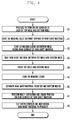
- FIG. 4 is a flowchart for describing a surface treatment method of an electronic device case according to an embodiment of the present disclosure.
- FIG. 5 illustrates a flow of a process for surface treatment of an electronic device case according to an embodiment of the present disclosure.
- FIG. 6 is a cross-sectional view of a process in which some steps in a process flow such as, for example, the process flow illustrated in FIG. 5 are illustrated as cross-sectional views according to an embodiment of the present disclosure.
- FIG. 7 is a view exemplifying a post process after a surface treatment of an electronic device case according to an embodiment of the present disclosure.
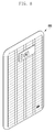
- FIG. 8 is a view illustrating an electronic device case which is a resultant item according to an embodiment of the present disclosure.
- the surface treatment method of an electronic device case may process a first pattern on one surface of a bottom mold 510 and a second pattern on one surface of a top mold 530.
- the bottom mold 510 and the top mold 530 may be respectively formed with a first pattern and a second pattern, on one surface of each of them, through an electroforming process to have a relief form, an intaglio form or a mixed form thereof formed through electroforming.
- the first pattern and the second pattern may be formed on the whole or a part of the bottom mold 510 and the top mold 530, respectively.
- the first pattern and the second pattern may be at least one of a check pattern, a hologram (interference pattern), a spin (rotary pattern), a hairline (stripe pattern), and/or the like.
- a UV molding liquid 520 may be coated on the front surface of the raw sheet material 500.
- the UV molding liquid 520 refers to a material which may act on a photochemical reaction by a UV energy (e.g., a UV ray having a wavelength of 100nm to 400nm) to be cured from a liquid phase to a solid phase and dried.
- a UV energy e.g., a UV ray having a wavelength of 100nm to 400nm
- the UV molding liquid 520 may be instantly cured by instant illumination of UV rays and may form a very excellent film.
- the UV molding liquid 520 may include of a photo-polymerizable resin (e.g., an oligomer and a reactive diluent), a photo-polymerization initiator, a pigment, auxiliary agents (e.g., a viscosity improvement agent, an oxidation inhibitor, a wetting agent, and a dispersion agent), a polymerization agent, and a sensitizer.
- a photo-polymerizable resin e.g., an oligomer and a reactive diluent
- auxiliary agents e.g., a viscosity improvement agent, an oxidation inhibitor, a wetting agent, and a dispersion agent
- the UV molding liquid 520 may consist of a photo-polymerizable resin (e.g., an oligomer and a reactive diluent), a photo-polymerization initiator, a pigment, auxiliary agents (e.g., a viscosity improvement agent, an oxidation inhibitor, a wetting agent, and a dispersion agent), a polymerization agent, and a sensitizer.
- a photo-polymerizable resin e.g., an oligomer and a reactive diluent
- auxiliary agents e.g., a viscosity improvement agent, an oxidation inhibitor, a wetting agent, and a dispersion agent
- the bottom mold 510 may be coated with the UV molding liquid 520.
- the UV molding liquid 520 may be coated on the bottom mold 510 where the check pattern 512 is carved.
- the raw sheet material 500 may be seated (e.g., disposed) in a space between the top mold 530 and the bottom mold 510.
- the raw sheet material 500 may be positioned in such a manner that the rear surface of the raw sheet material 500 faces the bottom mold 510 coated with the UV molding liquid 520 and the front surface of the raw sheet material 500 faces the surface of the top mold 530 formed with the second pattern.
- the top mold 530 and the bottom mold 510 may be pressed to each other.
- the UV molding liquid 520 coated on the front surface of the raw sheet material 500 and one surface of the top mold 530 are adhered to each other and the UV molding liquid 520 coated on one surface of the bottom mold 510 and the rear surface of the raw sheet material 500 may be adhered to each other.
- the UV molding liquid 522 may be adhered to the rear surface of the raw sheet material 500 as the check pattern and the UV molding liquid 524 may be adhered to the front surface of the raw sheet material 500 as the hairline.
- the UV molding liquid may be evenly distributed and occurrence of a positional deviation, which may be caused when the patterns desired to be formed on the front surface and the rear surface raw of the sheet material 500 are shifted or pushed out, may be suppressed, thereby ensuring that the patterns of the front surface and the rear surface may have uniformity.
- the surface treatment method forms the patterns on the raw sheet material without moving the raw sheet material in order to form the patterns by simultaneously pressing the top and bottom molds. As a result, a factor, which causes a surface appearance to go bad due to inclusion of foreign matter during the movement of the raw sheet material, may be prevented.
- the UV molding liquid 520 may be cured.
- the UV molding liquid 524 adhered to the front surface and the UV molding liquid 522 adhered to the rear surface raw of the sheet material 500 may be strongly bonded to the sheet material 500.
- Each of the top mold 530 and the bottom mold 510 may include a UV Light Emitting Diodes(LED) at a part thereof.
- each of the top mold 530 and the bottom mold 510 may be mounted with a UV LED in the form of a UV lamp 550 at each side thereof.
- the UV lamps 550 may be operated to cure the UV molding liquid.
- the curing condition for a process may be standardized.
- the light emitted from the UV lamps 550 may be reflected (e.g., totally reflected) to the raw sheet material in the state in which the top mold 530 and the bottom mold 510 are pressed to each other so that the UV molding liquid 520 may be evenly cured.
- the hairline that makes the front surface of the raw sheet material 500 have a texture and the check pattern 512 that makes the rear surface of raw sheet material 500 have a feeling of depth may be simultaneously formed.
- the raw sheet material 500 may be separated from the top mold 530 and the bottom mold 510.
- the sheet material 500 given an esthetic sense (e.g., look and feel) and a three-dimensional effect may be formed.
- a multi-deposition and black printing may be performed on the rear surface of the raw sheet material 500.
- the multi-deposition may be performed in a chamber in which the color of the raw sheet material 500 may be determined depending on a medium of the rear surface of the raw sheet material 500 and a pigment added thereto. By applying such a multi-deposition, various colors may be implemented on the raw sheet material 500.
- a printing layer may be formed on the rear surface of the raw sheet material 500 so as to implement a mirror-like effect on the front surface of the raw sheet material 500, and the visibility of the check pattern formed on the rear surface 210 of the raw sheet material may be further enhanced.
- a light transmission/interruption function may be implemented through the printing. At least one of mechanical machining using an NC machine, or a CNC machine, laser machining, pressing machining, and/or the like is performed to cut an outer contour line of the raw sheet material 500 formed through the above-described procedure. As a result, a UV molding applied deco may be obtained.
- an outer contour line may be cut and the raw sheet material 500 may be fastened to the product.
- an electronic device case may be formed when the UV molding applied deco 730 is attached or fastened to an electronic device case 710 using a tape 720, bonding, and/or the like.
- an electronic device case 800 may be completed.
- FIG. 7 illustrates a process of attaching the UV molding applied deco 730 to the electronic device case 710 through outserting.
- a method according to an embodiment of the present disclosure may perform an insert (so-called "IML") injection molding process as follows: the raw sheet material is inserted into a space between the top and bottom molds and then, the top and bottom molds are pressed by a press while a synthetic resin is introduced into the space between the top and bottom molds so that a resin layer is laminated on the rear surface of the machined raw sheet material in the space between the top and bottom molds, thereby molding an injection molded product as an electronic device case.
- IML insert
- a method according to an embodiment of the present disclosure may perform an inmold (so-called "IMD”) injection molding process as follows: the machined raw sheet material is inserted into a space between the top and bottom molds, a cylinder filled with a resin is connected to a press and then, the cylinder is compressed to introduce the resin within the cylinder into the space between the top and bottom mold while the molds are being pressed by the press.
- IMD inmold
- Various embodiments of the present disclosure simultaneously process the front surface and the rear surface of a raw sheet material in order to form patterns on an electronic device case. As a result, a process time may be shortened to increase a producing amount and to reduce a cost.
- Various embodiments of present disclosure press the top mold and the bottom mold so as to simultaneously form patterns on the front surface and the rear surface of a raw sheet material.
- the UV molding liquid may be evenly distributed, occurrence of a positional deviation between the front surface and the rear surface may be prevented, and a factor, which causes a surface appearance to go bad due to inclusion of foreign matter during the movement of the raw sheet material, may also be prevented.
- Various embodiments of the present disclosure mounts UV lamps on molds and the UV molding liquid may be cured using a phenomenon of the light emitted from the UV lamps being totally reflected to the raw sheet material when the molds are closed. As a result, a curing condition for a process may be standardized.
- the electronic device case includes a case body 710 and a deco 730 attached to the case body 710.
- the deco 730 may be made of a raw sheet material which includes, on an outwardly exposed surface thereof, a first pattern exhibiting a texture based on a relief form, an intaglio form, a mixed form thereof, or the like, and, on a rear surface thereof, a second pattern overlapped with the first pattern on a vertical line to express a feeling of depth.
- the first pattern is formed on one exposed side of the raw sheet material as a hairline and the second pattern is formed on the other side of the raw sheet material as a check pattern, in which the first and second patterns may be made of a UV molding liquid cured on each side of the raw sheet material.
- An adhesive layer 720 may be further included between the case body 710 and the deco 730 in which the adhesive layer 720 is made of at least one of a tape, bonding and a synthetic resin.
Landscapes
- Engineering & Computer Science (AREA)
- Mechanical Engineering (AREA)
- Physics & Mathematics (AREA)
- Health & Medical Sciences (AREA)
- Oral & Maxillofacial Surgery (AREA)
- Toxicology (AREA)
- Thermal Sciences (AREA)
- General Physics & Mathematics (AREA)
- Microelectronics & Electronic Packaging (AREA)
- Manufacturing & Machinery (AREA)
- Electromagnetism (AREA)
- Injection Moulding Of Plastics Or The Like (AREA)
- Laminated Bodies (AREA)
Applications Claiming Priority (1)
| Application Number | Priority Date | Filing Date | Title |
|---|---|---|---|
| KR1020130062370A KR20140141815A (ko) | 2013-05-31 | 2013-05-31 | 전자기기용 케이스 및 이의 표면 처리방법 |
Publications (2)
| Publication Number | Publication Date |
|---|---|
| EP2808150A1 EP2808150A1 (en) | 2014-12-03 |
| EP2808150B1 true EP2808150B1 (en) | 2016-02-17 |
Family
ID=50897361
Family Applications (1)
| Application Number | Title | Priority Date | Filing Date |
|---|---|---|---|
| EP14169745.8A Active EP2808150B1 (en) | 2013-05-31 | 2014-05-23 | Surface treatment method of an electronic device case |
Country Status (3)
| Country | Link |
|---|---|
| US (1) | US10082732B2 (ko) |
| EP (1) | EP2808150B1 (ko) |
| KR (1) | KR20140141815A (ko) |
Families Citing this family (7)
| Publication number | Priority date | Publication date | Assignee | Title |
|---|---|---|---|---|
| CN104441408A (zh) * | 2013-09-13 | 2015-03-25 | 联想(北京)有限公司 | 壳体的制备方法以及电子设备 |
| US10180248B2 (en) | 2015-09-02 | 2019-01-15 | ProPhotonix Limited | LED lamp with sensing capabilities |
| EP3576919B1 (en) * | 2017-04-24 | 2020-06-17 | NIKE Innovate C.V. | Transparent tooling mold and process for uv radiation curable rubber |
| WO2020023049A1 (en) * | 2018-07-27 | 2020-01-30 | Hewlett-Packard Development Company, L.P. | Surface decoration films |
| WO2021082443A1 (zh) * | 2019-11-01 | 2021-05-06 | Oppo广东移动通信有限公司 | 电子设备壳体及其制备方法和电子设备 |
| CN112045945A (zh) * | 2020-08-14 | 2020-12-08 | Oppo广东移动通信有限公司 | 电池盖、壳体组件、电子设备及成型模具 |
| CN114012953B (zh) * | 2021-11-02 | 2024-01-09 | 东莞正广精密科技有限公司 | 用液晶制作手机后壳的加工工艺 |
Family Cites Families (19)
| Publication number | Priority date | Publication date | Assignee | Title |
|---|---|---|---|---|
| US4110139A (en) * | 1974-03-13 | 1978-08-29 | Nco Works Ltd. | Process for preparing bands or belts, particularly suitable for use as watch bands |
| US4643787A (en) * | 1985-05-03 | 1987-02-17 | Versatube Corporation | Method of making an embossed panel door |
| CN1191578C (zh) * | 1999-05-17 | 2005-03-02 | 索尼株式会社 | 盘状多层记录媒体及其制造方法 |
| EP1233007B1 (en) * | 1999-07-01 | 2008-06-18 | Sekisui Chemical Co., Ltd. | Interlayer for Laminated Glass |
| US20020074692A1 (en) * | 2000-12-19 | 2002-06-20 | Ming-Ling Wang | Bathmat and the method for manufacturing the same |
| JP3580280B2 (ja) * | 2001-10-25 | 2004-10-20 | 株式会社日立製作所 | 記録媒体とその製造方法 |
| US7245406B2 (en) * | 2003-09-17 | 2007-07-17 | Dai Nippon Printing Co., Ltd. | Method for forming fine concavo-convex patterns, method for producing optical diffraction structure, and method for copying optical diffraction structure |
| JP4227587B2 (ja) * | 2004-11-11 | 2009-02-18 | 黒田 暢夫 | 合成樹脂製立体装飾片とその製造方法 |
| JP4861400B2 (ja) * | 2005-03-09 | 2012-01-25 | スリーエム イノベイティブ プロパティズ カンパニー | 位置合わせされた両面パターン化ウェブの作製装置および方法 |
| US8024016B2 (en) | 2006-07-18 | 2011-09-20 | Lg Electronics Inc. | Portable electronic device |
| US8377361B2 (en) * | 2006-11-28 | 2013-02-19 | Wei Zhang | Imprint lithography with improved substrate/mold separation |
| TWI315538B (en) | 2007-03-14 | 2009-10-01 | Ichia Tech Inc | Manufacturing method of thin keypad assembly |
| JP4482047B2 (ja) * | 2008-03-28 | 2010-06-16 | 株式会社東芝 | インプリント方法 |
| JP2010020842A (ja) * | 2008-07-10 | 2010-01-28 | Nec Corp | 微細パターン形成方法及び構造体の製造方法 |
| JP5638523B2 (ja) * | 2008-07-17 | 2014-12-10 | エージェンシー・フォー・サイエンス・テクノロジー・アンド・リサーチ | ポリマー構造上にインプリントを作製する方法 |
| JP5416420B2 (ja) * | 2009-01-22 | 2014-02-12 | 株式会社日立ハイテクノロジーズ | 微細構造転写装置 |
| US7954546B2 (en) | 2009-03-06 | 2011-06-07 | Baker Hughes Incorporated | Subterranean screen with varying resistance to flow |
| US8303880B2 (en) * | 2009-09-08 | 2012-11-06 | Shui Yuan Ma | Process of manufacturing a plastic product with decorated surfaces |
| US20110242847A1 (en) * | 2010-04-06 | 2011-10-06 | Skc Haas Display Films Co., Ltd. | Laminated double-sided light guide plate |
-
2013
- 2013-05-31 KR KR1020130062370A patent/KR20140141815A/ko not_active Ceased
-
2014
- 2014-05-19 US US14/280,900 patent/US10082732B2/en active Active
- 2014-05-23 EP EP14169745.8A patent/EP2808150B1/en active Active
Also Published As
| Publication number | Publication date |
|---|---|
| US10082732B2 (en) | 2018-09-25 |
| EP2808150A1 (en) | 2014-12-03 |
| US20140356563A1 (en) | 2014-12-04 |
| KR20140141815A (ko) | 2014-12-11 |
Similar Documents
| Publication | Publication Date | Title |
|---|---|---|
| EP2808150B1 (en) | Surface treatment method of an electronic device case | |
| US10875222B2 (en) | Plastic moulded part and method for the production thereof | |
| US10926440B2 (en) | Laminate sheet and molded body, and methods for producing the same | |
| EP2277678B1 (en) | Exterior component | |
| US20100156001A1 (en) | Method of combining laser-engraving and in-mold decoration techniques to laser-engrave pattern on plastic product and the product thereof | |
| KR101347187B1 (ko) | 발광 버튼키의 제조방법 | |
| US20130269862A1 (en) | Method of fabricating in-mold release film | |
| CN106738610A (zh) | 钢化玻璃与塑胶件的复合结构及其制造方法 | |
| CN113195193A (zh) | 装饰成形体、装饰成形体的制造方法以及使用装饰成形体的加工件的制造方法 | |
| JP2018501135A (ja) | 複合体の製造方法及び複合体 | |
| CN107465773A (zh) | 一种手机复合式玻璃后盖板的制作方法 | |
| CN203391497U (zh) | 模内转印箔 | |
| CN111193819B (zh) | 一种手机保护套及其生产工艺 | |
| JP6242677B2 (ja) | 立体エンブレムの製造方法 | |
| KR102111277B1 (ko) | 리얼 무늬 패턴이 형성된 판상부재 및 이의 제조방법 | |
| KR20150017845A (ko) | 알루미늄 박막이 부착된 차량용 천연소재 내장재 및 그 제조방법 | |
| KR102033683B1 (ko) | 두께감 및 메탈감을 갖는 고광택 문양 구현이 가능한 데코필름 제조방법 및 그 데코필름 | |
| KR20200035927A (ko) | 전자기기용 케이스 및 이의 표면 처리방법 | |
| JP2015120457A (ja) | 立体エンブレムの製造方法 | |
| CN106163820A (zh) | 用于印刷装饰图案的方法 | |
| JP2006281601A (ja) | 加飾成形品の製造方法 | |
| KR102321992B1 (ko) | 3d 코팅층이 형성된 엠블럼 제조방법 | |
| KR101835454B1 (ko) | 발포층 사이에 금속층이 형성된 버튼키 및 그 제조방법 | |
| KR20170084486A (ko) | 리얼카본 제품 및 이의 제조방법 | |
| KR20240176961A (ko) | 장식물 라벨 및 장식물 라벨 제작/부착 방법 |
Legal Events
| Date | Code | Title | Description |
|---|---|---|---|
| PUAI | Public reference made under article 153(3) epc to a published international application that has entered the european phase |
Free format text: ORIGINAL CODE: 0009012 |
|
| 17P | Request for examination filed |
Effective date: 20140523 |
|
| AK | Designated contracting states |
Kind code of ref document: A1 Designated state(s): AL AT BE BG CH CY CZ DE DK EE ES FI FR GB GR HR HU IE IS IT LI LT LU LV MC MK MT NL NO PL PT RO RS SE SI SK SM TR |
|
| AX | Request for extension of the european patent |
Extension state: BA ME |
|
| R17P | Request for examination filed (corrected) |
Effective date: 20150603 |
|
| RBV | Designated contracting states (corrected) |
Designated state(s): AL AT BE BG CH CY CZ DE DK EE ES FI FR GB GR HR HU IE IS IT LI LT LU LV MC MK MT NL NO PL PT RO RS SE SI SK SM TR |
|
| GRAP | Despatch of communication of intention to grant a patent |
Free format text: ORIGINAL CODE: EPIDOSNIGR1 |
|
| INTG | Intention to grant announced |
Effective date: 20150805 |
|
| GRAS | Grant fee paid |
Free format text: ORIGINAL CODE: EPIDOSNIGR3 |
|
| GRAA | (expected) grant |
Free format text: ORIGINAL CODE: 0009210 |
|
| AK | Designated contracting states |
Kind code of ref document: B1 Designated state(s): AL AT BE BG CH CY CZ DE DK EE ES FI FR GB GR HR HU IE IS IT LI LT LU LV MC MK MT NL NO PL PT RO RS SE SI SK SM TR |
|
| REG | Reference to a national code |
Ref country code: GB Ref legal event code: FG4D |
|
| REG | Reference to a national code |
Ref country code: CH Ref legal event code: EP |
|
| REG | Reference to a national code |
Ref country code: IE Ref legal event code: FG4D |
|
| REG | Reference to a national code |
Ref country code: AT Ref legal event code: REF Ref document number: 775427 Country of ref document: AT Kind code of ref document: T Effective date: 20160315 |
|
| REG | Reference to a national code |
Ref country code: DE Ref legal event code: R096 Ref document number: 602014000899 Country of ref document: DE |
|
| REG | Reference to a national code |
Ref country code: NL Ref legal event code: FP |
|
| REG | Reference to a national code |
Ref country code: LT Ref legal event code: MG4D |
|
| REG | Reference to a national code |
Ref country code: AT Ref legal event code: MK05 Ref document number: 775427 Country of ref document: AT Kind code of ref document: T Effective date: 20160217 |
|
| PG25 | Lapsed in a contracting state [announced via postgrant information from national office to epo] |
Ref country code: FI Free format text: LAPSE BECAUSE OF FAILURE TO SUBMIT A TRANSLATION OF THE DESCRIPTION OR TO PAY THE FEE WITHIN THE PRESCRIBED TIME-LIMIT Effective date: 20160217 Ref country code: HR Free format text: LAPSE BECAUSE OF FAILURE TO SUBMIT A TRANSLATION OF THE DESCRIPTION OR TO PAY THE FEE WITHIN THE PRESCRIBED TIME-LIMIT Effective date: 20160217 Ref country code: IT Free format text: LAPSE BECAUSE OF FAILURE TO SUBMIT A TRANSLATION OF THE DESCRIPTION OR TO PAY THE FEE WITHIN THE PRESCRIBED TIME-LIMIT Effective date: 20160217 Ref country code: ES Free format text: LAPSE BECAUSE OF FAILURE TO SUBMIT A TRANSLATION OF THE DESCRIPTION OR TO PAY THE FEE WITHIN THE PRESCRIBED TIME-LIMIT Effective date: 20160217 Ref country code: NO Free format text: LAPSE BECAUSE OF FAILURE TO SUBMIT A TRANSLATION OF THE DESCRIPTION OR TO PAY THE FEE WITHIN THE PRESCRIBED TIME-LIMIT Effective date: 20160517 |
|
| PG25 | Lapsed in a contracting state [announced via postgrant information from national office to epo] |
Ref country code: SE Free format text: LAPSE BECAUSE OF FAILURE TO SUBMIT A TRANSLATION OF THE DESCRIPTION OR TO PAY THE FEE WITHIN THE PRESCRIBED TIME-LIMIT Effective date: 20160217 Ref country code: LT Free format text: LAPSE BECAUSE OF FAILURE TO SUBMIT A TRANSLATION OF THE DESCRIPTION OR TO PAY THE FEE WITHIN THE PRESCRIBED TIME-LIMIT Effective date: 20160217 Ref country code: BE Free format text: LAPSE BECAUSE OF NON-PAYMENT OF DUE FEES Effective date: 20160531 Ref country code: RS Free format text: LAPSE BECAUSE OF FAILURE TO SUBMIT A TRANSLATION OF THE DESCRIPTION OR TO PAY THE FEE WITHIN THE PRESCRIBED TIME-LIMIT Effective date: 20160217 Ref country code: PL Free format text: LAPSE BECAUSE OF FAILURE TO SUBMIT A TRANSLATION OF THE DESCRIPTION OR TO PAY THE FEE WITHIN THE PRESCRIBED TIME-LIMIT Effective date: 20160217 Ref country code: PT Free format text: LAPSE BECAUSE OF FAILURE TO SUBMIT A TRANSLATION OF THE DESCRIPTION OR TO PAY THE FEE WITHIN THE PRESCRIBED TIME-LIMIT Effective date: 20160617 Ref country code: AT Free format text: LAPSE BECAUSE OF FAILURE TO SUBMIT A TRANSLATION OF THE DESCRIPTION OR TO PAY THE FEE WITHIN THE PRESCRIBED TIME-LIMIT Effective date: 20160217 Ref country code: LV Free format text: LAPSE BECAUSE OF FAILURE TO SUBMIT A TRANSLATION OF THE DESCRIPTION OR TO PAY THE FEE WITHIN THE PRESCRIBED TIME-LIMIT Effective date: 20160217 |
|
| PG25 | Lapsed in a contracting state [announced via postgrant information from national office to epo] |
Ref country code: EE Free format text: LAPSE BECAUSE OF FAILURE TO SUBMIT A TRANSLATION OF THE DESCRIPTION OR TO PAY THE FEE WITHIN THE PRESCRIBED TIME-LIMIT Effective date: 20160217 Ref country code: DK Free format text: LAPSE BECAUSE OF FAILURE TO SUBMIT A TRANSLATION OF THE DESCRIPTION OR TO PAY THE FEE WITHIN THE PRESCRIBED TIME-LIMIT Effective date: 20160217 |
|
| REG | Reference to a national code |
Ref country code: DE Ref legal event code: R097 Ref document number: 602014000899 Country of ref document: DE |
|
| PG25 | Lapsed in a contracting state [announced via postgrant information from national office to epo] |
Ref country code: RO Free format text: LAPSE BECAUSE OF FAILURE TO SUBMIT A TRANSLATION OF THE DESCRIPTION OR TO PAY THE FEE WITHIN THE PRESCRIBED TIME-LIMIT Effective date: 20160217 Ref country code: SK Free format text: LAPSE BECAUSE OF FAILURE TO SUBMIT A TRANSLATION OF THE DESCRIPTION OR TO PAY THE FEE WITHIN THE PRESCRIBED TIME-LIMIT Effective date: 20160217 Ref country code: SM Free format text: LAPSE BECAUSE OF FAILURE TO SUBMIT A TRANSLATION OF THE DESCRIPTION OR TO PAY THE FEE WITHIN THE PRESCRIBED TIME-LIMIT Effective date: 20160217 Ref country code: CZ Free format text: LAPSE BECAUSE OF FAILURE TO SUBMIT A TRANSLATION OF THE DESCRIPTION OR TO PAY THE FEE WITHIN THE PRESCRIBED TIME-LIMIT Effective date: 20160217 |
|
| PLBE | No opposition filed within time limit |
Free format text: ORIGINAL CODE: 0009261 |
|
| STAA | Information on the status of an ep patent application or granted ep patent |
Free format text: STATUS: NO OPPOSITION FILED WITHIN TIME LIMIT |
|
| PG25 | Lapsed in a contracting state [announced via postgrant information from national office to epo] |
Ref country code: LU Free format text: LAPSE BECAUSE OF FAILURE TO SUBMIT A TRANSLATION OF THE DESCRIPTION OR TO PAY THE FEE WITHIN THE PRESCRIBED TIME-LIMIT Effective date: 20160523 Ref country code: BE Free format text: LAPSE BECAUSE OF FAILURE TO SUBMIT A TRANSLATION OF THE DESCRIPTION OR TO PAY THE FEE WITHIN THE PRESCRIBED TIME-LIMIT Effective date: 20160217 |
|
| 26N | No opposition filed |
Effective date: 20161118 |
|
| REG | Reference to a national code |
Ref country code: IE Ref legal event code: MM4A |
|
| PG25 | Lapsed in a contracting state [announced via postgrant information from national office to epo] |
Ref country code: BG Free format text: LAPSE BECAUSE OF FAILURE TO SUBMIT A TRANSLATION OF THE DESCRIPTION OR TO PAY THE FEE WITHIN THE PRESCRIBED TIME-LIMIT Effective date: 20160517 Ref country code: SI Free format text: LAPSE BECAUSE OF FAILURE TO SUBMIT A TRANSLATION OF THE DESCRIPTION OR TO PAY THE FEE WITHIN THE PRESCRIBED TIME-LIMIT Effective date: 20160217 |
|
| REG | Reference to a national code |
Ref country code: FR Ref legal event code: ST Effective date: 20170131 |
|
| PG25 | Lapsed in a contracting state [announced via postgrant information from national office to epo] |
Ref country code: FR Free format text: LAPSE BECAUSE OF NON-PAYMENT OF DUE FEES Effective date: 20160531 |
|
| PG25 | Lapsed in a contracting state [announced via postgrant information from national office to epo] |
Ref country code: IE Free format text: LAPSE BECAUSE OF NON-PAYMENT OF DUE FEES Effective date: 20160523 |
|
| REG | Reference to a national code |
Ref country code: CH Ref legal event code: PL |
|
| PG25 | Lapsed in a contracting state [announced via postgrant information from national office to epo] |
Ref country code: LI Free format text: LAPSE BECAUSE OF NON-PAYMENT OF DUE FEES Effective date: 20170531 Ref country code: CH Free format text: LAPSE BECAUSE OF NON-PAYMENT OF DUE FEES Effective date: 20170531 |
|
| PG25 | Lapsed in a contracting state [announced via postgrant information from national office to epo] |
Ref country code: HU Free format text: LAPSE BECAUSE OF FAILURE TO SUBMIT A TRANSLATION OF THE DESCRIPTION OR TO PAY THE FEE WITHIN THE PRESCRIBED TIME-LIMIT; INVALID AB INITIO Effective date: 20140523 |
|
| PG25 | Lapsed in a contracting state [announced via postgrant information from national office to epo] |
Ref country code: CY Free format text: LAPSE BECAUSE OF FAILURE TO SUBMIT A TRANSLATION OF THE DESCRIPTION OR TO PAY THE FEE WITHIN THE PRESCRIBED TIME-LIMIT Effective date: 20160217 Ref country code: IS Free format text: LAPSE BECAUSE OF FAILURE TO SUBMIT A TRANSLATION OF THE DESCRIPTION OR TO PAY THE FEE WITHIN THE PRESCRIBED TIME-LIMIT Effective date: 20160217 Ref country code: MK Free format text: LAPSE BECAUSE OF FAILURE TO SUBMIT A TRANSLATION OF THE DESCRIPTION OR TO PAY THE FEE WITHIN THE PRESCRIBED TIME-LIMIT Effective date: 20160217 Ref country code: GR Free format text: LAPSE BECAUSE OF FAILURE TO SUBMIT A TRANSLATION OF THE DESCRIPTION OR TO PAY THE FEE WITHIN THE PRESCRIBED TIME-LIMIT Effective date: 20160217 Ref country code: MC Free format text: LAPSE BECAUSE OF FAILURE TO SUBMIT A TRANSLATION OF THE DESCRIPTION OR TO PAY THE FEE WITHIN THE PRESCRIBED TIME-LIMIT Effective date: 20160217 Ref country code: MT Free format text: LAPSE BECAUSE OF NON-PAYMENT OF DUE FEES Effective date: 20160531 |
|
| PG25 | Lapsed in a contracting state [announced via postgrant information from national office to epo] |
Ref country code: TR Free format text: LAPSE BECAUSE OF FAILURE TO SUBMIT A TRANSLATION OF THE DESCRIPTION OR TO PAY THE FEE WITHIN THE PRESCRIBED TIME-LIMIT Effective date: 20160217 Ref country code: AL Free format text: LAPSE BECAUSE OF FAILURE TO SUBMIT A TRANSLATION OF THE DESCRIPTION OR TO PAY THE FEE WITHIN THE PRESCRIBED TIME-LIMIT Effective date: 20160217 |
|
| PGFP | Annual fee paid to national office [announced via postgrant information from national office to epo] |
Ref country code: NL Payment date: 20230421 Year of fee payment: 10 |
|
| PGFP | Annual fee paid to national office [announced via postgrant information from national office to epo] |
Ref country code: GB Payment date: 20230420 Year of fee payment: 10 |
|
| REG | Reference to a national code |
Ref country code: NL Ref legal event code: MM Effective date: 20240601 |
|
| GBPC | Gb: european patent ceased through non-payment of renewal fee |
Effective date: 20240523 |
|
| PG25 | Lapsed in a contracting state [announced via postgrant information from national office to epo] |
Ref country code: NL Free format text: LAPSE BECAUSE OF NON-PAYMENT OF DUE FEES Effective date: 20240601 |
|
| PG25 | Lapsed in a contracting state [announced via postgrant information from national office to epo] |
Ref country code: GB Free format text: LAPSE BECAUSE OF NON-PAYMENT OF DUE FEES Effective date: 20240523 |
|
| PGFP | Annual fee paid to national office [announced via postgrant information from national office to epo] |
Ref country code: DE Payment date: 20250422 Year of fee payment: 12 |