EP2808754A1 - Elektronische Vorrichtung - Google Patents
Elektronische Vorrichtung Download PDFInfo
- Publication number
- EP2808754A1 EP2808754A1 EP13191311.3A EP13191311A EP2808754A1 EP 2808754 A1 EP2808754 A1 EP 2808754A1 EP 13191311 A EP13191311 A EP 13191311A EP 2808754 A1 EP2808754 A1 EP 2808754A1
- Authority
- EP
- European Patent Office
- Prior art keywords
- main unit
- display unit
- keyboard
- state
- hinge
- Prior art date
- Legal status (The legal status is an assumption and is not a legal conclusion. Google has not performed a legal analysis and makes no representation as to the accuracy of the status listed.)
- Withdrawn
Links
Images







Classifications
-
- G—PHYSICS
- G06—COMPUTING OR CALCULATING; COUNTING
- G06F—ELECTRIC DIGITAL DATA PROCESSING
- G06F1/00—Details not covered by groups G06F3/00 - G06F13/00 and G06F21/00
- G06F1/16—Constructional details or arrangements
- G06F1/1613—Constructional details or arrangements for portable computers
- G06F1/1633—Constructional details or arrangements of portable computers not specific to the type of enclosures covered by groups G06F1/1615 - G06F1/1626
- G06F1/1637—Details related to the display arrangement, including those related to the mounting of the display in the housing
-
- G—PHYSICS
- G06—COMPUTING OR CALCULATING; COUNTING
- G06F—ELECTRIC DIGITAL DATA PROCESSING
- G06F1/00—Details not covered by groups G06F3/00 - G06F13/00 and G06F21/00
- G06F1/16—Constructional details or arrangements
- G06F1/1613—Constructional details or arrangements for portable computers
- G06F1/1615—Constructional details or arrangements for portable computers with several enclosures having relative motions, each enclosure supporting at least one I/O or computing function
- G06F1/1624—Constructional details or arrangements for portable computers with several enclosures having relative motions, each enclosure supporting at least one I/O or computing function with sliding enclosures, e.g. sliding keyboard or display
-
- G—PHYSICS
- G06—COMPUTING OR CALCULATING; COUNTING
- G06F—ELECTRIC DIGITAL DATA PROCESSING
- G06F1/00—Details not covered by groups G06F3/00 - G06F13/00 and G06F21/00
- G06F1/16—Constructional details or arrangements
- G06F1/1613—Constructional details or arrangements for portable computers
- G06F1/1633—Constructional details or arrangements of portable computers not specific to the type of enclosures covered by groups G06F1/1615 - G06F1/1626
- G06F1/1662—Details related to the integrated keyboard
Definitions
- the present disclosure relates to an electronic device.
- JP-A-2009-230244 describes an apparatus that slides and tilts up/down a display unit with respect to a main unit.
- This apparatus includes a main unit that has a keyboard on its upper face for inputting information, and a display unit that has on its upper face a display for displaying information.
- the apparatus slides and tilts up/down the display unit with respect to the main unit with a slide mechanism and a tilt up/down mechanism.
- an electronic device including a flat main unit provided with a keyboard, a flat display unit having a display face, the flat display unit configured to movably slide between a first state that overlaps the main unit and a second state that is erect with respect to the main unit, and a single hinge that is arranged so as to overlap the keyboard in the first state, and is configured to couple the main unit and the display unit together so that the display unit can move with respect to the main unit.
- the hinge may be arranged so as to extend toward a center in a width direction of the keyboard in the first state.
- a step may be provided so that an upper face of the keyboard is lower than an upper face of the main unit.
- a space may be formed between the main unit and a face of the display unit opposing the main unit.
- the hinge may be provided in the space.
- An upper face of the keyboard may be slanted with respect to an upper face of the main unit.
- the display unit may include a convex-shaped area on at least a part of a face opposing the main unit in the first state.
- the convex-shaped area may take up at least a part of the space, and a predetermined module is arranged in the convex-shaped area.
- the convex-shaped area may be arranged on either side of the hinge in the space.
- the predetermined module may include at least one of a circuit board on which an electronic part is mounted, a communication module, and a speaker.
- a pointing device may be provided at an area on a near side of the keyboard.
- the maximum possible space for the keyboard can be obtained, and the apparatus can be made more compact and thinner.
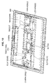
- FIGS. 1 to 3 are schematic diagrams illustrating the appearance of an information processing apparatus (electronic device) 1000.
- the information processing apparatus 1000 has a main unit 100 and a display unit 200.
- a keyboard 110 is provided on the main unit 100.
- the display unit 200 includes a touch panel 210 that is provided with a touch sensor on a display device such as a LCD.
- FIG. 1 illustrates a state in which the display unit 200 overlaps the display unit 200.
- the user can perform a desired operation by operating the touch panel 210.
- the user can use the information processing apparatus 1000 as a so-called tablet terminal.
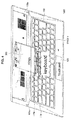
- FIG. 2 illustrates a state in which the display unit 200 has been slid up and is erect with respect to the main unit 100.
- the user can perform a desired operation by operating the keyboard 110.
- the user can also perform a desired operation by operating the touch panel 210 on the display unit 200.
- the user can also perform a desired operation by operating a touch pad 120, which is a pointing device provided on an area in front of the keyboard 110.
- FIG. 3 illustrates a state in which the state illustrated in FIG. 2 is viewed from a back face of the information processing apparatus 1000.
- the main unit 100 and the display unit 200 are connected via a hinge 300.
- the information processing apparatus 1000 can move between the state illustrated in FIG. 1 and the state illustrated in FIG. 2 by sliding the display unit 200 with respect to the main unit 100 via the hinge 300 (hereinafter also referred to as "surface-sliding").
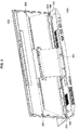
- FIG. 4 is a perspective diagram illustrating a state in which the display unit 200 has been removed from the state illustrated in FIG. 1 .
- a part of the near side of the hinge 300 overlaps the keyboard 110.
- the hinge 300 is provided extending toward a front side until it overlaps the keyboard 110 to ensure that the length of the hinge 300 in the front-rear direction is sufficiently long.
- FIG. 5 is a schematic diagram illustrating a link mechanism of the main unit 100, the display unit 200, and the hinge 300.
- the upper section of FIG. 5 schematically illustrates the state illustrated in FIG. 1
- the lower section schematically illustrates the state illustrated in FIG. 2 .
- a length L1 of the hinge 300 is long, so that the hinge 300 and the keyboard 110 overlap.
- the hinge 300 is configured from two hinge plates 310 and 320.
- the main unit 100 and the display unit 200 are connected via two links (joints) 330 and 340. Further, the main unit 100 and the display unit 200 are connected via two links (joints) 350 and 360. Based on such a configuration, when the display unit 200 is slid to the rear side of the main unit 100, the display unit 200 can be tilted with respect to the main unit 100.
- FIG. 6 illustrates an example in which a length L2 of the display unit 200 is shorter than the length L1 of the display unit 200 in FIG. 5 , so that the hinge 300 does not overlap the keyboard 110.
- the display unit 200 when the display unit 200 is tilted, since the length L2 of the hinge is short, the tilt angle is smaller than in FIG. 5 , so the display unit 200 faces upward. Consequently, the keyboard 110 is arranged toward the front of the main unit 100, which means that the size of the keyboard 110 is limited.
- the tilt angle can be sufficient increased. Consequently, in the state illustrated in FIG. 2 , the lower edge of the display unit 200 can be positioned further toward the back of the main unit 100, so that the keyboard 110 can be arranged further toward the back of the main unit 100. This enables constituent elements, such as a touch pad, a palm rest, and a NFC device, to be arranged in an area in front of the keyboard 110. Further, by increasing the tilt angle, the visibility of the display unit 200 can be increased when the user places the information processing apparatus 1000 on a desk and operates it in the state illustrated in FIG. 2 .
- the usage area of the keyboard 110 can be increased without the position of the keyboard 110 being restricted by the position of the hinge 300. Consequently, the key pitch can also be increased.
- the usage area of the hinge 300 widens, so that the lower edge of the display unit 200 can be moved as far as the back of the main unit 100 when in the state illustrated in FIG. 2 . Consequently, the tilt angle can be increased and the area of the keyboard 110 can be further widened.
- this also enables the keyboard 110 to be arranged further to the rear of the main unit 100. Therefore, as illustrated in FIG.
- the touch pad 120 can be arranged on the front side of the keyboard 110, and a NFC device, a palm rest and the like can also be arranged.
- a NFC device, a palm rest and the like can also be arranged.
- the hinge 300 is configured so as to not overlap the keyboard 110, this means that the keyboard 110 is arranged further to the front of the main unit 100, which makes it difficult to ensure a space to provide the touch pad 120. Therefore, by configuring like in the present embodiment so that the hinge 300 overlaps the keyboard 110, a useful space can be ensured on the front side of the keyboard 110, so that a configuration having a greater added value can be obtained.
- the hinge 300 is arranged at only one location in the center of the main unit 100. If, for example, the hinge 300 is arranged at two locations at either end of the main unit 100, a space for the hinges 300 would probably be provided at either end of the keyboard 110, meaning that the horizontal width of the main unit 100 would likely increase. Moreover, this may also mean that a concave portion, a groove or the like to avoid the hinges is provided on the main unit 100 at either end of the keyboard 110. Therefore, by arranging the hinge 300 at just one location in the center of the main unit 100, the information processing apparatus 1000 can be made as compact as possible, and the configuration of the information processing apparatus 1000 can be made simple so as to not harm the appearance.
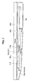
- FIG. 7 is a schematic diagram illustrating a cross-section along a front-rear direction of the center of the information processing apparatus 1000.
- an upper face 110a of the keyboard 110 is arranged at a predetermined angle with respect to an upper face 100a of the main unit 100.
- the upper face 100a of the main unit 100 and the upper face 110a of the keyboard 110 are not parallel. Consequently, as illustrated in FIG. 4 , a step between the upper face 110a of the keyboard 110 and the upper face 100a of the main unit 100 becomes greater and greater heading toward the back of the main unit 100.
- a predetermined space V is formed between the display unit 200 and the keyboard 110.
- the hinge 300 is arranged in this space V. Therefore, the hinge 300 can be housed in the space V without being interfered with by the keyboard 110 or the display unit 200.
- FIG. 8 is a cross-sectional view illustrating FIG. 7 in more detail. As illustrated in FIG. 8 , the hinge 300 is arranged in the space V between the keyboard 110 and the display unit 200.
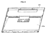
- FIG. 9 is a schematic diagram illustrating a convex-shaped area 200a provided on the rear side of the display unit 200. As illustrated in FIG. 9 , the bulge 200a is provided to the left and right of the center of the display unit 200. The bulge 200a is formed so that the thickness of the display unit 200 becomes thicker heading further back beyond the main unit 100 in the state illustrated in FIG. 1 to match the shape of the space V formed between the display unit 200 and the main unit 100.
- FIG. 10 is a schematic diagram illustrating an internal configuration of the display unit 200.
- a relay board 220 that combines three types of signal line into one from a touch panel board, a camera module, and a button board may be arranged on one convex-shaped area 200a.
- a board mounted with a WAN module and a SIM slot may be arranged on another convex-shaped area 200a.
- the convex-shaped area 200a can also be utilized without leaving any space by arranging an LCD harness, an antenna cable and the like on the convex-shaped area 200a.
- modules such as a speaker and a battery
- a speaker may also be arranged on the convex-shaped area 200a.
- a speaker is arranged on the convex-shaped area 200a, since a very large space can be used compared with the space on the main unit 100 side, a high audio quality speaker can be arranged. Compared with when arranged on the main unit 100, sound can be transmitted from a higher position, so that audio quality can be increased. Further, if a battery is arranged on the convex-shaped area 200a, the battery capacity can be increased.
- modules that are noise generation sources such as a motherboard, are arranged on the main unit 100. Consequently, it is desirable to arrange communication system modules, antennas and the like that are susceptible to the effects of noise on the convex-shaped area 200a of the display unit 200. This enables the effects of noise from the main unit 100 to be suppressed. If arranging an antenna, the antenna can also be effectively employed as a countermeasure against SAR. Further, a NFC (near field communication) device may also be mounted on the convex-shaped area 200a.
- NFC near field communication
- FIGS. 11 and 12 are schematic diagrams illustrating examples in which a module is arranged on the convex-shaped area 200a.
- FIG. 11 illustrates the state of FIG. 1 as viewed from above.
- FIG. 12 illustrates a cross-section along the dashed line III-III' in FIG. 11 , in which a cross-section further to the right side then the hinge 300 is shown.
- a WAN board 240 is arranged as a module on the convex-shaped area 200a on the right side of the display unit 200.
- Other modules can also be similarly arranged. Since the vertical width of the space V increases heading toward the back of the information processing apparatus 1000, it is preferred to arrange modules that are comparatively thick at the far side of the information processing apparatus 1000, and modules that are comparatively thin at the near side of the information processing apparatus 1000.
- the information processing apparatus 1000 can be made as small as possible by effectively utilizing the space V by arranging modules on the convex-shaped area 200a. These modules can be arranged without increasing the overall thickness of the information processing apparatus 1000. By arranging modules that would normally be arranged on the main unit 100 on the display unit 200 side, wasted space can be eliminated, and the information processing apparatus 1000 can be made more compact and lighter.
- the image processing apparatus 1000 can be made even more compact than when the hinge 300 is provided at either side of the main unit 100.
- the hinge 300 can be housed in this space V.
- the convex-shaped area 200a is provided on the face of the display unit 200 opposing the main unit 100, and the display unit 200 overlaps the main unit 100 (state illustrated in FIG.
- the convex-shaped area 200a of the display unit 200 takes up the space V, a predetermined module can be housed on the convex-shaped area 200a. Consequently, the space V can be effectively utilized, and the image processing apparatus 1000 can be made even more compact.
- present technology may also be configured as below.
Landscapes
- Engineering & Computer Science (AREA)
- Theoretical Computer Science (AREA)
- Computer Hardware Design (AREA)
- Physics & Mathematics (AREA)
- Human Computer Interaction (AREA)
- General Engineering & Computer Science (AREA)
- General Physics & Mathematics (AREA)
- Mathematical Physics (AREA)
- Casings For Electric Apparatus (AREA)
- Telephone Set Structure (AREA)
- Input From Keyboards Or The Like (AREA)
Applications Claiming Priority (1)
| Application Number | Priority Date | Filing Date | Title |
|---|---|---|---|
| JP2013112337A JP2014232387A (ja) | 2013-05-28 | 2013-05-28 | 電子機器 |
Publications (1)
| Publication Number | Publication Date |
|---|---|
| EP2808754A1 true EP2808754A1 (de) | 2014-12-03 |
Family
ID=49552187
Family Applications (1)
| Application Number | Title | Priority Date | Filing Date |
|---|---|---|---|
| EP13191311.3A Withdrawn EP2808754A1 (de) | 2013-05-28 | 2013-11-01 | Elektronische Vorrichtung |
Country Status (4)
| Country | Link |
|---|---|
| US (1) | US20140355186A1 (de) |
| EP (1) | EP2808754A1 (de) |
| JP (1) | JP2014232387A (de) |
| CN (2) | CN104216472A (de) |
Citations (3)
| Publication number | Priority date | Publication date | Assignee | Title |
|---|---|---|---|---|
| US6464195B1 (en) * | 1997-12-04 | 2002-10-15 | Raymond Hildebrandt | Ergonomic mounting for computer screen displays |
| JP2009230244A (ja) | 2008-03-19 | 2009-10-08 | Sony Corp | 携帯型情報処理装置 |
| EP2472347A2 (de) * | 2010-12-28 | 2012-07-04 | Sony Corporation | Vorrichtungsöffnungs- und -schießmechanismus und Informationsvorrichtung |
Family Cites Families (9)
| Publication number | Priority date | Publication date | Assignee | Title |
|---|---|---|---|---|
| US5668570A (en) * | 1993-06-29 | 1997-09-16 | Ditzik; Richard J. | Desktop computer with adjustable flat panel screen |
| US6870730B2 (en) * | 1995-09-26 | 2005-03-22 | Psion-Computers Plc | Computer with a pen or touch sensitive display |
| WO2003021408A2 (en) * | 2001-08-29 | 2003-03-13 | Danger, Inc. | Sliding display apparatus |
| US7239505B2 (en) * | 2004-10-08 | 2007-07-03 | Microsoft Corporation | Direct hinge for optimizing conversion |
| US7215538B1 (en) * | 2005-10-18 | 2007-05-08 | Shaofen Chen | Portable computer with multi-sectioned arms to support display position adjustment and multiple configurations |
| US20070217131A1 (en) * | 2006-03-15 | 2007-09-20 | Garry Kehr | Systems and methods for providing a movable computer display |
| TWI296883B (en) * | 2006-03-17 | 2008-05-11 | Htc Corp | Portable electronic device |
| JP2010157442A (ja) * | 2008-12-26 | 2010-07-15 | Sony Corp | 電子機器およびバッテリパック |
| JP6146138B2 (ja) * | 2013-05-28 | 2017-06-14 | ソニー株式会社 | 電子機器 |
-
2013
- 2013-05-28 JP JP2013112337A patent/JP2014232387A/ja active Pending
- 2013-10-28 US US14/064,473 patent/US20140355186A1/en not_active Abandoned
- 2013-11-01 EP EP13191311.3A patent/EP2808754A1/de not_active Withdrawn
-
2014
- 2014-05-23 CN CN201410219219.0A patent/CN104216472A/zh active Pending
- 2014-05-23 CN CN201420265104.0U patent/CN204288045U/zh not_active Expired - Fee Related
Patent Citations (3)
| Publication number | Priority date | Publication date | Assignee | Title |
|---|---|---|---|---|
| US6464195B1 (en) * | 1997-12-04 | 2002-10-15 | Raymond Hildebrandt | Ergonomic mounting for computer screen displays |
| JP2009230244A (ja) | 2008-03-19 | 2009-10-08 | Sony Corp | 携帯型情報処理装置 |
| EP2472347A2 (de) * | 2010-12-28 | 2012-07-04 | Sony Corporation | Vorrichtungsöffnungs- und -schießmechanismus und Informationsvorrichtung |
Also Published As
| Publication number | Publication date |
|---|---|
| US20140355186A1 (en) | 2014-12-04 |
| CN104216472A (zh) | 2014-12-17 |
| CN204288045U (zh) | 2015-04-22 |
| JP2014232387A (ja) | 2014-12-11 |
Similar Documents
| Publication | Publication Date | Title |
|---|---|---|
| US9229480B2 (en) | Electronic device having a display unit and a main unit rotatably connected together by a hinge | |
| EP2713585B1 (de) | Elektronische Vorrichtung und Steuerungsverfahren dafür | |
| EP2518979B1 (de) | Flexible Leiterplatte und mobiles Endgerät damit | |
| US9274557B2 (en) | Stand for electronic device and electronic device | |
| KR102042264B1 (ko) | 이동 단말기 | |
| US20140355210A1 (en) | Stand for electronic device and electronic device | |
| US9261928B2 (en) | Electronic device | |
| US9411364B2 (en) | Electronic assembly and electronic apparatus | |
| KR20120069365A (ko) | 이동 단말기 | |
| US9282668B2 (en) | Electronic apparatus and method for assembling the same | |
| JP6322908B2 (ja) | 表示装置および表示支持装置 | |
| EP2808754A1 (de) | Elektronische Vorrichtung | |
| US9119312B2 (en) | Support device and system | |
| JP4261399B2 (ja) | 携帯情報端末 | |
| KR20130091588A (ko) | 이동 단말기 | |
| JP5228919B2 (ja) | 携帯電子機器 | |
| KR101829062B1 (ko) | 슬림형 휴대 장치 | |
| US9013639B2 (en) | Electronic apparatus having a module protection buffer | |
| CN101668392A (zh) | 电子装置 | |
| JP5729943B2 (ja) | 情報処理装置 | |
| KR20130137987A (ko) | 이동 단말기 | |
| JP2015104002A (ja) | スライド型電子機器 |
Legal Events
| Date | Code | Title | Description |
|---|---|---|---|
| PUAI | Public reference made under article 153(3) epc to a published international application that has entered the european phase |
Free format text: ORIGINAL CODE: 0009012 |
|
| 17P | Request for examination filed |
Effective date: 20131101 |
|
| AK | Designated contracting states |
Kind code of ref document: A1 Designated state(s): AL AT BE BG CH CY CZ DE DK EE ES FI FR GB GR HR HU IE IS IT LI LT LU LV MC MK MT NL NO PL PT RO RS SE SI SK SM TR |
|
| AX | Request for extension of the european patent |
Extension state: BA ME |
|
| STAA | Information on the status of an ep patent application or granted ep patent |
Free format text: STATUS: THE APPLICATION HAS BEEN WITHDRAWN |
|
| 18W | Application withdrawn |
Effective date: 20160401 |