EP2808770B1 - Film conducteur monocouche pour commande tactile multipoint et son procédé de production - Google Patents
Film conducteur monocouche pour commande tactile multipoint et son procédé de production Download PDFInfo
- Publication number
- EP2808770B1 EP2808770B1 EP14166652.9A EP14166652A EP2808770B1 EP 2808770 B1 EP2808770 B1 EP 2808770B1 EP 14166652 A EP14166652 A EP 14166652A EP 2808770 B1 EP2808770 B1 EP 2808770B1
- Authority
- EP
- European Patent Office
- Prior art keywords
- layer
- module
- conductive film
- point touch
- transparent
- Prior art date
- Legal status (The legal status is an assumption and is not a legal conclusion. Google has not performed a legal analysis and makes no representation as to the accuracy of the status listed.)
- Not-in-force
Links
Images



Classifications
-
- G—PHYSICS
- G06—COMPUTING OR CALCULATING; COUNTING
- G06F—ELECTRIC DIGITAL DATA PROCESSING
- G06F3/00—Input arrangements for transferring data to be processed into a form capable of being handled by the computer; Output arrangements for transferring data from processing unit to output unit, e.g. interface arrangements
- G06F3/01—Input arrangements or combined input and output arrangements for interaction between user and computer
- G06F3/03—Arrangements for converting the position or the displacement of a member into a coded form
- G06F3/041—Digitisers, e.g. for touch screens or touch pads, characterised by the transducing means
-
- G—PHYSICS
- G06—COMPUTING OR CALCULATING; COUNTING
- G06F—ELECTRIC DIGITAL DATA PROCESSING
- G06F3/00—Input arrangements for transferring data to be processed into a form capable of being handled by the computer; Output arrangements for transferring data from processing unit to output unit, e.g. interface arrangements
- G06F3/01—Input arrangements or combined input and output arrangements for interaction between user and computer
- G06F3/03—Arrangements for converting the position or the displacement of a member into a coded form
- G06F3/041—Digitisers, e.g. for touch screens or touch pads, characterised by the transducing means
- G06F3/044—Digitisers, e.g. for touch screens or touch pads, characterised by the transducing means by capacitive means
- G06F3/0443—Digitisers, e.g. for touch screens or touch pads, characterised by the transducing means by capacitive means using a single layer of sensing electrodes
-
- G—PHYSICS
- G06—COMPUTING OR CALCULATING; COUNTING
- G06F—ELECTRIC DIGITAL DATA PROCESSING
- G06F3/00—Input arrangements for transferring data to be processed into a form capable of being handled by the computer; Output arrangements for transferring data from processing unit to output unit, e.g. interface arrangements
- G06F3/01—Input arrangements or combined input and output arrangements for interaction between user and computer
- G06F3/03—Arrangements for converting the position or the displacement of a member into a coded form
- G06F3/041—Digitisers, e.g. for touch screens or touch pads, characterised by the transducing means
- G06F3/044—Digitisers, e.g. for touch screens or touch pads, characterised by the transducing means by capacitive means
- G06F3/0446—Digitisers, e.g. for touch screens or touch pads, characterised by the transducing means by capacitive means using a grid-like structure of electrodes in at least two directions, e.g. using row and column electrodes
-
- G—PHYSICS
- G06—COMPUTING OR CALCULATING; COUNTING
- G06F—ELECTRIC DIGITAL DATA PROCESSING
- G06F3/00—Input arrangements for transferring data to be processed into a form capable of being handled by the computer; Output arrangements for transferring data from processing unit to output unit, e.g. interface arrangements
- G06F3/01—Input arrangements or combined input and output arrangements for interaction between user and computer
- G06F3/03—Arrangements for converting the position or the displacement of a member into a coded form
- G06F3/041—Digitisers, e.g. for touch screens or touch pads, characterised by the transducing means
- G06F3/044—Digitisers, e.g. for touch screens or touch pads, characterised by the transducing means by capacitive means
- G06F3/0448—Details of the electrode shape, e.g. for enhancing the detection of touches, for generating specific electric field shapes, for enhancing display quality
-
- H—ELECTRICITY
- H01—ELECTRIC ELEMENTS
- H01B—CABLES; CONDUCTORS; INSULATORS; SELECTION OF MATERIALS FOR THEIR CONDUCTIVE, INSULATING OR DIELECTRIC PROPERTIES
- H01B1/00—Conductors or conductive bodies characterised by the conductive materials; Selection of materials as conductors
- H01B1/02—Conductors or conductive bodies characterised by the conductive materials; Selection of materials as conductors mainly consisting of metals or alloys
-
- G—PHYSICS
- G06—COMPUTING OR CALCULATING; COUNTING
- G06F—ELECTRIC DIGITAL DATA PROCESSING
- G06F2203/00—Indexing scheme relating to G06F3/00 - G06F3/048
- G06F2203/041—Indexing scheme relating to G06F3/041 - G06F3/045
- G06F2203/04103—Manufacturing, i.e. details related to manufacturing processes specially suited for touch sensitive devices
-
- G—PHYSICS
- G06—COMPUTING OR CALCULATING; COUNTING
- G06F—ELECTRIC DIGITAL DATA PROCESSING
- G06F2203/00—Indexing scheme relating to G06F3/00 - G06F3/048
- G06F2203/041—Indexing scheme relating to G06F3/041 - G06F3/045
- G06F2203/04111—Cross over in capacitive digitiser, i.e. details of structures for connecting electrodes of the sensing pattern where the connections cross each other, e.g. bridge structures comprising an insulating layer, or vias through substrate
-
- Y—GENERAL TAGGING OF NEW TECHNOLOGICAL DEVELOPMENTS; GENERAL TAGGING OF CROSS-SECTIONAL TECHNOLOGIES SPANNING OVER SEVERAL SECTIONS OF THE IPC; TECHNICAL SUBJECTS COVERED BY FORMER USPC CROSS-REFERENCE ART COLLECTIONS [XRACs] AND DIGESTS
- Y10—TECHNICAL SUBJECTS COVERED BY FORMER USPC
- Y10T—TECHNICAL SUBJECTS COVERED BY FORMER US CLASSIFICATION
- Y10T428/00—Stock material or miscellaneous articles
- Y10T428/24—Structurally defined web or sheet [e.g., overall dimension, etc.]
- Y10T428/24479—Structurally defined web or sheet [e.g., overall dimension, etc.] including variation in thickness
- Y10T428/24612—Composite web or sheet
Definitions
- the present invention relates to a touch-control conductive film, and more particularly, to a single-layer multi-point touch-control conductive film and a method for producing the same.
- a transparent conductive film is a sensing element for receiving input signals, such as a touch in a touch screen.
- ITO Indium tin oxide
- technologies of manufacturing a touch-screen have been developed at a rather rapid speed, taking a projected capacitive screen as an example, the basic manufacturing process of the ITO layer has not changed much in recent years, ITO plating and ITO patterning are always unavoidable.
- ITO Indium is an expensive metallic material
- costs of the touch screen can be greatly increased when taking ITO as the material of the conductive layer.
- the whole plated ITO film needs to be etched to form ITO patterns, and therefore large amounts of ITO is etched away in this process, which leads to pollution and a waste of large amounts of precious metal.
- D1 discloses a transparent conduction film, a conduction 30 structure thereof and a preparation method of the transparent conduction film.
- the transparent conduction film is of a single-sided dual-layer conduction structure.
- the conduction structure comprises a first metal embedding layer and a second metal embedding layer, wherein the first metal embedding layer is formed by impressing on a substrate or impressing on a polymer sub-layer on the surface of the substrate; and the second metal embedding layer is formed by coating the polymer sub-layer on the surface of the first metal embedding layer through impressing, the first sub-layer of conduction structure and the second sub-layer of conduction structure have a grid groove structure, and conductive materials are filled in grooves.
- D2 discloses a structure of a bridging electrode, the structure of a bridging electrode applied to a capacitive touchpad, the structure comprising: a substrate; a plurality of first electrode blocks disposed on the substrate and electrically connected together in series through a first wire; a plurality of second electrode blocks disposed on the substrate and respectively disposed on two sides of the first wire; and a bridging insulation unit, which is perpendicular to and disposed on the first wire and having a bridging groove; wherein the second electrode blocks connecting electrically together in series through the bridging insulation unit having a second wire.
- a single-layer multi-point touch-control conductive film including:
- the above single-layer multi-point touch-control conductive film has at least advantages as follows:
- the transparent substrate is a transparent glass substrate.
- the bridging module is made of a metallic conductive material in a line shape with a line width range of 500 nm ⁇ 6 ⁇ m.
- the bridging module is made of a transparent conductive material.
- the conductive module is made of a transparent conductive material.
- the conductive module and the bridging module have transmittance of greater than 80%.
- the bridging module is a line segment, or a structure formed by two line segments being connected via at least one connecting line segment.
- the line segment has a width range of 1 ⁇ 6 ⁇ m.
- the conductive module when the bridging module is the line segment, the conductive module is provided on two ends of the line segment; when the bridging module is the structure formed by two line segments being connected via at least one connecting line segment, the conductive module is provided on the two line segments.
- the conductive module is in a line segment shape with a width range of 500 nm ⁇ 5 ⁇ m.
- the conductive film further comprises a light shielding sub-layer, located on an edge of the transparent glass substrate, and made of ink or black resist.
- the first electrode is a driving electrode
- the second electrode is an sensing electrode
- the single-layer multi-point conductive film further comprises a lead electrode, positioned at a non-viewing area of the single-layer multi-point touch-control conductive film, and the conductive material of the lead electrode is in electrical connection with the conductive material in the first groove-shaped grid.
- the surface edge of the transparent polymer sub-layer corresponding to the non-viewing area of the single-layer multi-point touch-control conductive film is formed with a second groove-shaped grid being filled with a conductive material to form the lead electrode.
- the first groove-shaped grid and the second groove-shaped grid are a regular grid or a random grid.
- the first groove-shaped grid and the second groove-shaped grid have a groove width of d1 and a depth of h, wherein 1 ⁇ m ⁇ d1 ⁇ 5 ⁇ m, 2 ⁇ m ⁇ h ⁇ 6 ⁇ m, h/d 1>1.
- the lead electrode is a grid-like or line-like conductive material formed on the transparent substrate or provided on the surface edge of the transparent polymer sub-layer, and arranged corresponding to the non-viewing area of the single-layer multi-point touch-control conductive film.
- the transparent polymer sub-layer is UV glue, imprint glue or polycarbonate.
- the single-layer multi-point touch-control conductive film further includes a transparent protective sub-layer covering the transparent polymer sub-layer, wherein the transparent protective sub-layer is UV glue, imprint glue or polycarbonate.
- the first groove-shaped grid has a V-shaped, W-shaped, curved, or corrugated microgroove at the bottom of the groove.
- the microgroove has a depth range of 500 nm ⁇ 1 ⁇ m.
- the present invention also provides a method for producing the single-layer multipoint touch-control conductive film.
- a method for producing the single-layer multi-point touch-control conductive film including:
- the step of forming the conductive module on the bridging module includes:
- the transparent polymer sub-layer is imprint glue
- the first groove-shaped grid is formed by imprinting
- the transparent substrate is a transparent glass substrate
- the bridging module is made of a metallic conductive material and formed on the first surface of the transparent substrate by metal plating.
- the bridging module is made of a transparent conductive material and formed on the first surface of the transparent substrate by ink-jet printing.
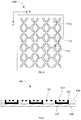
- the single-layer multi-point touch-control conductive film 100 includes a transparent substrate 110, a bridging module 120, a transparent polymer sub-layer 130 and a conductive module 140.
- the transparent substrate 110 has a first surface and a second surface opposite to the first surface.
- the shape of the transparent substrate 110 can be designed according to the shape of the single-layer multi-point touch-control conductive film 100, for example, the transparent substrate 110 can be rectangular.
- the bridging module 120 being made of a conductive material, is provided on the first surface of the transparent substrate 110.
- the bridging module 120 can be made of a metallic conductive material, and the transparent substrate 110 can be a transparent glass substrate in this state.
- the metallic conductive material may have a line shape with a line width range of 500 nm ⁇ 6 ⁇ m.
- the metallic conductive material can be a nontransparent metallic conductive material with a line width range of 500 nm ⁇ 6 ⁇ m, achieving a purpose of optical transparent and avoiding affecting a user's vision.
- the bridging module 120 also can be made of a transparent conductive material.
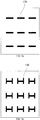
- the bridging module 120 can be a single line segment, or a structure formed by two line segments that are connected via at least one connecting line segment.
- the bridging module 120 illustrated in Fig. 3a is a single line segment
- the bridging module 120 illustrated in Fig. 3b is an H-shaped structure formed by two line segments being connected via one connecting line segment
- the bridging module 120 illustrated in Fig. 3c is a ⁇ -shaped structure formed by two line segments being connected via at two connecting line segments.
- the line segment forming the bridging module 120 has a width range of 1 ⁇ 6 ⁇ m.
- the transparent polymer sub-layer 130 is provided on the first surface of the transparent substrate 110, and covers the bridging module 120.
- the transparent polymer sub-layer 130 is formed with a first groove-shaped grid 131 on its surface, the first groove-shaped grid 131 is filled with a conductive material, respectively forming a first electrode 133 and a plurality of second electrode modules 135a.
- the first electrode 133 is arranged extending along a first dimension direction, and the plurality of second electrode modules 135a are arranged at spaced intervals along a second dimension direction intersecting with the first dimension direction.
- the bridging module 120 is configured to electrically connect two adjacent second electrode modules 135a, so as to form a column of second electrodes 135 extending along the second dimension direction.
- the transparent polymer sub-layer 130 can be UV glue, imprint glue or polycarbonate.
- the first electrode 133 can be a driving electrode, and the second electrode 135 can be a sensing electrode.
- the first dimension direction can be orthogonal, or inclined to the second dimension direction, particularly, in the illustrated embodiments, the first dimension direction is Y-axis and the second dimension direction is X-axis, constituting a rectangular coordinate system.
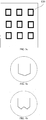
- the first groove-shaped grid 131 can have a V-shaped, W-shaped, curved, or corrugated microgroove at the bottom of the groove.
- the first groove-shaped grid 131 illustrated in Fig. 4a has a V-shaped microgroove at the bottom of the groove
- the first groove-shaped grid 131 illustrated in Fig. 4b has a W-shaped microgroove at the bottom of the groove
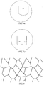
- the first groove-shaped grid 131 illustrated in Fig. 4c has a curved microgroove at the bottom of the groove
- the first groove-shaped grid 131 illustrated in Fig. 4d has a corrugated microgroove at the bottom of the groove.
- the microgroove has a depth range of 500 nm ⁇ 1 ⁇ m.
- the first groove-shaped grid 131 can have a V-shaped, W-shaped, curved, or corrugated microgroove at the bottom of the groove, during drying of the conductive ink filled in the groove of the first groove-shaped grid 131, the dried conductive ink material does not easily break when the conductive ink shrinks during the solidification thereof.
- the conductive module 140 is embedded in the transparent polymer sub-layer 130, and penetrating the transparent polymer sub-layer 130, so that the conductive module 140 can be in direct electrical connection with the bridging module 120.
- Each of the second electrode modules 135a is in electrical connection with the bridging module 120 via the conductive module 140, so as to form the second electrode 135.
- the conductive module 140 is provided on two ends of the line segment; when the bridging module 120 has a structure formed by two line segments being connected via at least one connecting line segment, the conductive module 140 is provided on the two line segments.
- the conductive module 140 is in a line segment shape with a width range of 500 nm ⁇ 5 ⁇ m.
- the conductive module 140 can be made of a transparent conductive material.
- the conductive module 140 and the bridging module 120 have transmittance of greater than 80%.
- the single-layer multi-point touch-control conductive film further includes a lead electrode, provided in a non-viewing area of the single-layer multi-point touchcontrol conductive film 100, and the conductive material of the lead electrode is in electrical connection with the conductive material in the first groove-shaped grid.
- the surface edge of the transparent polymer sub-layer 130 corresponding to the non-viewing area of the single-layer multi-point touch-control conductive film 100 is formed with a second groove-shaped grid being filled with a conductive material to form the lead electrode.
- the first groovelike grid and the second groove-shaped grid can be a regular grid or a random grid.
- the first groove-shaped grid and the second groove-shaped grid have a groove width of d1 and a depth of h, where 1 ⁇ m ⁇ d1 ⁇ 5 ⁇ m, 2 ⁇ m ⁇ h ⁇ 6 ⁇ m, h/d 1>1.
- the lead electrode is a grid-like or line-like conductive material formed on the transparent substrate 110 or provided on the surface edge of the transparent polymer sub-layer 130, and arranged corresponding to the non-viewing area of the single-layer multi-point touch-control conductive film 100.
- the single-layer multi-point touch-control conductive film 100 further includes a transparent protective sub-layer covering the transparent polymer sub-layer 130, and the transparent protective sub-layer can be UV glue, imprint glue or polycarbonate.
- all the conductive materials in this embodiment are preferable transparent conductive materials and, of course, nontransparent conductive materials also can be used in other embodiments.
- a single-layer multi-point touch-control conductive film 200 in a second embodiment is substantially the same as the single-layer multi-point touchcontrol conductive film 100 in the first embodiment, except for that: the single-layer multipoint touch-control conductive film 200 further includes a light shielding sub-layer 260, provided on the edge of the transparent substrate 110, for forming the non-viewing area.
- the light shielding sub-layer 260 can be made of ink or black resist.
- the above single-layer multi-point touch-control conductive film 100 has at least the following advantages:
- the present invention also provides a method for producing a single-layer multi-point touch-control conductive film, e.g., for producing the above single-layer multipoint touch-control conductive film 100.
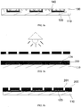
- the method for producing the single-layer multi-point touch control conductive film 100 in this embodiment includes steps S201 ⁇ S205:
- the step of forming the conductive module 140 on the bridging module 120 includes:
- Step S203 as shown in FIG. 8d , a layer of transparent polymer is applied on the first surface of the transparent substrate 110, with the transparent polymer embedding the conductive module 140, to form the transparent polymer sub-layer 130.
- the transparent polymer sub-layer 130 is provided on the first surface of the transparent substrate 110, and covers the bridging module 120.
- the transparent polymer sub-layer 130 is formed with a first groove-shaped grid 131 on its surface, the first groove-shaped grid 131 is filled with a conductive material, respectively forming a first electrode 133 and a plurality of second electrode modules 135a.
- the first electrode 133 is arranged extending along a first dimension direction, and the plurality of second electrode modules 135a are arranged at spaced intervals along a second dimension direction intersecting with the first dimension direction.
- the bridging module 120 is configured to electrically connect two adjacent second electrode modules 135a, so as to form a column of second electrodes 135 extending along the second dimension direction.
- the transparent polymer sub-layer 130 is formed with a first groove-shaped grid 131 on its surface.
- the transparent polymer sub-layer 130 can be UV glue, imprint glue or polycarbonate.
- the first groove-shaped grid 131 can have a V-shaped, W-shaped, curved, or corrugated microgroove at the bottom of the groove thereof.
- the first groove-shaped grid 131 can have a V-shaped, W-shaped, curved, or corrugated microgroove at the bottom of the groove.
- the microgroove has a depth range of 500 nm ⁇ 1 ⁇ m.
- the transparent polymer sub-layer 130 is imprint glue, and forms the first groove-shaped grid 131 by imprinting.
- Step S205 the first groove-shaped grid 131 is filled with a conductive material being in direct connection with the conductive module 140, to form the first electrode 133 and the second electrode 135.
- the first electrode 133 can be a driving electrode
- the second electrode 135 can be an sensing electrode.
- the method further includes a step of forming a light shielding sub-layer on the transparent substrate before, at or after step S202.
- the light shielding sub-layer can be formed on the transparent substrate by ink spraying and coating.
- the method further includes a step of forming a light shielding sub-layer on the transparent substrate.
Landscapes
- Engineering & Computer Science (AREA)
- General Engineering & Computer Science (AREA)
- Theoretical Computer Science (AREA)
- Human Computer Interaction (AREA)
- Physics & Mathematics (AREA)
- General Physics & Mathematics (AREA)
- Quality & Reliability (AREA)
- Position Input By Displaying (AREA)
- Laminated Bodies (AREA)
- Non-Insulated Conductors (AREA)
Claims (16)
- Film conducteur monocouche pour commande tactile multipoint (100) comprenant:un substrat transparent (110) comportant une première surface et une seconde surface opposée à la première surface;un module de raccordement (120) réalisé en un matériau conducteur et disposé sur la première surface du substrat transparent (110);une sous-couche polymère transparente (130) disposée sur la première surface du substrat transparent (110), en ce que la sous-couche polymère transparente (130) recouvre le module de raccordement (120); la sous-couche polymère transparente (130) est formée avec une première grille en forme de rainure (131) sur une surface de cette dernière, la première grille en forme de rainure (131) est remplie d'un matériau conducteur, formant respectivement une première électrode (133) et une pluralité de seconds modules d'électrode (135a), la première électrode (133) est disposée s'étendant le long d'une première direction de dimension, la pluralité de seconds modules d'électrode (135a) sont disposés à des intervalles espacés le long d'une seconde direction de dimension coupant la première direction de dimension, le module de raccordement (120) est configuré pour connecter électriquement deux seconds modules d'électrode adjacents (135a) de manière à former une colonne de secondes électrodes (135) s'étendant le long de la seconde direction de dimension; etun module conducteur (140) intégré dans la sous-couche polymère transparente (130) et pénétrant la sous-couche polymère transparente (130) de sorte que le module conducteur (140) soit en connexion électrique directe avec le module de raccordement (120); chacun des seconds modules d'électrode (135a) est une connexion électrique avec le module de raccordement (120) via le module conducteur (140) de manière à former la seconde électrode (135).
- Film conducteur monocouche pour commande tactile multipoint (100) selon la revendication 1, en ce que le module de raccordement (120) est réalisé en un matériau conducteur métallique en forme de ligne d'une largeur de ligne dans une plage comprise entre 500 nm et 6 µm.
- Film conducteur monocouche pour commande tactile multipoint (100) selon la revendication 1, en ce que le module de raccordement (120) comprend un segment de ligne ou une structure formée par deux segments de ligne connectés par l'intermédiaire d'au moins un segment de ligne de connexion.
- Film conducteur monocouche pour commande tactile multipoint (100) selon la revendication 3, en ce que le segment de ligne présente une largeur dans une plage comprise entre 1 et 6 µm.
- Film conducteur monocouche pour commande tactile multipoint (100) selon la revendication 3, en ce que, lorsque le module de raccordement (120) comprend le segment de ligne, le module conducteur (140) est ménagé sur les deux extrémités du segment de ligne; lorsque le module de raccordement (120) comprend la structure formée par deux segments de ligne connectés par l'intermédiaire d'au moins un segment de ligne de connexion, le module conducteur (140) est ménagé sur les deux segments de ligne.
- Film conducteur monocouche pour commande tactile multipoint (100) selon la revendication 5, en ce que le module conducteur (140) est en forme de segment de ligne d'une largeur dans une plage comprise entre 500 nm et 5 µm.
- Film conducteur monocouche pour commande tactile multipoint (100) selon la revendication 1, en ce que la première grille en forme de rainure (131) et la seconde grille en forme de rainure présentent une largeur de rainure de d1 et une profondeur de h, en ce que 1 µm ≤ d1 ≤ 5 µm, 2 µm ≤ h ≤ 6 µm, h/d1 > 1.
- Film conducteur monocouche pour commande tactile multipoint (100) selon la revendication 1, en ce que l'électrode au plomb est de type grille ou un matériau conducteur de type ligne formée sur le substrat transparent (110) ou ménagée sur le bord de la surface de la sous-couche polymère transparente (130) et disposée de manière à correspondre à la zone de non-visualisation du film conducteur monocouche pour commande tactile multipoint (100).
- Film conducteur monocouche pour commande tactile multipoint (100) selon la revendication 1, en ce que la première grille en forme de rainure (131) présente une forme en V, en W, est incurvée ou une micro-rainure ondulée sur la partie inférieure de la rainure.
- Film conducteur monocouche pour commande tactile multipoint (100) selon la revendication 9, en ce que la micro-rainure présente une largeur dans une plage comprise entre 500 nm et 1 µm.
- Procédé de production du film conducteur monocouche pour commande tactile multipoint selon l'une des revendications 1 à 10, comprenant:l'application d'un matériau conducteur sur la première surface du substrat transparent afin de former le module de raccordement (S201);la formation du module conducteur sur le module de raccordement (S202);l'application d'une couche de polymère transparent sur la première surface du substrat transparent, avec le module conducteur intégré dans le polymère transparent afin de former la sous-couche polymère transparente (S203);la formation de la première grille en forme de rainure sur la surface de la sous-couche polymère transparente (S204); etle remplissage de la première grille en forme de rainure avec un matériau conducteur étant en connexion directe avec le module conducteur afin de former la première électrode et la seconde électrode (S205).
- Procédé de production du film conducteur monocouche pour commande tactile multipoint selon la revendication 11, en ce que l'étape de formation du module conducteur sur le module de raccordement (S202) comprend:la formation d'une couche de sous-couche d'agent photorésistant sur la première surface du substrat transparent, avec la sous-couche d'agent photorésistant recouvrant le module de raccordement;la formation d'un trou, correspondant à la forme du module conducteur, sur le module de raccordement avec un procédé de développement de photolithographie;le remplissage du trou avec un matériau conducteur afin de former le module conducteur; et éliminant la sous-couche d'agent photorésistant.
- Procédé de production du film conducteur monocouche pour commande tactile multipoint selon la revendication 11, en ce que la sous-couche polymère transparente est une colle pour surimpression, et forme la première grille en forme de rainure par surimpression.
- Procédé de production du film conducteur monocouche pour commande tactile multipoint selon la revendication 11, en ce que le substrat transparent est un substrat en verre transparent, et le module de raccordement est réalisé en un matériau conducteur métallique et formé sur la première surface du substrat transparent par placage de métaux.
- Procédé de production du film conducteur monocouche pour commande tactile multipoint selon la revendication 11, en ce que le module de raccordement est réalisé en un matériau conducteur transparent et formé sur la première surface du substrat transparent par impression au jet d'encre.
- Film conducteur monocouche pour commande tactile multipoint (100) selon la revendication 1, en ce qu'il comprend en outre une sous-couche protectrice transparente recouvrant la sous-couche polymère transparente (130), en ce que la sous-couche protectrice transparente est une colle UV, colle pour surimpression ou polycarbonate.
Applications Claiming Priority (3)
| Application Number | Priority Date | Filing Date | Title |
|---|---|---|---|
| CN2013102104265A CN103294270A (zh) | 2013-05-30 | 2013-05-30 | 单层多点式触控导电膜及其制备方法 |
| CN2013102096165A CN103309506A (zh) | 2013-05-30 | 2013-05-30 | 单层多点式触控导电膜及其制备方法 |
| CN2013102100758A CN103294269A (zh) | 2013-05-30 | 2013-05-30 | 单层多点式触控导电膜及其制备方法 |
Publications (3)
| Publication Number | Publication Date |
|---|---|
| EP2808770A2 EP2808770A2 (fr) | 2014-12-03 |
| EP2808770A3 EP2808770A3 (fr) | 2014-12-24 |
| EP2808770B1 true EP2808770B1 (fr) | 2016-06-08 |
Family
ID=50884665
Family Applications (1)
| Application Number | Title | Priority Date | Filing Date |
|---|---|---|---|
| EP14166652.9A Not-in-force EP2808770B1 (fr) | 2013-05-30 | 2014-04-30 | Film conducteur monocouche pour commande tactile multipoint et son procédé de production |
Country Status (6)
| Country | Link |
|---|---|
| US (1) | US9640294B2 (fr) |
| EP (1) | EP2808770B1 (fr) |
| JP (1) | JP5846457B2 (fr) |
| KR (1) | KR101639255B1 (fr) |
| TW (1) | TWI562048B (fr) |
| WO (1) | WO2014190790A1 (fr) |
Families Citing this family (13)
| Publication number | Priority date | Publication date | Assignee | Title |
|---|---|---|---|---|
| CN105094395A (zh) * | 2014-05-04 | 2015-11-25 | 宸鸿科技(厦门)有限公司 | 触控装置 |
| CN104407729B (zh) * | 2014-10-14 | 2018-01-09 | 业成光电(深圳)有限公司 | 电子装置、触控屏、透明导电膜及透明导电膜的制备方法 |
| CN104376899B (zh) * | 2014-10-14 | 2017-01-11 | 业成光电(深圳)有限公司 | 电子装置、触控屏、透明导电膜及透明导电膜的制备方法 |
| US20170075473A1 (en) | 2015-09-15 | 2017-03-16 | Hyundai Motor Company | Touch input device and method for manufacturing the same |
| KR102543985B1 (ko) * | 2015-10-27 | 2023-06-14 | 삼성전자주식회사 | 전도막 및 이를 포함하는 전자 소자 |
| CN106547397B (zh) * | 2016-10-19 | 2022-03-22 | 苏州维业达触控科技有限公司 | 一种透明导电膜的制作方法、透明导电膜和触控屏 |
| CN108920008B (zh) * | 2018-07-23 | 2021-10-15 | 意力(广州)电子科技有限公司 | 显示设备、触控面板、触控传感器及其制造方法 |
| CN111370163B (zh) * | 2018-12-25 | 2021-09-14 | 昇印光电(昆山)股份有限公司 | 导电膜 |
| CN112558819A (zh) * | 2019-09-10 | 2021-03-26 | 南昌欧菲光科技有限公司 | 导电膜结构、制作方法和触控屏、电子设备 |
| CN113219741B (zh) * | 2021-04-20 | 2022-12-13 | 绵阳惠科光电科技有限公司 | 一种显示面板和显示装置 |
| CN113772963B (zh) * | 2021-09-13 | 2023-07-07 | 芜湖长信科技股份有限公司 | 一种双面线路触摸屏结构及其制备方法 |
| CN116072332B (zh) * | 2021-10-29 | 2025-10-10 | 北京京东方技术开发有限公司 | 导电网格的制备方法和薄膜传感器的制备方法 |
| JP2025066865A (ja) | 2023-10-12 | 2025-04-24 | レノボ・シンガポール・プライベート・リミテッド | 表示装置、電子機器、および表示装置の製造方法 |
Family Cites Families (25)
| Publication number | Priority date | Publication date | Assignee | Title |
|---|---|---|---|---|
| TWI361996B (en) * | 2008-03-21 | 2012-04-11 | Elan Microelectronics Corp | Touch panel device |
| CN101546242A (zh) * | 2008-03-26 | 2009-09-30 | 义隆电子股份有限公司 | 触控面板装置 |
| KR100988797B1 (ko) | 2008-09-12 | 2010-11-05 | 주식회사 모젬 | 초슬림 터치 스크린 겸용 윈도우 |
| KR101055049B1 (ko) * | 2009-01-19 | 2011-08-05 | 엘지이노텍 주식회사 | 입력장치 |
| JP5278759B2 (ja) * | 2009-05-28 | 2013-09-04 | 凸版印刷株式会社 | 静電容量型入力装置 |
| TWM379802U (en) * | 2009-10-28 | 2010-05-01 | Shenzhen Laibao Hi Tech Co Ltd | Layout structure of capacitive touch screen |
| US8653378B2 (en) | 2010-03-24 | 2014-02-18 | Li-Li Fan | Structure of bridging electrode |
| JP5520776B2 (ja) * | 2010-10-20 | 2014-06-11 | 信越ポリマー株式会社 | センサーシートおよびその製造方法 |
| KR101051448B1 (ko) * | 2010-10-26 | 2011-07-22 | 한국기계연구원 | 인쇄기반 금속 배선을 이용한 투명전극 제조 방법 및 그 투명전극 |
| KR101367569B1 (ko) * | 2010-12-29 | 2014-02-28 | 주식회사 엘지화학 | 터치 스크린 및 이의 제조방법 |
| TWI459253B (zh) * | 2011-01-25 | 2014-11-01 | Chunghwa Picture Tubes Ltd | 觸控面板 |
| US20120218028A1 (en) * | 2011-02-28 | 2012-08-30 | Tpk Touch Solutions Inc. | Capacitive touch panel, touch sensor structure and a method for manufacturing the capacitive touch panel |
| CN102222538B (zh) | 2011-03-11 | 2012-12-05 | 苏州纳格光电科技有限公司 | 图形化的柔性透明导电薄膜及其制法 |
| TWI452508B (zh) * | 2011-05-27 | 2014-09-11 | Novatek Microelectronics Corp | 電容式觸碰面板的佈局結構及其製作方法 |
| KR101118727B1 (ko) | 2011-05-31 | 2012-03-12 | 에스맥 (주) | 박막형 멀티 터치 스크린 패널 및 그 제조방법 |
| JP2013246723A (ja) * | 2012-05-28 | 2013-12-09 | Mitsubishi Paper Mills Ltd | 静電容量型タッチパネル用光透過性電極 |
| CN102799311B (zh) | 2012-07-13 | 2015-03-04 | 北京京东方光电科技有限公司 | 触摸屏、包含该触摸屏的电子设备及触摸屏的制造方法 |
| CN102903423B (zh) * | 2012-10-25 | 2015-05-13 | 南昌欧菲光科技有限公司 | 透明导电膜中的导电结构、透明导电膜及制作方法 |
| CN102930922B (zh) * | 2012-10-25 | 2015-07-08 | 南昌欧菲光科技有限公司 | 一种具有各向异性导电的透明导电膜 |
| CN103309506A (zh) * | 2013-05-30 | 2013-09-18 | 南昌欧菲光科技有限公司 | 单层多点式触控导电膜及其制备方法 |
| CN103294270A (zh) * | 2013-05-30 | 2013-09-11 | 南昌欧菲光科技有限公司 | 单层多点式触控导电膜及其制备方法 |
| CN203311374U (zh) * | 2013-05-30 | 2013-11-27 | 南昌欧菲光科技有限公司 | 单层多点式触控导电膜 |
| CN103294269A (zh) * | 2013-05-30 | 2013-09-11 | 南昌欧菲光科技有限公司 | 单层多点式触控导电膜及其制备方法 |
| CN203338280U (zh) * | 2013-05-30 | 2013-12-11 | 南昌欧菲光科技有限公司 | 单层多点式触控导电膜 |
| CN203338281U (zh) * | 2013-05-30 | 2013-12-11 | 南昌欧菲光科技有限公司 | 单层多点式触控导电膜 |
-
2014
- 2014-02-28 WO PCT/CN2014/072739 patent/WO2014190790A1/fr not_active Ceased
- 2014-04-29 US US14/265,313 patent/US9640294B2/en not_active Expired - Fee Related
- 2014-04-30 EP EP14166652.9A patent/EP2808770B1/fr not_active Not-in-force
- 2014-05-21 TW TW103117731A patent/TWI562048B/zh not_active IP Right Cessation
- 2014-05-28 KR KR1020140064715A patent/KR101639255B1/ko not_active Expired - Fee Related
- 2014-05-30 JP JP2014112504A patent/JP5846457B2/ja not_active Expired - Fee Related
Also Published As
| Publication number | Publication date |
|---|---|
| JP2014235751A (ja) | 2014-12-15 |
| TWI562048B (en) | 2016-12-11 |
| EP2808770A2 (fr) | 2014-12-03 |
| US20140356582A1 (en) | 2014-12-04 |
| JP5846457B2 (ja) | 2016-01-20 |
| KR101639255B1 (ko) | 2016-07-13 |
| WO2014190790A1 (fr) | 2014-12-04 |
| TW201445409A (zh) | 2014-12-01 |
| EP2808770A3 (fr) | 2014-12-24 |
| US9640294B2 (en) | 2017-05-02 |
| KR20140141498A (ko) | 2014-12-10 |
Similar Documents
| Publication | Publication Date | Title |
|---|---|---|
| US9640294B2 (en) | Single-layer multi-point touch-control conductive film | |
| US9448672B2 (en) | Touch panel structure and fabrication method for the same | |
| TWI489362B (zh) | 觸控感測結構及其形成方法 | |
| JP5897204B2 (ja) | 静電容量式透明導電膜及びその製造方法 | |
| KR200479733Y1 (ko) | 편광자 모듈, 그의 제조 방법 및 그를 이용한 터치 스크린 | |
| CN102654806A (zh) | 一种触控面板及其制造方法 | |
| CN105278786B (zh) | 触摸板 | |
| JP5798270B1 (ja) | タッチパネル | |
| TWI480783B (zh) | 觸控裝置及其形成方法 | |
| US9426885B2 (en) | Multi-layer micro-wire structure | |
| US20160041659A1 (en) | Touch panels and fabrication methods thereof | |
| KR101370443B1 (ko) | 터치패널의 전극 패턴 | |
| JP5520776B2 (ja) | センサーシートおよびその製造方法 | |
| US20150253901A1 (en) | Manufacturing method for single-sided multi-layer circuit pattern for touch panel | |
| CN203882639U (zh) | 导电膜及包含有该导电膜的触摸屏 | |
| CN103426504A (zh) | 导电膜 | |
| CN203149519U (zh) | 触控装置 | |
| US9296013B2 (en) | Making multi-layer micro-wire structure | |
| JP2012079169A (ja) | 検出基板およびその製造方法 | |
| CN203338280U (zh) | 单层多点式触控导电膜 | |
| CN103309506A (zh) | 单层多点式触控导电膜及其制备方法 | |
| TWI612448B (zh) | 觸控面板及其製造方法 | |
| CN203311374U (zh) | 单层多点式触控导电膜 | |
| CN203338281U (zh) | 单层多点式触控导电膜 | |
| CN103294269A (zh) | 单层多点式触控导电膜及其制备方法 |
Legal Events
| Date | Code | Title | Description |
|---|---|---|---|
| PUAL | Search report despatched |
Free format text: ORIGINAL CODE: 0009013 |
|
| PUAI | Public reference made under article 153(3) epc to a published international application that has entered the european phase |
Free format text: ORIGINAL CODE: 0009012 |
|
| 17P | Request for examination filed |
Effective date: 20140430 |
|
| AK | Designated contracting states |
Kind code of ref document: A2 Designated state(s): AL AT BE BG CH CY CZ DE DK EE ES FI FR GB GR HR HU IE IS IT LI LT LU LV MC MK MT NL NO PL PT RO RS SE SI SK SM TR |
|
| AX | Request for extension of the european patent |
Extension state: BA ME |
|
| RIC1 | Information provided on ipc code assigned before grant |
Ipc: G06F 3/044 20060101AFI20141113BHEP |
|
| AK | Designated contracting states |
Kind code of ref document: A3 Designated state(s): AL AT BE BG CH CY CZ DE DK EE ES FI FR GB GR HR HU IE IS IT LI LT LU LV MC MK MT NL NO PL PT RO RS SE SI SK SM TR |
|
| AX | Request for extension of the european patent |
Extension state: BA ME |
|
| RBV | Designated contracting states (corrected) |
Designated state(s): AL AT BE BG CH CY CZ DE DK EE ES FI FR GB GR HR HU IE IS IT LI LT LU LV MC MK MT NL NO PL PT RO RS SE SI SK SM TR |
|
| 17Q | First examination report despatched |
Effective date: 20150515 |
|
| GRAP | Despatch of communication of intention to grant a patent |
Free format text: ORIGINAL CODE: EPIDOSNIGR1 |
|
| INTG | Intention to grant announced |
Effective date: 20151123 |
|
| GRAS | Grant fee paid |
Free format text: ORIGINAL CODE: EPIDOSNIGR3 |
|
| GRAA | (expected) grant |
Free format text: ORIGINAL CODE: 0009210 |
|
| AK | Designated contracting states |
Kind code of ref document: B1 Designated state(s): AL AT BE BG CH CY CZ DE DK EE ES FI FR GB GR HR HU IE IS IT LI LT LU LV MC MK MT NL NO PL PT RO RS SE SI SK SM TR |
|
| REG | Reference to a national code |
Ref country code: GB Ref legal event code: FG4D |
|
| REG | Reference to a national code |
Ref country code: CH Ref legal event code: EP |
|
| REG | Reference to a national code |
Ref country code: IE Ref legal event code: FG4D |
|
| REG | Reference to a national code |
Ref country code: AT Ref legal event code: REF Ref document number: 805671 Country of ref document: AT Kind code of ref document: T Effective date: 20160715 |
|
| REG | Reference to a national code |
Ref country code: DE Ref legal event code: R096 Ref document number: 602014002231 Country of ref document: DE |
|
| REG | Reference to a national code |
Ref country code: LT Ref legal event code: MG4D |
|
| REG | Reference to a national code |
Ref country code: NL Ref legal event code: MP Effective date: 20160608 |
|
| PG25 | Lapsed in a contracting state [announced via postgrant information from national office to epo] |
Ref country code: FI Free format text: LAPSE BECAUSE OF FAILURE TO SUBMIT A TRANSLATION OF THE DESCRIPTION OR TO PAY THE FEE WITHIN THE PRESCRIBED TIME-LIMIT Effective date: 20160608 Ref country code: NO Free format text: LAPSE BECAUSE OF FAILURE TO SUBMIT A TRANSLATION OF THE DESCRIPTION OR TO PAY THE FEE WITHIN THE PRESCRIBED TIME-LIMIT Effective date: 20160908 Ref country code: LT Free format text: LAPSE BECAUSE OF FAILURE TO SUBMIT A TRANSLATION OF THE DESCRIPTION OR TO PAY THE FEE WITHIN THE PRESCRIBED TIME-LIMIT Effective date: 20160608 |
|
| REG | Reference to a national code |
Ref country code: AT Ref legal event code: MK05 Ref document number: 805671 Country of ref document: AT Kind code of ref document: T Effective date: 20160608 |
|
| PG25 | Lapsed in a contracting state [announced via postgrant information from national office to epo] |
Ref country code: SE Free format text: LAPSE BECAUSE OF FAILURE TO SUBMIT A TRANSLATION OF THE DESCRIPTION OR TO PAY THE FEE WITHIN THE PRESCRIBED TIME-LIMIT Effective date: 20160608 Ref country code: LV Free format text: LAPSE BECAUSE OF FAILURE TO SUBMIT A TRANSLATION OF THE DESCRIPTION OR TO PAY THE FEE WITHIN THE PRESCRIBED TIME-LIMIT Effective date: 20160608 Ref country code: ES Free format text: LAPSE BECAUSE OF FAILURE TO SUBMIT A TRANSLATION OF THE DESCRIPTION OR TO PAY THE FEE WITHIN THE PRESCRIBED TIME-LIMIT Effective date: 20160608 Ref country code: RS Free format text: LAPSE BECAUSE OF FAILURE TO SUBMIT A TRANSLATION OF THE DESCRIPTION OR TO PAY THE FEE WITHIN THE PRESCRIBED TIME-LIMIT Effective date: 20160608 Ref country code: GR Free format text: LAPSE BECAUSE OF FAILURE TO SUBMIT A TRANSLATION OF THE DESCRIPTION OR TO PAY THE FEE WITHIN THE PRESCRIBED TIME-LIMIT Effective date: 20160909 Ref country code: HR Free format text: LAPSE BECAUSE OF FAILURE TO SUBMIT A TRANSLATION OF THE DESCRIPTION OR TO PAY THE FEE WITHIN THE PRESCRIBED TIME-LIMIT Effective date: 20160608 Ref country code: NL Free format text: LAPSE BECAUSE OF FAILURE TO SUBMIT A TRANSLATION OF THE DESCRIPTION OR TO PAY THE FEE WITHIN THE PRESCRIBED TIME-LIMIT Effective date: 20160608 |
|
| PG25 | Lapsed in a contracting state [announced via postgrant information from national office to epo] |
Ref country code: SK Free format text: LAPSE BECAUSE OF FAILURE TO SUBMIT A TRANSLATION OF THE DESCRIPTION OR TO PAY THE FEE WITHIN THE PRESCRIBED TIME-LIMIT Effective date: 20160608 Ref country code: CZ Free format text: LAPSE BECAUSE OF FAILURE TO SUBMIT A TRANSLATION OF THE DESCRIPTION OR TO PAY THE FEE WITHIN THE PRESCRIBED TIME-LIMIT Effective date: 20160608 Ref country code: IT Free format text: LAPSE BECAUSE OF FAILURE TO SUBMIT A TRANSLATION OF THE DESCRIPTION OR TO PAY THE FEE WITHIN THE PRESCRIBED TIME-LIMIT Effective date: 20160608 Ref country code: RO Free format text: LAPSE BECAUSE OF FAILURE TO SUBMIT A TRANSLATION OF THE DESCRIPTION OR TO PAY THE FEE WITHIN THE PRESCRIBED TIME-LIMIT Effective date: 20160608 Ref country code: EE Free format text: LAPSE BECAUSE OF FAILURE TO SUBMIT A TRANSLATION OF THE DESCRIPTION OR TO PAY THE FEE WITHIN THE PRESCRIBED TIME-LIMIT Effective date: 20160608 Ref country code: IS Free format text: LAPSE BECAUSE OF FAILURE TO SUBMIT A TRANSLATION OF THE DESCRIPTION OR TO PAY THE FEE WITHIN THE PRESCRIBED TIME-LIMIT Effective date: 20161008 |
|
| PG25 | Lapsed in a contracting state [announced via postgrant information from national office to epo] |
Ref country code: AT Free format text: LAPSE BECAUSE OF FAILURE TO SUBMIT A TRANSLATION OF THE DESCRIPTION OR TO PAY THE FEE WITHIN THE PRESCRIBED TIME-LIMIT Effective date: 20160608 Ref country code: PT Free format text: LAPSE BECAUSE OF FAILURE TO SUBMIT A TRANSLATION OF THE DESCRIPTION OR TO PAY THE FEE WITHIN THE PRESCRIBED TIME-LIMIT Effective date: 20161010 Ref country code: BE Free format text: LAPSE BECAUSE OF FAILURE TO SUBMIT A TRANSLATION OF THE DESCRIPTION OR TO PAY THE FEE WITHIN THE PRESCRIBED TIME-LIMIT Effective date: 20160608 Ref country code: PL Free format text: LAPSE BECAUSE OF FAILURE TO SUBMIT A TRANSLATION OF THE DESCRIPTION OR TO PAY THE FEE WITHIN THE PRESCRIBED TIME-LIMIT Effective date: 20160608 Ref country code: SM Free format text: LAPSE BECAUSE OF FAILURE TO SUBMIT A TRANSLATION OF THE DESCRIPTION OR TO PAY THE FEE WITHIN THE PRESCRIBED TIME-LIMIT Effective date: 20160608 |
|
| REG | Reference to a national code |
Ref country code: DE Ref legal event code: R097 Ref document number: 602014002231 Country of ref document: DE |
|
| PLBE | No opposition filed within time limit |
Free format text: ORIGINAL CODE: 0009261 |
|
| STAA | Information on the status of an ep patent application or granted ep patent |
Free format text: STATUS: NO OPPOSITION FILED WITHIN TIME LIMIT |
|
| 26N | No opposition filed |
Effective date: 20170309 |
|
| PG25 | Lapsed in a contracting state [announced via postgrant information from national office to epo] |
Ref country code: DK Free format text: LAPSE BECAUSE OF FAILURE TO SUBMIT A TRANSLATION OF THE DESCRIPTION OR TO PAY THE FEE WITHIN THE PRESCRIBED TIME-LIMIT Effective date: 20160608 Ref country code: SI Free format text: LAPSE BECAUSE OF FAILURE TO SUBMIT A TRANSLATION OF THE DESCRIPTION OR TO PAY THE FEE WITHIN THE PRESCRIBED TIME-LIMIT Effective date: 20160608 |
|
| REG | Reference to a national code |
Ref country code: CH Ref legal event code: PL |
|
| REG | Reference to a national code |
Ref country code: IE Ref legal event code: MM4A |
|
| REG | Reference to a national code |
Ref country code: FR Ref legal event code: ST Effective date: 20171229 |
|
| PG25 | Lapsed in a contracting state [announced via postgrant information from national office to epo] |
Ref country code: MC Free format text: LAPSE BECAUSE OF FAILURE TO SUBMIT A TRANSLATION OF THE DESCRIPTION OR TO PAY THE FEE WITHIN THE PRESCRIBED TIME-LIMIT Effective date: 20160608 Ref country code: FR Free format text: LAPSE BECAUSE OF NON-PAYMENT OF DUE FEES Effective date: 20170502 |
|
| PG25 | Lapsed in a contracting state [announced via postgrant information from national office to epo] |
Ref country code: LI Free format text: LAPSE BECAUSE OF NON-PAYMENT OF DUE FEES Effective date: 20170430 Ref country code: CH Free format text: LAPSE BECAUSE OF NON-PAYMENT OF DUE FEES Effective date: 20170430 Ref country code: LU Free format text: LAPSE BECAUSE OF NON-PAYMENT OF DUE FEES Effective date: 20170430 |
|
| PG25 | Lapsed in a contracting state [announced via postgrant information from national office to epo] |
Ref country code: IE Free format text: LAPSE BECAUSE OF NON-PAYMENT OF DUE FEES Effective date: 20170430 |
|
| PGFP | Annual fee paid to national office [announced via postgrant information from national office to epo] |
Ref country code: DE Payment date: 20180409 Year of fee payment: 5 |
|
| PG25 | Lapsed in a contracting state [announced via postgrant information from national office to epo] |
Ref country code: MT Free format text: LAPSE BECAUSE OF NON-PAYMENT OF DUE FEES Effective date: 20170430 |
|
| PG25 | Lapsed in a contracting state [announced via postgrant information from national office to epo] |
Ref country code: AL Free format text: LAPSE BECAUSE OF FAILURE TO SUBMIT A TRANSLATION OF THE DESCRIPTION OR TO PAY THE FEE WITHIN THE PRESCRIBED TIME-LIMIT Effective date: 20160608 |
|
| PGFP | Annual fee paid to national office [announced via postgrant information from national office to epo] |
Ref country code: GB Payment date: 20180417 Year of fee payment: 5 |
|
| PG25 | Lapsed in a contracting state [announced via postgrant information from national office to epo] |
Ref country code: HU Free format text: LAPSE BECAUSE OF FAILURE TO SUBMIT A TRANSLATION OF THE DESCRIPTION OR TO PAY THE FEE WITHIN THE PRESCRIBED TIME-LIMIT; INVALID AB INITIO Effective date: 20140430 |
|
| PG25 | Lapsed in a contracting state [announced via postgrant information from national office to epo] |
Ref country code: BG Free format text: LAPSE BECAUSE OF FAILURE TO SUBMIT A TRANSLATION OF THE DESCRIPTION OR TO PAY THE FEE WITHIN THE PRESCRIBED TIME-LIMIT Effective date: 20160608 |
|
| PG25 | Lapsed in a contracting state [announced via postgrant information from national office to epo] |
Ref country code: CY Free format text: LAPSE BECAUSE OF FAILURE TO SUBMIT A TRANSLATION OF THE DESCRIPTION OR TO PAY THE FEE WITHIN THE PRESCRIBED TIME-LIMIT Effective date: 20160608 |
|
| REG | Reference to a national code |
Ref country code: DE Ref legal event code: R119 Ref document number: 602014002231 Country of ref document: DE |
|
| PG25 | Lapsed in a contracting state [announced via postgrant information from national office to epo] |
Ref country code: MK Free format text: LAPSE BECAUSE OF FAILURE TO SUBMIT A TRANSLATION OF THE DESCRIPTION OR TO PAY THE FEE WITHIN THE PRESCRIBED TIME-LIMIT Effective date: 20160608 |
|
| GBPC | Gb: european patent ceased through non-payment of renewal fee |
Effective date: 20190430 |
|
| PG25 | Lapsed in a contracting state [announced via postgrant information from national office to epo] |
Ref country code: DE Free format text: LAPSE BECAUSE OF NON-PAYMENT OF DUE FEES Effective date: 20191101 Ref country code: GB Free format text: LAPSE BECAUSE OF NON-PAYMENT OF DUE FEES Effective date: 20190430 |
|
| PG25 | Lapsed in a contracting state [announced via postgrant information from national office to epo] |
Ref country code: TR Free format text: LAPSE BECAUSE OF FAILURE TO SUBMIT A TRANSLATION OF THE DESCRIPTION OR TO PAY THE FEE WITHIN THE PRESCRIBED TIME-LIMIT Effective date: 20160608 |