EP2811376B1 - In-Zellen-Berührungstafel und Spannungsprüfungsverfahren dafür - Google Patents
In-Zellen-Berührungstafel und Spannungsprüfungsverfahren dafür Download PDFInfo
- Publication number
- EP2811376B1 EP2811376B1 EP14150147.8A EP14150147A EP2811376B1 EP 2811376 B1 EP2811376 B1 EP 2811376B1 EP 14150147 A EP14150147 A EP 14150147A EP 2811376 B1 EP2811376 B1 EP 2811376B1
- Authority
- EP
- European Patent Office
- Prior art keywords
- transient
- wires
- pins
- touch
- touch panel
- Prior art date
- Legal status (The legal status is an assumption and is not a legal conclusion. Google has not performed a legal analysis and makes no representation as to the accuracy of the status listed.)
- Active
Links
Images


Classifications
-
- G—PHYSICS
- G09—EDUCATION; CRYPTOGRAPHY; DISPLAY; ADVERTISING; SEALS
- G09G—ARRANGEMENTS OR CIRCUITS FOR CONTROL OF INDICATING DEVICES USING STATIC MEANS TO PRESENT VARIABLE INFORMATION
- G09G3/00—Control arrangements or circuits, of interest only in connection with visual indicators other than cathode-ray tubes
- G09G3/006—Electronic inspection or testing of displays and display drivers, e.g. of LED or LCD displays
-
- G—PHYSICS
- G06—COMPUTING OR CALCULATING; COUNTING
- G06F—ELECTRIC DIGITAL DATA PROCESSING
- G06F3/00—Input arrangements for transferring data to be processed into a form capable of being handled by the computer; Output arrangements for transferring data from processing unit to output unit, e.g. interface arrangements
- G06F3/01—Input arrangements or combined input and output arrangements for interaction between user and computer
- G06F3/03—Arrangements for converting the position or the displacement of a member into a coded form
- G06F3/041—Digitisers, e.g. for touch screens or touch pads, characterised by the transducing means
-
- G—PHYSICS
- G06—COMPUTING OR CALCULATING; COUNTING
- G06F—ELECTRIC DIGITAL DATA PROCESSING
- G06F3/00—Input arrangements for transferring data to be processed into a form capable of being handled by the computer; Output arrangements for transferring data from processing unit to output unit, e.g. interface arrangements
- G06F3/01—Input arrangements or combined input and output arrangements for interaction between user and computer
- G06F3/03—Arrangements for converting the position or the displacement of a member into a coded form
- G06F3/041—Digitisers, e.g. for touch screens or touch pads, characterised by the transducing means
- G06F3/0412—Digitisers structurally integrated in a display
-
- G—PHYSICS
- G06—COMPUTING OR CALCULATING; COUNTING
- G06F—ELECTRIC DIGITAL DATA PROCESSING
- G06F3/00—Input arrangements for transferring data to be processed into a form capable of being handled by the computer; Output arrangements for transferring data from processing unit to output unit, e.g. interface arrangements
- G06F3/01—Input arrangements or combined input and output arrangements for interaction between user and computer
- G06F3/03—Arrangements for converting the position or the displacement of a member into a coded form
- G06F3/041—Digitisers, e.g. for touch screens or touch pads, characterised by the transducing means
- G06F3/0416—Control or interface arrangements specially adapted for digitisers
- G06F3/04164—Connections between sensors and controllers, e.g. routing lines between electrodes and connection pads
Definitions
- the invention relates to the field of liquid crystal display, and particularly to an in-cell touch panel and a voltage testing method thereof.
- a tested flexible printed circuit (FPC) pre-bonding method is usually adopted to perform voltage testing.
- An in-cell touch panel 10 includes an array substrate 102.
- the array substrate 102 includes a display region 101, and multiple signal lines are formed on the array substrate 102.
- the signal line includes a transient lead 103 formed at the periphery of the display region and pins connected correspondingly with the transient lead 103.
- Figure 2 is an enlarged view of the pins of Figure 1 .
- the pins include touch pins 104 and display pins 105, which are respectively connected with corresponding transient leads 103.
- the transient lead 103 includes a metal electrode, an insulating layer formed on the metal electrode, and a second wire formed on the insulating layer by depositing material such as indium tin oxide (ITO).
- ITO indium tin oxide
- the second wire is electrically connected with the transient lead 103 via a second through-hole 106 in the insulating layer.
- the second through-hole 106 is located above the metal electrode.
- the touch pins 104 and the display pins 105 are arranged at intervals on the same level.
- each of the detection portions of the test board needs to correspond to each of the individual touch pins 104 one-to-one. Moreover, when the detection portion of the test board is pressed onto the touch pins 104, the detection portion should not contact with the display pins 105 around the touch pins 104, therefore, the alignment of the detection portion and the touch pin 104 is very difficult and a window for testing is very small.
- Reference US 2013/077034 discloses an LCD device and a method of manufacturing the same, in which a passivation layer and a pixel electrode are simultaneously formed by a single mask process using a half tone mask, and thus, manufacturing efficiency increases, and a defective contact due to loss of the pixel electrode can be prevented in a pad area.
- the LCD device includes a pad part including a pad area and a contact area.
- the LCD device includes a pixel pad formed in the pad area, a pixel bar formed in the contact area, and a bridge layer contacting the pixel pad with the pixel bar.
- the bridge layer is formed as a single layer or multi layers, and formed of one or more of a transparent conductive material and an opaque conductive material.
- Reference WO 2013/018592 discloses a sensor electrode provided between an insulating substrate and a counter electrode which is electrically connected to a grid-shaped metal bridge via an insulating layer.
- Reference US 2010/085320 discloses a display device including: a rectangular display panel; a first film-like printed circuit board including a first terminal portion, the first film-like printed circuit board extending from one side of the rectangular display panel in a direction; a rectangular touch panel provided so as to be opposed to the rectangular display panel; and a second film-like printed circuit board including a second terminal portion, the second film-like printed circuit board extending from one side of the rectangular touch panel in the direction, the one side of the rectangular touch panel corresponding to a side parallel with and adjacent to the one side of the rectangular display panel, the first terminal portion and the second terminal portion being provided so that a connecting direction of the first terminal portion is different from a connecting direction of the second terminal portion.
- the touch pins 104 are usually widened in the design stage.
- the size of the touch pins 104 is too small, even if they are widened, only a width in an order of several hundreds of microns can be achieved in consideration of size limitations such as the gap between the pin and the border of the screen.
- the width of the touch pin 104 is very small, which is typically about 80 ⁇ m; and the gap between the touch pins 104 is also small, which is typically about 40 ⁇ m.
- the display pin 105 has a different voltage resistance from the touch pin 104. Therefore, when testing the FPC, it is unable to test multiple adjacent touch pins at the same time.
- there is a need to strictly align with each touch pin 104 while pre-bonding the FPC which results in a difficult operation and a low testing accuracy.
- the existing testing fixture is cumbersome and is unable to be used widely.
- the application provides an in-cell touch panel to solve the problem in the prior art that it is difficult to align with the touch pins when testing.
- the in-cell touch panel includes: an array substrate; a plurality of signal lines arranged at one side of the array substrate, where the signal line includes a transient lead, and a display pin or a touch pin which is connected with the transient lead; an insulating layer covering the transient lead of each of the plurality of signal lines; and first wires formed on the insulating layer, wherein the touch pins are spaced by the display pins and the first wires are only electrically connected with the transient leads connected with the touch pins via first through-holes in the insulating layer.
- the transient lead includes at least two first through-holes according to the application.
- the transient leads corresponding to at least two touch pins are provided with the first wires according to the application.
- the first wires are electrically connected with some of the transient leads connected with the touch pins.
- the transient leads corresponding to the display pins are not provided with the first wires according to the application.
- the in-cell touch panel further includes a second wire formed above the display pin and the touch pin, the second wire being electrically connected with the display pin and the touch pin respectively via a second through-hole in the insulating layer on the display pin and a second through-hole in the insulating layer on the touch pin.
- transient leads corresponding to at least three adjacent touch pins are grouped into one test group, and the width of the first wires on the transient leads at the outermost ends of the test group is larger than the width of the first wires on the transient leads in the middle of the test group.
- the width of the first wire on the transient leads in the middle of the test group is 50nm to 300nm; the width of the first wires on the transient leads at the outermost ends of the test group is 180 ⁇ m to 220 ⁇ m.
- the first wires are made from anticorrosive conductive material.
- the material of the first wires is indium tin oxide.
- the application further provides a voltage testing method for the in-cell touch panel described above.
- the method includes: providing a plurality of first test boards, with the first test board including a first detection portion; and connecting the first detection portion cooperatively with a first wire on a transient lead, and applying a signal to the first wire to perform voltage testing.
- each of the first test boards includes a plurality of first detection portions.
- the method further includes: providing a second test board, with the second test board including a second detection portion; connecting the second detection portion cooperatively with a display pin, and applying a signal to the display pin.
- the method may further include: providing a second test board, with the second test board including a second detection portion; and the transient lead corresponding to the display pin being provided with the first wire; connecting the second detection portion cooperatively with the first wire provided on the transient lead corresponding to the display pin, and applying a signal to the first wire provided on the transient lead corresponding to the corresponding display pin.
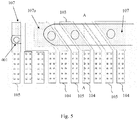
- Figure 3 is a top view of pins of an in-cell touch panel according to the present embodiment.
- the in-cell touch panel 10 of the present embodiment includes: an array substrate 102; multiple signal lines arranged at one side of the array substrate 102, with the signal line including a transient lead 103 and a display pin 105 and a touch pin 104 connected with the transient lead 103, and an insulating layer being attached on the transient lead 103.
- Some improvements are made to the transient leads 103 corresponding to the touch pins 104.
- Figure 6 is a cross-section view taken along A-A of Figure 3 .
- the transient leads 103 corresponding to a part of touch pins 104 are provided with first wires 107 thereon.
- the transient lead 103 includes a metal electrode 1031 formed by a photo-mask process and an insulating layer 1032 formed on the metal electrode 1031, where the insulating layer 1032 is used to protect the metal electrode 1031. Further, a first through-hole 1034 is etched in the insulating layer 1032 on the metal electrode 1031 by a photo-mask process, and the first wire 107 is deposited on the insulating layer 1032, with the first wire 107 being electrically connected with the metal electrode 1031 of the transient lead 103 via the first through-hole 1034.
- the material of the first wire 107 has an effect of electric conduction and anti-corrosion.
- the thickness of the insulating layer 1032 is 80nm, and the thickness of the first wire 107 is 100nm; the material of the first wire 107 is indium tin oxide (ITO).
- multiple first through-holes 1034 may be provided, so as to ensure that the electrical connection between the first wire 107 and the metal electrode 1031 can be achieved by other first through-holes 1034 in the case where a certain first through-hole 1034 does not expose the metal electrode 1031 due to incomplete etching of the insulating layer or in the case where the metal electrode 1031 is penetrated due to over-etching when forming a certain first through-hole 1034.
- the transient leads 103 provided with the first wires 107 are grouped into multiple test groups. Each test group includes the transient leads 103 corresponding to the adjacent multiple touch pins 104.
- the first wire 107 on the transient lead 103 at one outermost end of a same test group is widened, that is, this first wire 107 is wider than the first wires 107 on the transient leads 103 in the middle of the test group.
- the first wire 107 on the transient lead 103 at one outermost end of a same test group is widened, that is, this first wire 107 is wider than the first wires 107 on the transient leads 103 in the middle of the test group, therefore, it is convenient to identify the testing position with the naked eyes and thus achieve the accurate alignment of the test board when testing.
- the transient leads 103 corresponding to at least two touch pins 104 are provided with the first wires 107 thereon.
- the transient leads 103 corresponding to spaced touch pins 104 may be provided with the first wires 107 thereon.
- the touch pins 104 which are provided with the first wires 107 on their corresponding transient leads 103, it is possible to use a first test board 201 with multiple first detection portions 2011 to test multiple transient leads 103 provided with the first wires 107 at the same time; and for the remaining touch pins 104 which are not provided with the first wires 107 on their corresponding transient leads 103, the first test board 201 is directly connected cooperatively with these touch pins 104, then a signal is applied to perform voltage testing.
- the transient leads 103 corresponding to a part of touch pins 104 are provided with the first wires 107 thereon, a part of touch pins 104 to be tested can be transferred to the transient leads 103 corresponding to this part of touch pins 104, thus the number of the touch pins 104 on which the test is directly performed may be significantly reduced, which brings convenience to both of the practical detection operation and the design of the first test board 201.
- the first test board 201 is made from ITO coating film.
- the metal electrode of the transient lead 103 corresponding to the display pin 105 is provided with an insulating layer thereon, even if the area of the first test board 201 is increased, when the first test board 201 is pressed onto the transient leads 103 corresponding to the touch pins 104, some transient leads 103 corresponding to the display pins 105 may be pressed at the same time, the problem of short circuit between the pins can be avoided due to the presence of the insulating layer.
- a second test board 401 including a second detection portion is further needed to press any one of the display pins 105.
- both the contact region of each touch pin 104 with the detection portions of the test board and the contact region of each display pin 105 with the detection portions of the test board are formed from ITO conductive material.
- the electrical failures occurred in the testing for a touch panel may include an open circuit of a touch electrode, a weak connection of a touch electrode, a short circuit between touch electrodes and so on.
- the open circuit of the touch electrode and the short circuit of the touch electrode may be detected by monitoring the value of capacitance between the touch pin and the common electrode. If the value of the capacitance is too small, then the touch electrode may be open-circuited; and if the value of the capacitance is too large, then the touch electrode may be short-circuited.
- the weak connection of the touch electrode is mainly detected by detecting the magnitude of noise on a sensing electrode when a voltage is applied to a driving electrode.
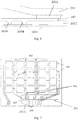
- FIG. 7 is a top view of the structure of the in-cell touch panel of the invention, which illustrates the specific voltage testing way for the touch pins.
- the transient leads 103 corresponding to the touch pins 104 are provided with the first wire 107 thereon. Since driving electrodes 301 and sensing electrodes 302 connected with each touch pins 104 have the same physical structure and the transient leads 103 corresponding to each touch pins 104 are close, these transient leads 103 provided with the first wires 107 may be grouped into multiple test groups.
- a first test board 201 is adopted to perform the test.
- the first test board 201 includes multiple test portions 2011, and the test portions 2011 of the first test board 201 are pressed onto the first wires on transient leads of the test groups to test the value of the capacitance. If there is one broken wire in the sensing electrodes (or the driving electrodes), as shown at B' in the figure, the measured capacitance value will be significantly small. If the measured capacitance value is significantly large, then a short circuit problem may exist between the driving electrode 301 and the sensing electrode 302, as shown at A' in the figure.
- the problem of weak connection may be determined by applying an electrical signal to the driving electrode 301 and reading the magnitude of noise on the signal received from the sensing electrode 302, and if the noise is large, then the measured current value fluctuates wildly and is unstable, thus the problem of weak connection exists.
- the in-cell touch panel 10 of the present embodiment includes: an array substrate 102; and multiple signal lines arranged at one side of the array substrate 102, with the signal line including a transient lead 103, and a display pin 105 and a touch pin 104 connected with the transient lead 103; and an insulating layer being attached on the transient lead 103.
- the transient leads 103 corresponding to all of the touch pins 104 are provided with the first wires 107 thereon.
- the transient lead 103 includes a metal electrode 1031 formed by a photo-mask process and an insulating layer 1032 formed on the metal electrode 1031, and the insulating layer 1032 is used to protect the metal electrode 1031.
- a first through-hole 1034 is etched in the insulating layer 1032 on the metal electrode 1031 with a photo-mask process, and the first wire 107 is deposited on the insulating layer 1032, with the first wire 107 being electrically connected with the metal electrode 1031 of the transient lead 103 via the first through-hole 1034.
- the material of the first wire 107 has an effect of electric conduction and anti-corrosion.
- the thickness of the insulating layer 1032 is 80nm, and the thickness of the first wire 107 is 100nm; the material of the first wire 107 is indium tin oxide (ITO).
- first through-holes 1034 may be provided, so as to ensure that the electrical connection between the first wire 107 and the metal electrode 1031 can be achieved by other first through-holes 1034 in the case where a certain first through-holes 1034 does not expose the metal electrode 1031 due to incomplete etching of the insulating layer or in the case where the metal electrode 1031 is penetrated due to over-etching when forming a certain first through-hole 1034.
- the transient leads 103 provided with the first wires 107 are grouped into multiple test groups. Each test group includes the transient leads 103 corresponding to multiple adjacent touch pins 104.
- the first wire 107 on the transient lead 103 at one outermost end of a same test group is widened, that is, the width of this first wire 107 is larger than that of the first wires 107 on the transient leads 103 in the middle of the test group.
- the first wire 107 on the transient lead 103 at one outermost end of a same test group is widened, that is, the width of this first wire 107 is larger than that of the first wires 107 on the transient leads 103 in the middle of the test group, therefore, it is convenient to identify the testing position with the naked eyes and thus the accurate alignment of the test board is achieved when testing.
- the structure of the second embodiment described above differs from the structure of the first embodiment in that the transient leads 103 corresponding to all of the touch pins 104 are provided with the first wires 107 thereon.
- the transient leads 103 corresponding to all of the touch pins 104 are pressed to perform the test; and the transient leads 103 corresponding the touch pins 104 are grouped into multiple test groups, each of the test groups includes multiple transient leads 103.
- a first test board 201 with multiple first detection portions 2011 is adopted to simultaneously press a group of transient leads to perform the test, so as to further reduce the difficulty in voltage testing for pins of the in-cell touch panel, and improve the testing accuracy significantly. Since there is no need to press the touch pins with smaller testing space, the difficulty in designing of the test board is reduced, and the testing convenience is improved.
- the first wire 107 on the transient lead 103 at one outermost end of a same test group is widened, that is, the width of this first wire 107 is larger than that of the first wires 107 on the transient leads 103 in the middle of the test group.
- the width of the first wire 107 on each transient leads 103 in the middle of the test groups is 50nm to 300nm; and for the transient lead at one outermost end of the test group, the width of the first wire 107 thereof is 180 ⁇ m to 220 ⁇ m.
- the in-cell touch panel 10 of the present embodiment includes: an array substrate 102; and multiple signal lines arranged at one side of the array substrate 102, with the signal line including a transient lead 103, a display pin 105 and a touch pin 104 connected with the transient lead 103; and an insulating layer being attached on the transient lead 103.
- the transient lead 103 includes a metal electrode 1031 formed by a photo-mask process and an insulating layer 1032 formed on the metal electrode 1031, and the insulating layer 1032 is used to protect the metal electrode 1031.
- a first through-hole 1034 is etched in the insulating layer 1032 on the metal electrode 1031 with a photo-mask process, and the first wire 107 is deposited on the insulating layer 1032, with the first wire 107 being electrically connected with the metal electrode 1031 of the transient lead 103 via the first through-hole 1034.
- the material of the first wire 107 has an effect of electric conduction and anti-corrosion.
- the thickness of the insulating layer 1032 is 80nm, and the thickness of the first wire 107 is 100nm; the material of the first wire 107 is indium tin oxide (ITO).
- first through-holes 1034 may be provided, so as to ensure that the electrical connection between the first wire 107 and the metal electrode 1031 can be achieved by other first through-holes 1034 in the case where a certain first through-holes 1034 does not expose the metal electrode 1031 due to incomplete etching of the insulating layer or in the case where the metal electrode 1031 is penetrated due to over-etching when forming a certain first through-hole 1034.
- the transient leads 103 provided with the first wires 107 are grouped into multiple test groups.
- Each test groups includes the transient leads 103 corresponding to multiple adjacent touch pins 104, in which the first wire 107 on the transient lead 103 at one outermost end of a same test group is widened, that is, the width of this first wire 107 is wider than that of the first wire 107s on the transient leads 103 in the middle of the test group.
- the first wires 107 on the transient lead 103 at two outermost ends of a same test group is widened, that is, these two first wires 107 are wider than the first wires 107 on the transient leads 103 in the middle of the test group, therefore, it is convenient to identify the testing position with the naked eyes and thus achieve the accurate alignment of the test board when testing.
- the structure of the third embodiment described above differs from the structure of the first embodiment in that the transient leads 103 corresponding to all of the touch pins 104 and the one display pin 105 are provided with the first wires 107, and the first wires 107 on the transient leads 103 at the two outermost ends of a same test group are widened.
- the transient leads 103 corresponding to all of the touch pins 104 are pressed to perform the test, and the transient lead 103 corresponding to the display pin 105 is also pressed at a corresponding voltage testing position, so as to further reduce the difficulty in voltage testing for pins of the in-cell touch panel, and improve the testing accuracy significantly. Since there is no need to press the touch pins and the display pins with smaller testing space, the difficulty in designing the test board is reduced, and the testing convenience is improved.
- the first wires 107 on the transient leads 103 at the outermost ends of each test group are widened, that is, the width of these first wires 107 is larger than that of the first wires 107 on the transient leads 103 in the middle of each test group, and is increased to for example 180 ⁇ m to 220 ⁇ m, so that it is easy to identify the position of each test group with the naked eyes and make the testing alignment more convenient.
- the arrangement manner that the first wire is provided on the transient lead corresponding to the touch pin and the arrangement manner that the first wire is provided on the transient lead corresponding to the display pin may be exchanged, that is, it is possible to provide the first wires on the transient leads corresponding to part or all the display pins, rather than on the transient leads corresponding to part or all the touch pins, to achieve the goal of testing the display pins simply.
- the in-cell touch panel of the invention can be applied to a touch panel structure using an In-Plane Switching (IPS) or Fringe Field Switching (FFS) mode.
- IPS In-Plane Switching
- FFS Fringe Field Switching
Landscapes
- Engineering & Computer Science (AREA)
- Theoretical Computer Science (AREA)
- General Engineering & Computer Science (AREA)
- Physics & Mathematics (AREA)
- General Physics & Mathematics (AREA)
- Human Computer Interaction (AREA)
- Computer Hardware Design (AREA)
- Computer Networks & Wireless Communication (AREA)
- Position Input By Displaying (AREA)
Claims (10)
- Zellenintegrierte berührungsempfindliche Tafel (10), Folgendes aufweisend:ein Anordnungssubstrat (102);mehrere Signalleitungen, die an einer Seite des Anordnungssubstrats angeordnet sind, wobei jede Signalleitung eine Übertragungsleitung (103) und einen Anzeige-Pin (105) oder Berührungs-Pin (104) aufweist, die mit der Übertragungsleitung verbunden sind;eine Isolierschicht (1032), die die Übertragungsleitung jeder der mehreren Signalleitungen bedeckt; underste Drähte (107), die auf der Isolierschicht gebildet sind,wobeidie Berührungs-Pins durch die Anzeige-Pins beabstandet sind und die ersten Drähte über erste Durchkontaktierungen (1034) in der Isolierschicht nur an die mit den Berührungs-Pins verbundenen Übertragungsleitungen elektrisch angeschlossen sind.
- Zellenintegrierte berührungsempfindliche Tafel nach Anspruch 1, wobei die Übertragungsleitung mindestens zwei erste Durchkontaktierungen aufweist.
- Zellenintegrierte berührungsempfindliche Tafel nach Anspruch 1 oder 2, wobei die Übertragungsleitungen, die mindestens zwei Berührungs-Pins entsprechen, mit den ersten Drähten verbunden sind.
- Zellenintegrierte berührungsempfindliche Tafel nach Anspruch 1, wobei die ersten Drähte mit einigen der Übertragungsleitungen elektrisch verbunden sind, die an die Berührungs-Pins angeschlossen sind.
- Zellenintegrierte berührungsempfindliche Tafel nach einem der vorhergehenden Ansprüche, wobei die den Anzeige-Pins entsprechenden Übertragungsleitungen nicht mit den ersten Drähten verbunden sind.
- Zellenintegrierte berührungsempfindliche Tafel nach einem der vorhergehenden Ansprüche, darüber hinaus aufweisend:zweite Drähte, die über dem Anzeige-Pin und Berührungs-Pin gebildet sind, wobei die zweiten Drähte über eine zweite Durchkontaktierung (106) in der Isolierschicht auf dem Anzeige-Pin und eine zweite Durchkontaktierung in der Isolierschicht auf dem Berührungs-Pin mit dem Anzeige-Pin bzw. Berührungs-Pin elektrisch verbunden sind.
- Zellenintegrierte berührungsempfindliche Tafel nach einem der vorhergehenden Ansprüche, wobei Übertragungsleitungen, die mindestens drei benachbarten Berührungs-Pins entsprechen, zu einer Prüfgruppe zusammengefasst sind, und die Breite der ersten Drähte auf den Übertragungsleitungen an den äußersten Enden der Prüfgruppe größer ist als die Breite der ersten Drähte auf den Übertragungsleitungen in der Mitte der Prüfgruppe.
- Zellenintegrierte berührungsempfindliche Tafel nach Anspruch 7, wobei die Breite der ersten Drähte auf den Übertragungsleitungen in der Mitte der Prüfgruppe 50nm bis 300nm beträgt; und die Breite der ersten Drähte auf den Übertragungsleitungen an den äußersten Enden der Prüfgruppe 180µm bis 220µm beträgt.
- Zellenintegrierte berührungsempfindliche Tafel nach einem der vorhergehenden Ansprüche, wobei die ersten Drähte aus einem korrosionsverhütenden leitfähigen Material bestehen.
- Zellenintegrierte berührungsempfindliche Tafel nach Anspruch 8 oder 9, wobei es sich bei dem Material der ersten Drähte um Indiumzinnoxid handelt.
Applications Claiming Priority (1)
| Application Number | Priority Date | Filing Date | Title |
|---|---|---|---|
| CN201310232233.XA CN103927038B (zh) | 2013-06-09 | 2013-06-09 | 一种内嵌式触摸屏及其电压检测方法 |
Publications (3)
| Publication Number | Publication Date |
|---|---|
| EP2811376A2 EP2811376A2 (de) | 2014-12-10 |
| EP2811376A3 EP2811376A3 (de) | 2015-04-15 |
| EP2811376B1 true EP2811376B1 (de) | 2017-11-08 |
Family
ID=50072850
Family Applications (1)
| Application Number | Title | Priority Date | Filing Date |
|---|---|---|---|
| EP14150147.8A Active EP2811376B1 (de) | 2013-06-09 | 2014-01-03 | In-Zellen-Berührungstafel und Spannungsprüfungsverfahren dafür |
Country Status (3)
| Country | Link |
|---|---|
| US (1) | US9666111B2 (de) |
| EP (1) | EP2811376B1 (de) |
| CN (1) | CN103927038B (de) |
Families Citing this family (10)
| Publication number | Priority date | Publication date | Assignee | Title |
|---|---|---|---|---|
| EP2985680B1 (de) * | 2014-08-14 | 2017-05-17 | LG Electronics Inc. | Leitfähige Folie, Berührungsbildschirm mit der leitfähigen Folie und Anzeigevorrichtung mit der leitfähigen Folie |
| CN104459400B (zh) * | 2014-12-08 | 2018-07-17 | 深圳市华星光电技术有限公司 | 用于自容式触摸屏的检测电路和检测方法 |
| KR102338753B1 (ko) * | 2015-04-14 | 2021-12-15 | 삼성디스플레이 주식회사 | 터치 패널 및 이를 포함하는 표시 장치 |
| US9910515B2 (en) * | 2016-04-27 | 2018-03-06 | Motorola Solutions, Inc. | User interface for a touchscreen of a portable communication device |
| CN106020545B (zh) * | 2016-05-20 | 2019-01-15 | 京东方科技集团股份有限公司 | 阵列基板及其制备方法、触摸屏 |
| CN108536324B (zh) * | 2017-03-03 | 2020-07-17 | 京东方科技集团股份有限公司 | 阵列基板及其制作方法、显示装置 |
| CN108628488B (zh) * | 2017-03-24 | 2021-06-29 | 南京瀚宇彩欣科技有限责任公司 | 内嵌式触控显示装置以及相关测试系统与测试方法 |
| CN108733242B (zh) * | 2017-04-17 | 2024-02-20 | 深圳莱宝高科技股份有限公司 | 金属引线触控面板及其制作方法 |
| CN108181541B (zh) * | 2018-01-29 | 2020-07-31 | 北京京东方光电科技有限公司 | 触控面板的检测装置及检测方法 |
| TWI767701B (zh) * | 2021-05-13 | 2022-06-11 | 友達光電股份有限公司 | 電路基板以及檢測方法 |
Family Cites Families (12)
| Publication number | Priority date | Publication date | Assignee | Title |
|---|---|---|---|---|
| US5060116A (en) * | 1990-04-20 | 1991-10-22 | Grobman Warren D | Electronics system with direct write engineering change capability |
| JP3525918B2 (ja) * | 2000-10-31 | 2004-05-10 | セイコーエプソン株式会社 | 電気光学装置、その検査方法および電子機器 |
| JP5106341B2 (ja) | 2008-10-02 | 2012-12-26 | 株式会社ジャパンディスプレイイースト | 表示装置 |
| KR101309862B1 (ko) * | 2009-12-10 | 2013-09-16 | 엘지디스플레이 주식회사 | 터치 패널 일체형 액정 표시 장치 |
| TWI441119B (zh) | 2010-04-02 | 2014-06-11 | Arolltech Co Ltd | 具內嵌觸控裝置之顯示器 |
| KR20120092365A (ko) | 2011-02-11 | 2012-08-21 | 삼성전자주식회사 | 정전용량방식 터치스크린패널 표시장치 |
| CN202177877U (zh) * | 2011-07-29 | 2012-03-28 | 比亚迪股份有限公司 | 电路板及具有其的触控装置 |
| WO2013018592A1 (ja) | 2011-07-29 | 2013-02-07 | シャープ株式会社 | タッチパネル基板および電気光学装置 |
| US9720295B2 (en) * | 2011-09-27 | 2017-08-01 | Lg Display Co., Ltd. | Liquid crystal display device and method for manufacturing the same |
| CN103105962B (zh) * | 2011-11-09 | 2016-04-06 | 宸鸿科技(厦门)有限公司 | 触控面板、触控电极结构及其制作方法 |
| CN102595774A (zh) | 2012-02-29 | 2012-07-18 | 博罗县精汇电子科技有限公司 | 便于测试的fpc高密度线路板及其测试方法 |
| TWI483361B (zh) * | 2012-03-23 | 2015-05-01 | 南茂科技股份有限公司 | 半導體封裝基板以及半導體封裝結構 |
-
2013
- 2013-06-09 CN CN201310232233.XA patent/CN103927038B/zh active Active
- 2013-12-19 US US14/135,509 patent/US9666111B2/en active Active
-
2014
- 2014-01-03 EP EP14150147.8A patent/EP2811376B1/de active Active
Non-Patent Citations (1)
| Title |
|---|
| None * |
Also Published As
| Publication number | Publication date |
|---|---|
| CN103927038A (zh) | 2014-07-16 |
| US9666111B2 (en) | 2017-05-30 |
| CN103927038B (zh) | 2017-08-29 |
| EP2811376A3 (de) | 2015-04-15 |
| US20140361786A1 (en) | 2014-12-11 |
| EP2811376A2 (de) | 2014-12-10 |
Similar Documents
| Publication | Publication Date | Title |
|---|---|---|
| EP2811376B1 (de) | In-Zellen-Berührungstafel und Spannungsprüfungsverfahren dafür | |
| CN105467632B (zh) | 一种液晶显示面板、其密封性检测方法及显示装置 | |
| US8653393B2 (en) | Touch screen panel | |
| US10180747B2 (en) | Touch display panel having touch electrodes and pressure sensing element and touch display device thereof | |
| JP5436485B2 (ja) | 入力装置 | |
| CN107015691B (zh) | 具有压力感测器的触控显示面板 | |
| US10248254B1 (en) | Display panel, display device and force touch method | |
| JP6188953B2 (ja) | 液晶ディスプレイ、液晶ディスプレイテスト方法及び電子装置 | |
| CN102955311B (zh) | 一种内置触控的液晶显示装置 | |
| US20100053114A1 (en) | Touch panel apparatus and method for manufacturing the same | |
| JP2013225266A (ja) | タッチパネル | |
| CN107704134A (zh) | 一种显示面板及显示装置 | |
| US10976591B2 (en) | Color filter substrate and method for preparing the same, and touch screen | |
| CN106932942B (zh) | 触控显示装置 | |
| US9811230B2 (en) | Touch panel and production method thereof | |
| WO2011026286A1 (zh) | 触控面板及触控面板的检测方法 | |
| CN111796713B (zh) | 显示面板 | |
| KR20170112464A (ko) | 터치 센서 및 이를 포함하는 화상 표시 장치 | |
| US9076604B2 (en) | Touch panel, a touch device, and a method for determining a location of a touch point | |
| KR102343598B1 (ko) | 터치 패널 및 이를 포함하는 화상 표시 장치 | |
| JP2013156949A (ja) | タッチパネル | |
| KR100322302B1 (ko) | 터치 패널의 전극 및 그 터치 패널이 부가된 평판디스플레이 | |
| TW201635120A (zh) | 觸控面板、觸控面板之檢查方法及觸控面板之製造方法 | |
| KR200253087Y1 (ko) | 터치 패널의 전극 구조 | |
| CN116434681A (zh) | 显示面板、电子设备及显示面板的测试方法 |
Legal Events
| Date | Code | Title | Description |
|---|---|---|---|
| PUAI | Public reference made under article 153(3) epc to a published international application that has entered the european phase |
Free format text: ORIGINAL CODE: 0009012 |
|
| 17P | Request for examination filed |
Effective date: 20140103 |
|
| AK | Designated contracting states |
Kind code of ref document: A2 Designated state(s): AL AT BE BG CH CY CZ DE DK EE ES FI FR GB GR HR HU IE IS IT LI LT LU LV MC MK MT NL NO PL PT RO RS SE SI SK SM TR |
|
| AX | Request for extension of the european patent |
Extension state: BA ME |
|
| PUAL | Search report despatched |
Free format text: ORIGINAL CODE: 0009013 |
|
| RIC1 | Information provided on ipc code assigned before grant |
Ipc: G06F 3/044 20060101ALI20150303BHEP Ipc: G01R 19/00 20060101ALI20150303BHEP Ipc: G06F 3/041 20060101AFI20150303BHEP Ipc: G09G 3/00 20060101ALI20150303BHEP |
|
| AK | Designated contracting states |
Kind code of ref document: A3 Designated state(s): AL AT BE BG CH CY CZ DE DK EE ES FI FR GB GR HR HU IE IS IT LI LT LU LV MC MK MT NL NO PL PT RO RS SE SI SK SM TR |
|
| AX | Request for extension of the european patent |
Extension state: BA ME |
|
| RAP1 | Party data changed (applicant data changed or rights of an application transferred) |
Owner name: SHANGHAI TIANMA MICRO-ELECTRONICS CO., LTD. Owner name: TIANMA MICRO-ELECTRONICS CO., LTD. |
|
| GRAP | Despatch of communication of intention to grant a patent |
Free format text: ORIGINAL CODE: EPIDOSNIGR1 |
|
| INTG | Intention to grant announced |
Effective date: 20170309 |
|
| GRAJ | Information related to disapproval of communication of intention to grant by the applicant or resumption of examination proceedings by the epo deleted |
Free format text: ORIGINAL CODE: EPIDOSDIGR1 |
|
| INTC | Intention to grant announced (deleted) | ||
| GRAP | Despatch of communication of intention to grant a patent |
Free format text: ORIGINAL CODE: EPIDOSNIGR1 |
|
| INTG | Intention to grant announced |
Effective date: 20170612 |
|
| GRAS | Grant fee paid |
Free format text: ORIGINAL CODE: EPIDOSNIGR3 |
|
| GRAA | (expected) grant |
Free format text: ORIGINAL CODE: 0009210 |
|
| AK | Designated contracting states |
Kind code of ref document: B1 Designated state(s): AL AT BE BG CH CY CZ DE DK EE ES FI FR GB GR HR HU IE IS IT LI LT LU LV MC MK MT NL NO PL PT RO RS SE SI SK SM TR |
|
| REG | Reference to a national code |
Ref country code: GB Ref legal event code: FG4D |
|
| REG | Reference to a national code |
Ref country code: CH Ref legal event code: EP Ref country code: AT Ref legal event code: REF Ref document number: 944758 Country of ref document: AT Kind code of ref document: T Effective date: 20171115 |
|
| REG | Reference to a national code |
Ref country code: IE Ref legal event code: FG4D |
|
| REG | Reference to a national code |
Ref country code: DE Ref legal event code: R096 Ref document number: 602014016786 Country of ref document: DE |
|
| REG | Reference to a national code |
Ref country code: NL Ref legal event code: MP Effective date: 20171108 |
|
| REG | Reference to a national code |
Ref country code: LT Ref legal event code: MG4D |
|
| REG | Reference to a national code |
Ref country code: AT Ref legal event code: MK05 Ref document number: 944758 Country of ref document: AT Kind code of ref document: T Effective date: 20171108 |
|
| PG25 | Lapsed in a contracting state [announced via postgrant information from national office to epo] |
Ref country code: LT Free format text: LAPSE BECAUSE OF FAILURE TO SUBMIT A TRANSLATION OF THE DESCRIPTION OR TO PAY THE FEE WITHIN THE PRESCRIBED TIME-LIMIT Effective date: 20171108 Ref country code: FI Free format text: LAPSE BECAUSE OF FAILURE TO SUBMIT A TRANSLATION OF THE DESCRIPTION OR TO PAY THE FEE WITHIN THE PRESCRIBED TIME-LIMIT Effective date: 20171108 Ref country code: NO Free format text: LAPSE BECAUSE OF FAILURE TO SUBMIT A TRANSLATION OF THE DESCRIPTION OR TO PAY THE FEE WITHIN THE PRESCRIBED TIME-LIMIT Effective date: 20180208 Ref country code: SE Free format text: LAPSE BECAUSE OF FAILURE TO SUBMIT A TRANSLATION OF THE DESCRIPTION OR TO PAY THE FEE WITHIN THE PRESCRIBED TIME-LIMIT Effective date: 20171108 Ref country code: NL Free format text: LAPSE BECAUSE OF FAILURE TO SUBMIT A TRANSLATION OF THE DESCRIPTION OR TO PAY THE FEE WITHIN THE PRESCRIBED TIME-LIMIT Effective date: 20171108 Ref country code: ES Free format text: LAPSE BECAUSE OF FAILURE TO SUBMIT A TRANSLATION OF THE DESCRIPTION OR TO PAY THE FEE WITHIN THE PRESCRIBED TIME-LIMIT Effective date: 20171108 |
|
| PG25 | Lapsed in a contracting state [announced via postgrant information from national office to epo] |
Ref country code: BG Free format text: LAPSE BECAUSE OF FAILURE TO SUBMIT A TRANSLATION OF THE DESCRIPTION OR TO PAY THE FEE WITHIN THE PRESCRIBED TIME-LIMIT Effective date: 20180208 Ref country code: IS Free format text: LAPSE BECAUSE OF FAILURE TO SUBMIT A TRANSLATION OF THE DESCRIPTION OR TO PAY THE FEE WITHIN THE PRESCRIBED TIME-LIMIT Effective date: 20180308 Ref country code: AT Free format text: LAPSE BECAUSE OF FAILURE TO SUBMIT A TRANSLATION OF THE DESCRIPTION OR TO PAY THE FEE WITHIN THE PRESCRIBED TIME-LIMIT Effective date: 20171108 Ref country code: HR Free format text: LAPSE BECAUSE OF FAILURE TO SUBMIT A TRANSLATION OF THE DESCRIPTION OR TO PAY THE FEE WITHIN THE PRESCRIBED TIME-LIMIT Effective date: 20171108 Ref country code: GR Free format text: LAPSE BECAUSE OF FAILURE TO SUBMIT A TRANSLATION OF THE DESCRIPTION OR TO PAY THE FEE WITHIN THE PRESCRIBED TIME-LIMIT Effective date: 20180209 Ref country code: RS Free format text: LAPSE BECAUSE OF FAILURE TO SUBMIT A TRANSLATION OF THE DESCRIPTION OR TO PAY THE FEE WITHIN THE PRESCRIBED TIME-LIMIT Effective date: 20171108 Ref country code: LV Free format text: LAPSE BECAUSE OF FAILURE TO SUBMIT A TRANSLATION OF THE DESCRIPTION OR TO PAY THE FEE WITHIN THE PRESCRIBED TIME-LIMIT Effective date: 20171108 |
|
| REG | Reference to a national code |
Ref country code: DE Ref legal event code: R082 Ref document number: 602014016786 Country of ref document: DE Representative=s name: EPPING HERMANN FISCHER PATENTANWALTSGESELLSCHA, DE Ref country code: DE Ref legal event code: R081 Ref document number: 602014016786 Country of ref document: DE Owner name: TIANMA MICRO-ELECTRONICS CO., LTD., CN Free format text: FORMER OWNER: TIANMA MICRO-ELECTRONICS CO., LTD., SHENZHEN, CN Ref country code: DE Ref legal event code: R081 Ref document number: 602014016786 Country of ref document: DE Owner name: SHANGHAI TIANMA MICRO-ELECTRONICS CO., LTD., CN Free format text: FORMER OWNER: TIANMA MICRO-ELECTRONICS CO., LTD., SHENZHEN, CN |
|
| PG25 | Lapsed in a contracting state [announced via postgrant information from national office to epo] |
Ref country code: SK Free format text: LAPSE BECAUSE OF FAILURE TO SUBMIT A TRANSLATION OF THE DESCRIPTION OR TO PAY THE FEE WITHIN THE PRESCRIBED TIME-LIMIT Effective date: 20171108 Ref country code: EE Free format text: LAPSE BECAUSE OF FAILURE TO SUBMIT A TRANSLATION OF THE DESCRIPTION OR TO PAY THE FEE WITHIN THE PRESCRIBED TIME-LIMIT Effective date: 20171108 Ref country code: DK Free format text: LAPSE BECAUSE OF FAILURE TO SUBMIT A TRANSLATION OF THE DESCRIPTION OR TO PAY THE FEE WITHIN THE PRESCRIBED TIME-LIMIT Effective date: 20171108 Ref country code: CY Free format text: LAPSE BECAUSE OF FAILURE TO SUBMIT A TRANSLATION OF THE DESCRIPTION OR TO PAY THE FEE WITHIN THE PRESCRIBED TIME-LIMIT Effective date: 20171108 Ref country code: CZ Free format text: LAPSE BECAUSE OF FAILURE TO SUBMIT A TRANSLATION OF THE DESCRIPTION OR TO PAY THE FEE WITHIN THE PRESCRIBED TIME-LIMIT Effective date: 20171108 |
|
| REG | Reference to a national code |
Ref country code: DE Ref legal event code: R097 Ref document number: 602014016786 Country of ref document: DE |
|
| PG25 | Lapsed in a contracting state [announced via postgrant information from national office to epo] |
Ref country code: PL Free format text: LAPSE BECAUSE OF FAILURE TO SUBMIT A TRANSLATION OF THE DESCRIPTION OR TO PAY THE FEE WITHIN THE PRESCRIBED TIME-LIMIT Effective date: 20171108 Ref country code: SM Free format text: LAPSE BECAUSE OF FAILURE TO SUBMIT A TRANSLATION OF THE DESCRIPTION OR TO PAY THE FEE WITHIN THE PRESCRIBED TIME-LIMIT Effective date: 20171108 Ref country code: IT Free format text: LAPSE BECAUSE OF FAILURE TO SUBMIT A TRANSLATION OF THE DESCRIPTION OR TO PAY THE FEE WITHIN THE PRESCRIBED TIME-LIMIT Effective date: 20171108 Ref country code: RO Free format text: LAPSE BECAUSE OF FAILURE TO SUBMIT A TRANSLATION OF THE DESCRIPTION OR TO PAY THE FEE WITHIN THE PRESCRIBED TIME-LIMIT Effective date: 20171108 |
|
| REG | Reference to a national code |
Ref country code: CH Ref legal event code: PL |
|
| PLBE | No opposition filed within time limit |
Free format text: ORIGINAL CODE: 0009261 |
|
| STAA | Information on the status of an ep patent application or granted ep patent |
Free format text: STATUS: NO OPPOSITION FILED WITHIN TIME LIMIT |
|
| 26N | No opposition filed |
Effective date: 20180809 |
|
| GBPC | Gb: european patent ceased through non-payment of renewal fee |
Effective date: 20180208 |
|
| PG25 | Lapsed in a contracting state [announced via postgrant information from national office to epo] |
Ref country code: LU Free format text: LAPSE BECAUSE OF NON-PAYMENT OF DUE FEES Effective date: 20180103 Ref country code: FR Free format text: LAPSE BECAUSE OF NON-PAYMENT OF DUE FEES Effective date: 20180131 |
|
| REG | Reference to a national code |
Ref country code: IE Ref legal event code: MM4A |
|
| REG | Reference to a national code |
Ref country code: FR Ref legal event code: ST Effective date: 20180928 |
|
| REG | Reference to a national code |
Ref country code: BE Ref legal event code: MM Effective date: 20180131 |
|
| PG25 | Lapsed in a contracting state [announced via postgrant information from national office to epo] |
Ref country code: SI Free format text: LAPSE BECAUSE OF FAILURE TO SUBMIT A TRANSLATION OF THE DESCRIPTION OR TO PAY THE FEE WITHIN THE PRESCRIBED TIME-LIMIT Effective date: 20171108 Ref country code: LI Free format text: LAPSE BECAUSE OF NON-PAYMENT OF DUE FEES Effective date: 20180131 Ref country code: CH Free format text: LAPSE BECAUSE OF NON-PAYMENT OF DUE FEES Effective date: 20180131 Ref country code: BE Free format text: LAPSE BECAUSE OF NON-PAYMENT OF DUE FEES Effective date: 20180131 |
|
| PG25 | Lapsed in a contracting state [announced via postgrant information from national office to epo] |
Ref country code: IE Free format text: LAPSE BECAUSE OF NON-PAYMENT OF DUE FEES Effective date: 20180103 |
|
| PG25 | Lapsed in a contracting state [announced via postgrant information from national office to epo] |
Ref country code: GB Free format text: LAPSE BECAUSE OF NON-PAYMENT OF DUE FEES Effective date: 20180208 |
|
| PG25 | Lapsed in a contracting state [announced via postgrant information from national office to epo] |
Ref country code: MC Free format text: LAPSE BECAUSE OF FAILURE TO SUBMIT A TRANSLATION OF THE DESCRIPTION OR TO PAY THE FEE WITHIN THE PRESCRIBED TIME-LIMIT Effective date: 20171108 |
|
| PG25 | Lapsed in a contracting state [announced via postgrant information from national office to epo] |
Ref country code: MT Free format text: LAPSE BECAUSE OF NON-PAYMENT OF DUE FEES Effective date: 20180103 |
|
| PG25 | Lapsed in a contracting state [announced via postgrant information from national office to epo] |
Ref country code: TR Free format text: LAPSE BECAUSE OF FAILURE TO SUBMIT A TRANSLATION OF THE DESCRIPTION OR TO PAY THE FEE WITHIN THE PRESCRIBED TIME-LIMIT Effective date: 20171108 |
|
| PG25 | Lapsed in a contracting state [announced via postgrant information from national office to epo] |
Ref country code: PT Free format text: LAPSE BECAUSE OF FAILURE TO SUBMIT A TRANSLATION OF THE DESCRIPTION OR TO PAY THE FEE WITHIN THE PRESCRIBED TIME-LIMIT Effective date: 20171108 Ref country code: HU Free format text: LAPSE BECAUSE OF FAILURE TO SUBMIT A TRANSLATION OF THE DESCRIPTION OR TO PAY THE FEE WITHIN THE PRESCRIBED TIME-LIMIT; INVALID AB INITIO Effective date: 20140103 |
|
| PG25 | Lapsed in a contracting state [announced via postgrant information from national office to epo] |
Ref country code: MK Free format text: LAPSE BECAUSE OF NON-PAYMENT OF DUE FEES Effective date: 20171108 |
|
| PG25 | Lapsed in a contracting state [announced via postgrant information from national office to epo] |
Ref country code: AL Free format text: LAPSE BECAUSE OF FAILURE TO SUBMIT A TRANSLATION OF THE DESCRIPTION OR TO PAY THE FEE WITHIN THE PRESCRIBED TIME-LIMIT Effective date: 20171108 |
|
| PGFP | Annual fee paid to national office [announced via postgrant information from national office to epo] |
Ref country code: DE Payment date: 20260120 Year of fee payment: 13 |