EP2811633A2 - Système et procédé de réduction de courant réactif sur un bus CC commun à plusieurs onduleurs - Google Patents
Système et procédé de réduction de courant réactif sur un bus CC commun à plusieurs onduleurs Download PDFInfo
- Publication number
- EP2811633A2 EP2811633A2 EP20140171100 EP14171100A EP2811633A2 EP 2811633 A2 EP2811633 A2 EP 2811633A2 EP 20140171100 EP20140171100 EP 20140171100 EP 14171100 A EP14171100 A EP 14171100A EP 2811633 A2 EP2811633 A2 EP 2811633A2
- Authority
- EP
- European Patent Office
- Prior art keywords
- inverter
- bus
- phase angle
- carrier phase
- voltage
- Prior art date
- Legal status (The legal status is an assumption and is not a legal conclusion. Google has not performed a legal analysis and makes no representation as to the accuracy of the status listed.)
- Granted
Links
Images





Classifications
-
- H—ELECTRICITY
- H02—GENERATION; CONVERSION OR DISTRIBUTION OF ELECTRIC POWER
- H02M—APPARATUS FOR CONVERSION BETWEEN AC AND AC, BETWEEN AC AND DC, OR BETWEEN DC AND DC, AND FOR USE WITH MAINS OR SIMILAR POWER SUPPLY SYSTEMS; CONVERSION OF DC OR AC INPUT POWER INTO SURGE OUTPUT POWER; CONTROL OR REGULATION THEREOF
- H02M1/00—Details of apparatus for conversion
- H02M1/14—Arrangements for reducing ripples from DC input or output
-
- H—ELECTRICITY
- H02—GENERATION; CONVERSION OR DISTRIBUTION OF ELECTRIC POWER
- H02J—ELECTRIC POWER NETWORKS; CIRCUIT ARRANGEMENTS OR SYSTEMS FOR SUPPLYING OR DISTRIBUTING ELECTRIC POWER; SYSTEMS FOR STORING ELECTRIC ENERGY
- H02J1/00—Circuit arrangements for DC mains or DC distribution networks
- H02J1/06—Two-wire DC power distribution systems
-
- H—ELECTRICITY
- H02—GENERATION; CONVERSION OR DISTRIBUTION OF ELECTRIC POWER
- H02M—APPARATUS FOR CONVERSION BETWEEN AC AND AC, BETWEEN AC AND DC, OR BETWEEN DC AND DC, AND FOR USE WITH MAINS OR SIMILAR POWER SUPPLY SYSTEMS; CONVERSION OF DC OR AC INPUT POWER INTO SURGE OUTPUT POWER; CONTROL OR REGULATION THEREOF
- H02M7/00—Conversion of AC power input into DC power output; Conversion of DC power input into AC power output
- H02M7/42—Conversion of DC power input into AC power output without possibility of reversal
- H02M7/44—Conversion of DC power input into AC power output without possibility of reversal by static converters
- H02M7/48—Conversion of DC power input into AC power output without possibility of reversal by static converters using discharge tubes with control electrode or semiconductor devices with control electrode
- H02M7/493—Conversion of DC power input into AC power output without possibility of reversal by static converters using discharge tubes with control electrode or semiconductor devices with control electrode the static converters being arranged for operation in parallel
-
- H—ELECTRICITY
- H02—GENERATION; CONVERSION OR DISTRIBUTION OF ELECTRIC POWER
- H02M—APPARATUS FOR CONVERSION BETWEEN AC AND AC, BETWEEN AC AND DC, OR BETWEEN DC AND DC, AND FOR USE WITH MAINS OR SIMILAR POWER SUPPLY SYSTEMS; CONVERSION OF DC OR AC INPUT POWER INTO SURGE OUTPUT POWER; CONTROL OR REGULATION THEREOF
- H02M1/00—Details of apparatus for conversion
- H02M1/0043—Converters switched with a phase shift, i.e. interleaved
-
- H—ELECTRICITY
- H02—GENERATION; CONVERSION OR DISTRIBUTION OF ELECTRIC POWER
- H02M—APPARATUS FOR CONVERSION BETWEEN AC AND AC, BETWEEN AC AND DC, OR BETWEEN DC AND DC, AND FOR USE WITH MAINS OR SIMILAR POWER SUPPLY SYSTEMS; CONVERSION OF DC OR AC INPUT POWER INTO SURGE OUTPUT POWER; CONTROL OR REGULATION THEREOF
- H02M1/00—Details of apparatus for conversion
- H02M1/0067—Converter structures employing plural converter units, other than for parallel operation of the units on a single load
- H02M1/008—Plural converter units for generating at two or more independent and non-parallel outputs, e.g. systems with plural point of load switching regulators
Definitions
- the subject matter disclosed herein relates generally to a system having a direct current (DC) bus which is shared by multiple inverters and, more specifically, to a system for reducing the amplitude of reactive current present on the DC bus as a result of the multiple inverters.
- DC direct current
- a motor drive receives an input voltage and converts the input voltage to a suitable output voltage for controlling operation of a motor.
- AC Alternating Current
- the motor drive includes a converter section that rectifies the AC input voltage into a Direct Current (DC) voltage.
- DC Direct Current
- the DC voltage is present across a first rail and a second rail of a DC bus in the motor drive.
- An inverter section includes switches, such as transistors, thyristors, or siliconcontrolled rectifiers to convert the DC voltage on the DC bus into an AC voltage output at the desired magnitude and frequency to control operation of the motor.
- the converter, DC bus, and inverter sections may be enclosed in a single housing as a centralized motor drive configured to be mounted in a control cabinet.
- a portion of the motor drive, such as the inverter section may be included in a separate housing or integrated into the motor housing and located by the motor to be controlled.
- the converter section may be included a housing configured to be mounted in the control cabinet.
- a DC link including a DC bus cable, as well as, inductive or capacitive elements connects the converter section to one or more distributed inverter sections.
- the motor drive often utilizes a pulse-width modulation (PWM) routine to control the switches in the inverter section.
- PWM pulse-width modulation
- the switches alternately connect and disconnect either the first or second rail of the DC bus to the AC output.
- the resulting output is, therefore, either zero volts or fully on at the voltage level present on the DC bus.
- the PWM routine In order to vary the magnitude of the output voltage, the PWM routine repeatedly executes at a predetermined interval, sometimes referred to as a carrier period, where the inverse of the carrier period is the carrier frequency.
- the PWM routine receives a reference signal corresponding to the desired output voltage magnitude and controls the switches such that the DC bus is connected to the output for a portion of the carrier period.
- the output is on for a percentage of the carrier period and off for the remaining percentage of the carrier period and an average voltage magnitude for each carrier period results.
- the average voltage magnitude varies such that it corresponds to the reference signal input to the PWM routine. If the fundamental frequency of the desired AC voltage is much less than the carrier frequency, the resulting output voltage waveform approximates the desired AC voltage.
- the high frequency switching generates undesirable reactive currents at the carrier frequency and harmonics, or multiples, thereof, which may be present, for example, on the DC bus.
- the reactive current present on the DC bus is of particular concern in a distributed motor drive.
- the inverter sections may be a significant distance from the converter section, and the DC bus cable and other reactive DC link components such as inductors and capacitors present a significant impedance to the high frequency reactive currents.
- the reactive currents are dissipated, at least in part, as power losses in the DC link components as a result of these impedances.
- each inverter sections are connected to a single converter, each generates reactive currents which are transferred to the DC bus, increasing the potential maximum amplitude of the reactive currents.
- the subject matter disclosed herein describes a system configured to reduce the amplitude of reactive current present on a DC bus shared by multiple inverters.
- the system may include one processor configured to control multiple inverters or multiple processors each configured to control a respective inverter.
- a synchronizing signal is generated by one of the processors to coordinate the start of each switching period for the modulation routines of each inverter.
- a carrier phase angle is determined for each of the inverters which defines the point within a carrier signal used by the modulation routine of each inverter that corresponds to the start of the switching period.
- the modulation routine of each inverter generates a reactive current, one component of which is known as a ripple current, on the shared DC bus.
- the reactive current of a first inverter may be generated at a phase angle that is offset from the phase angle of the reactive current generated by a second inverter.
- the reactive current from the first inverter cancels at least a portion of the reactive current from the second inverter, reducing the total reactive current present on the DC bus.
- a system for reducing a reactive current present on a DC bus has a first voltage rail and a second voltage rail and is configured to have a DC voltage potential present between the first voltage rail and the second voltage rail.
- the system includes a plurality of inverters, and each inverter includes an input configured to connect to the first and second voltage rails of the DC bus, an output configured to connect to an alternating current (AC) load, and a plurality of switching devices. Each switching device is controlled by a switching signal to alternately connect and disconnect the input to the output.
- AC alternating current
- a modulation module is configured to execute at a periodic interval. During each periodic interval the modulation module determines each of the switching signals as a function of a carrier signal that repeats within the periodic interval and at least one voltage reference signal. Each carrier signal is defined at least in part by a carrier phase angle, and each voltage reference signal corresponds to a desired output voltage for each phase of the AC load.
- a synchronizing signal is in communication with each of the modulation modules and is used by each modulation module to start its corresponding periodic interval at substantially the same time.
- a controller generates the carrier phase angle for each inverter.
- the carrier phase angle for each inverter is determined such that a first reactive current generated by the plurality of switching devices which alternately connect and disconnect the input to the output in a first inverter is at least partially cancelled by a second reactive current generated by the plurality of switching devices which alternately connect and disconnect the input to the output in a second inverter.
- an inverter for connection to a common DC bus has a first voltage rail, a second voltage rail, a DC voltage potential present between the first voltage rail and the second voltage rail, and at least one additional inverter connected to the common DC bus.
- the inverter includes a first input configured to receive a synchronizing signal, a second input configured to receive an indication of the number of additional inverters connected to the common DC bus, a DC bus input configured to connect to the first and second voltage rails of the common DC bus, an output configured to connect to an AC load, a memory device configured to store an identifier corresponding to each inverter, a controller configured to generate a carrier phase angle, and a plurality of switching devices controlled by a switching signal to alternately connect and disconnect the DC bus input to the output.
- the carrier phase angle is determined as a function of the number of additional inverters connected to the common DC bus and of the identifier.
- a modulation module is configured to execute at a periodic interval.
- a start time of each periodic interval is defined, at least in part, by the synchronizing signal, and during each periodic interval, the modulation module determines each of the switching signals as a function of a carrier signal that repeats within the periodic interval and at least one voltage reference signal.
- Each carrier signal is defined at least in part by the carrier phase angle and corresponds to a desired output voltage for each phase of the AC load.
- a method of controlling a plurality of inverters, where each inverter converts a DC voltage from a shared DC bus to an AC voltage is disclosed.
- a synchronizing signal is generated with a controller, and the synchronizing signal defines a start of a periodic interval for a modulation routine for each of the inverters.
- a carrier phase angle is determined for each of the inverters with the controller such that a first reactive current generated by a first inverter is at least partially cancelled by a second reactive current generated by a second inverter.
- a carrier signal is generated for the modulation routine for each of the inverters with the controller as a function of the carrier phase angle.
- the modulation module is executing for each inverter to determine a plurality of switching signals as a function of the carrier signal and of at least one voltage reference signal.
- Each voltage reference signal corresponds to a desired output voltage for each phase of the AC voltage and each switching signal controls a switching device to alternately connect and disconnect the DC bus to an output of the inverter.
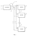
- a converter 11 receives power in a first form and provides it to the DC bus 13.
- the input may be a DC voltage or an AC voltage, where the AC voltage is either single phase or multi-phase.
- the converter 11 is configured to supply a regulated DC voltage on the DC bus 13.
- the system includes at least a first inverter 15 and a second inverter 15, but may include any number of additional inverters 15.
- Each inverter 15 converts the DC voltage present on the DC bus 13 to an AC voltage for use by an electrical load.
- Communication media 17 extends between the converter 11 and each inverter 15.
- the communication media 17 may be a single electrical conductor, multiple electrical conductors, a network cable configured to transmit data packets, or any other suitable communication media 17 configured to transmit data between the devices according to application requirements.
- the communication media 17 may extend only between the inverters 15.
- one embodiment of the present invention includes a motor drive 9 connected to a three phase AC input voltage 12.
- the motor drive 9 is configured with multiple inverter sections 32 and 42 to provide multiple outputs 14 and 18, respectively.
- the motor drive 9 generates a first output 14, illustrated as a three phase AC output voltage, to control a first motor 16, and a second output 18, also illustrated as a three phase AC output voltage, to control a second motor 20.
- the output voltage, 14 or 18, could be a single phase AC output voltage, a multi-phase AC output voltage, or a DC voltage, as required by the motor connected to the drive without deviating from the scope of the invention.
- the AC input voltage 12 is converted to a DC voltage present on the DC bus 24 by a converter section 22.
- the DC voltage potential is present between a first rail 28 and a second rail 30 of the DC bus 24.
- a DC bus capacitor 26 is connected between the first and second rails, 28 and 30, to reduce the magnitude of the reactive voltage resulting from converting the AC voltage to a DC voltage.
- the DC bus capacitor 26 may be a single capacitor or multiple capacitors connected in parallel, in series, or a combination thereof.
- the magnitude of the voltage potential between the first and second rails, 28 and 30, is generally about equal to or greater than the magnitude of the peak of the AC input voltage.
- the DC bus may include more than two rails including, but not limited to multiple positive rails, multiple negative rails, a neutral rail, or combinations thereof as would be present, for example, in a multilevel converter.
- a single converter section 22 is provided between the input voltage 12 and the DC bus 24 while two inverter sections 32 and 42 are provided between the common DC bus 24 and their respective output 14 and 18. It is contemplated that other numbers of inverter sections could be included without deviating from the scope of the invention.
- the converter section 22 may be either passive or active, where a passive rectifier utilizes electronic devices such as diodes, which require no control signals, to convert the AC voltage to a DC voltage and an active converter utilizes, for example, transistors, which receive switching signals 25 to turn on and off, to convert the input voltage 12 to the desired DC voltage.
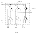
- each inverter section 32, 42 includes multiple switches 31 which selectively connect one phase of each output 14, 18 to either the first rail 28 or the second rail 30.
- Each switch 31 may be a transistor and further include a diode 33 connected in parallel to the transistor.
- Each switch 31 receives a switching signal 35, 45 to enable or disable conduction through the transistor to selectively connect each phase of the output 14, 18 to the first rail 28 or the second rail 30 of the DC bus 24.
- the processor 38 executes a program stored on a memory device 40, where the program includes a series of instructions executable on the processor 38 to control operation of the motor drive 9. Each program receives a reference signal identifying desired operation of the motor 16 connected to the motor drive 9.
- the processor 38 also receives feedback signals from voltage and/or current sensors positioned within the motor drive 9. Sensors 34 may be provided to measure the voltage and/or current on the DC bus 24, and additional sensors 36, 46 may be provided to measure voltage and/or current on one, two, or all three phases of the outputs, 14 or 18.
- the program executes a control routine responsive to the reference signal and to the feedback signals and generates a desired voltage reference signal 102, 112, see also Figs. 7-10 .
- the processor 38 also executes a modulation routine, such as pulse width modulation (PWM), to generate switching signals, 35 or 45, to control the switches 31 of each inverter section 32 or 42 responsive to the desired voltage reference signal 102, 112.
- PWM pulse width modulation
- FIG. 3 another embodiment of the present invention includes a converter 27, connected to the three phase AC input voltage 12.
- a DC bus 24 distributes the DC voltage from the converter 27 to a first remote device 8 and a second remote device 10.
- the first and second remote devices, 8 and 10 may be, for example, distributed motor drives.
- the first remote device 8 generates a first output 14, illustrated as a three phase AC output voltage, to control a first motor 16, and the second remote device 10 generates a second output 18, also illustrated as a three phase AC output voltage, to control a second motor 20.
- Still other embodiments of the invention may include various configurations of converters, inverters, and/or multiple axis motor drives connected to a common DC bus without deviating from the scope of the invention.
- the output voltage, 14 or 18, for the first or second remote device, 8 or 10 respectively could be a single phase AC output voltage, a multi-phase AC output voltage, or a DC voltage, as required by the motor connected to the drive without deviating from the scope of the invention.
- a converter section 22 converts the AC input voltage 12 to a DC voltage potential present on the DC bus 24.
- the converter section 22 may be either passive or active, where a passive converter utilizes electronic devices such as diodes, which require no control signals, to convert the AC voltage to a DC voltage and an active converter utilizes, for example, transistors, which receive switching signals 25 to turn on and off, to convert the AC voltage to a DC voltage.
- the DC voltage potential is present between a first rail 28 and a second rail 30 of the DC bus 24.
- a DC bus capacitor 26 is connected between the first and second rails, 28 and 30, to reduce the magnitude of the reactive voltage resulting from converting the AC voltage to a DC voltage.
- the DC bus capacitor 26 may be a single capacitor or multiple capacitors connected in parallel, in series, or a combination thereof.
- the converter section 22 includes a processor 21 configured to execute a program stored on a memory device 23. If the converter section 22 is active, the processor may be configured to generate the switching signals 25. The processor may also be configured to generate a synchronizing signal to be output to each of the remote devices via, for example, the communication media 17.
- Each of the remote devices 8, 10 includes a DC bus 24 electrically connected to the DC bus 24 of the converter 27.
- each inverter section 32, 42 includes multiple switches 31 which selectively connect one of the output phases 14 to either the first rail 28 or the second rail 30.
- Each switch 31 may be a transistor and further include a diode 33 connected in parallel to the transistor.
- Each switch 31 receives a switching signal 35, 45 to enable or disable conduction through the transistor to selectively connect each phase of the output 14, 18 to the first rail 28 or the second rail 30 of the DC bus 24.
- Each remote device 8, 10 also includes a processor 38, 48 configured to execute a program stored on a memory device 40, 50.
- the program includes a series of instructions executable on the processor 38, 48 to control operation of the remote device 8, 10.
- Each program receives a reference signal identifying desired operation of the motor 16, 20 connected to the remote device 8, 10.
- the reference signal may be, for example, a desired speed or torque and may be transmitted via communication media 17 from the converter 27 or from another controller.
- Each processor 38, 48 also receives feedback signals from voltage and/or current sensors. Sensors 34, 44 may be provided to measure the voltage and/or current on the DC bus 24, and additional sensors 36, 46 may be provided to measure voltage and/or current on one, two, or all three phases of the outputs 14, 18.
- the program executes a control routine responsive to the reference signal and to the feedback signals and generates a desired voltage reference signal 102, 112, see also Figs. 7-10 .
- the processor 38, 48 also executes a modulation routine, such as pulse width modulation (PWM), to generate the switching signals 35, 45 to control the switches of each inverter section 32, 42 responsive to the desired voltage reference
- a controller executes to coordinate the modulation routines of each inverter section 32, 42 to reduce the magnitude of reactive current present on the DC bus 24.
- a single processor 38 may be used.
- the processor 38 may be configured to execute the modulation routines and generate switching signals 35, 45 to each inverter section 32, 42 or optionally, dedicated hardware, such as an FPGA, ASIC, or motor controller may be configured to execute each modulation routine and the processor 38 may be configured to coordinate operation of the modulation routines.
- the converter 27 and each remote device 8, 10 may each include a processor 21, 38, and 48 respectively.
- One of the processors 21, 38, and 48 may be configured to coordinate operation of each of the other processors 21, 38, and 48 or, optionally, still another control device may coordinate operation of each of the processors 21, 38, and 48.
- controllers There are, therefore, various configurations and arrangements of controllers. The present invention will be discussed with respect to Fig. 3 ; however, the illustrated embodiment is not meant to be limiting.
- One of the processors in the system is configured to be a master processor.
- the processor 21 in the converter 27 will be designated as the master processor.
- one of the processors 38, 48 in the remote devices may be designated as the master processor.
- the master processor 21 generates a synchronizing signal, which is transmitted to each of the remote devices 8, 10.
- the synchronizing signal is used by each of the remote devices 8, 10 to coordinate their respective modulation routines.
- the synchronizing signal may be any suitable signal, such as a single pulse or a counter preset value.
- the synchronizing signal may be sent initially upon power up, at the start of operation of a remote device 8, 10, at a periodic interval or any combination thereof.
- modulation routines repeatedly execute at a predefined interval known as a switching period, T, which is the inverse of the switching frequency.
- T a switching period
- Each remote device 8, 10 uses the synchronizing signal to coordinate the start of the switching period T, of its respective modulation routine with the other remote devices 8, 10.
- the start of the switching period, T, for each remote device 8, 10 begins at substantially the same time.
- each processor 38, 48 executes the modulation routine at substantially the same switching frequency such that the duration of the switching period, T, for each remote device 8, 10 is substantially the same.
- the modulation routines for each remote device 8, 10 continue to operation in tandem.
- each processor 38, 48 may be configured to execute the modulation routine at switching frequencies that are multiples of each other, such as 2 kHz and 4 kHz. Because the largest components of the reactive currents typically occur at multiples of the switching frequency, processors 38, 48 having switching frequencies executing at multiples of each other generate at least a portion of their harmonic components of reactive current at like frequencies.
- each processor 38, 48 in each remote device 8, 10 generates a carrier signal 100, 110 for use by a modulation routine.
- the modulation routine of the first inverter section 32 generates a first carrier signal 100
- the modulation routine of the second inverter section 42 generates a second carrier signal 110.
- Each reference signal 100, 110 is repeated within each switching period, T.
- each carrier signal 100, 110 is a triangular waveform, having a maximum value and a minimum value symmetrical about zero.
- the period, T is defined as having three hundred sixty degrees, similar to a sinusoidal waveform with zero degrees defining the start of a period and 360 degrees defining the end of a period.
- each of the carrier signals 100, 110 have a carrier phase angle of zero degrees. Setting the carrier phase angle to a value other zero degrees, shifts the carrier signal 100, 110 within the period, T. For example, in fig. 6 , the carrier phase angle of the first carrier signal 100 remains at zero degrees but the carrier phase angle of the second carrier signal 110 is set to ninety degrees. As a result, the periodic waveform is shifted by one quarter of the period, T.
- the processor 38, 48 in each remote device 8, 10 executes the modulation routine to generate switching signals 35, 45 to control the switches in the respective inverter section 32, 42 as a function of the carrier signals 100, 110.
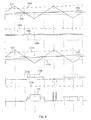
- execution of two periods of a modulation routine is illustrated.
- a control module executing on the first processor 38 generates a first voltage reference signal 102a-c for each phase of the output 14 of the first remote device 8
- a control module executing on the second processor 48 generates a second voltage reference signal 112a-c for each phase of the output 18 of the second remote device 10.
- Each of the voltage reference signals 102a-c, 112a-c is compared against the respective carrier signal 100, 110.
- the modulation routine When the voltage reference signal 102a-c, 112a-c for one of the phases is greater than the respective carrier signal 100, 110, the modulation routine generates switching signals 35, 45 to connect the corresponding phase of the output 14, 18 to the DC bus 24.
- that phase conducts current 104, 114 to the respective motor 16, 20 connected to the remote device 8, 10.
- Exemplary waveforms for the currents 104a-c, 114a-c present on each phase of the output 14, 18 are illustrated below the corresponding waveform illustrating the comparison of the voltage reference signals 102a-c, 112a-c to the carrier signals 100, 110.
- the final waveform illustrates the DC bus current 120, I DC , present on the DC bus 24 as a result of the high frequency switching by each of the inverter sections 32, 42 in the remote devices 8, 10.
- Each of the graphs in Figs. 7-10 illustrates a different set of operating conditions for the two remote devices 8, 10.
- the inverter sections 32, 42 of each remote device 8, 10 use the synchronizing signal to coordinate the start of the switching period, T, of its respective modulation routine, and the switching period, T, for each inverter section 32, 42 is set to the same duration.
- each of the motors 16, 20 controlled by the remote devices 8, 10 are operating in a motoring mode, and the carrier phase angle for the carrier signals 100, 110 generated by each processor 38, 48 is set to zero degrees. As a result, each carrier signal 100, 110 is in phase with the other.
- the voltage references 102a-c, 112a-c for each of the respective inverter sections 32, 42 are substantially the same resulting in output currents 104a-c, 114a-c for each remote device 8, 10 that are substantially the same.
- the reactive current generated by each inverter section 32, 42 is substantially in phase and has similar magnitudes.
- the DC bus current 120 therefore, has an increase in the total reactive current present compared to the reactive current that would be generated by either inverter section 32, 42 operating alone.
- each of the motors 16, 20 controlled by the remote devices 8, 10 are still operating in a motoring mode in Fig. 8 ; however, the carrier phase angle of the first carrier signal 100 is set to zero degrees and the carrier phase angle of the second carrier signal 110 is set to ninety degrees.
- the currents 104a-c generated by the first inverter section 32 are the same as illustrated in Fig. 7 . However, the output currents 114a-c generated by the second inverter section 42 are shifted in phase as a result of the carrier phase angle offset. As a result, the reactive currents generated by each inverter section 32, 42 are out of phase with each other, and the reactive current generated by the second inverter section 42 at least partially cancels the reactive current generated by the first inverter section 32.
- the DC bus current 120 therefore, has a lower total reactive current present compared to the reactive current that would be generated by either inverter section 32, 42 operating alone.
- the motor 16 controlled by the first remote device 8 is operating in a motoring mode; however, the motor 20 controlled by the second remote device 10 is operating in a regenerative mode.
- the carrier phase angle for the carrier signals 100, 110 generated by each processor 38, 48 is set to zero degrees.
- the reactive current generated by the second inverter section 42 is out of phase with the reactive current generated by the first inverter section 32 and, therefore, the reactive current generated by the second inverter section 42 at least partially cancels the reactive current generated by the first inverter section 32.
- the DC bus current 120 therefore, has a lower total reactive current present compared to the reactive current that would be generated by either inverter section 32, 42 operating alone.
- the carrier phase angle of the first carrier signal 100 is set to zero degrees and the carrier phase angle of the second carrier signal 110 is set to ninety degrees.
- the output currents 114a-c generated by the second inverter section 42 are still shifted as a result of the carrier phase angle offset, the reactive current generated by each inverter section 32, 42 is substantially in phase.
- the DC bus current 120 therefore, has an increase in the total reactive current present compared to the reactive current that would be generated by either inverter section 32, 42 operating alone.
- selection of a carrier phase angle for each of the carrier signals 100, 110 in a remote device 8, 10 is a function of whether the corresponding motor 16, 20 controlled by the remote device 8, 10 is operating in a motoring mode or in a regenerating mode.
- each motor 16, 20 may transition between the motoring mode and the regenerating mode while continuing to rotate due, for example, to a change in the load on the motor 16, 20 or to a change in the commanded speed of the motor 16, 20.
- the carrier phase angle for the carrier signals 100, 110 generated by each processor 38, 48 therefore, may also be modified during operation such that the reactive currents generated by each remote device 8, 10 continue to cancel each other regardless of the operating mode of the motors 16, 20.
- the carrier phase angle selected for each of the carrier signals 100, 110 is also a function of the number of inverter sections connected to the common DC bus.
- any number of inverters 15 may be connected to the DC bus 13.
- the total current, I DC present on the shared DC bus 13 is equal to the sum of the currents (e.g., 1 1 + I 2 + ⁇ + I n ) required by each of the inverters 15.
- the reactive current generated by each of the inverters 15 is also present on the DC bus 13 and the total reactive current present on the shared DC bus 13 is the sum of the reactive currents generated by each of the inverters 15.
- the effect of the reactive current from varying numbers of inverters 15 is illustrated, for example in Figs.
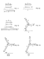
- an alternating current may be represented as a phasor quantity having an amplitude and an angle.
- Fig. 11 two inverters 15 are connected to the DC bus and the reactive current generated by each of the inverters 15 is represented as a current having a magnitude equal to "A" and an angle of zero degrees.
- the resulting reactive current at the output of the converter 11 has a magnitude equal to "2A” or twice the magnitude of each of the inverters 15 at an angle of zero degrees.
- Fig. 13 three inverters 15 are connected to the DC bus and the reactive current generated by each of the inverters 15 is represented as a current having a magnitude equal to "A” and an angle of zero degrees.
- the resulting reactive current at the output of the converter 11 has a magnitude equal to "3A" or three times the magnitude of each of the inverters 15 at an angle of zero degrees.
- the phase angle of the reactive current generated from each of the inverters 15 is controlled such that the total reactive current on the shared DC bus 13 is reduced.
- Figs. 12 and 14 the effect of controlling the phase angle of the reactive current on the total reactive current is illustrated.
- Fig. 12 two inverters 15 are connected to the DC bus.
- the carrier phase angle of the first inverter 15 is set to zero degrees, and the reactive current generated by a first inverter 15 has a magnitude equal to "A" and an angle of zero degrees.
- the carrier phase angle of the second inverter 15 is set to ninety degrees, and the reactive current generated by the second inverter 15 has a magnitude equal to "A" and an angle of one hundred eighty degrees. Consequently, the reactive current generated by the second inverter cancels the reactive current generated by the first inverter and the resulting reactive current on the shared DC bus 13 is zero.
- three inverters 15 are connected to the DC bus.
- the carrier phase angle of the first inverter is set to zero degrees, and the reactive current generated by the first inverter 15 has a magnitude equal to "A" and an angle of zero degrees.
- the carrier phase angle of the second inverter is set to sixty degrees, and the reactive current generated by the first inverter 15 has a magnitude equal to "A" and an angle of one hundred twenty degrees.
- the carrier phase angle of the third inverter is set to one hundred twenty degrees, and the reactive current generated by the third inverter 15 has a magnitude equal to "A" and an angle of two hundred forty degrees. Consequently, the reactive currents generated by the three inverters cancel each other and the resulting reactive current on the shared DC bus 13 is zero.
- Figs. 12 and 14 represent idealized cancellation of reactive current and actual magnitudes and phases of the reactive currents generated by the inverters may vary.
- the magnitude of the resulting reactive current on the shared DC bus I is less than magnitude of the reactive current that would be present if any one of the inverters 15 is operating by itself.
- a preset value of the carrier phase angle may be assigned to each inverter 15 connected to the DC bus 13.
- the memory device 40, 50 in each of the remote devices 8, 10 may store the assigned carrier phase angle and the respective processor 38, 48 may retrieve the stored value for generation of the carrier signal.
- the value of the carrier phase angle may be selected as a function of the switching frequency or multiples thereof, the output frequency or multiples thereof, the number of remote devices 8, 10 connected to the common DC bus 24, the operating mode of a motor 16, 20 controlled by one of the remote devices 8, 10, or a combination thereof.
- the value of the carrier phase angle may be dynamically determined for each of the remote devices 8, 10.
- the memory device 40, 50 in each of the remote devices 8, 10 may have, for example, a look-up table in which multiple carrier phase angle values are stored.
- the carrier phase angle for each of the remote devices 8, 10 may be a first value if two inverter sections 32, 42 are connected to the DC bus 24 and a different value for each additional inverter section that is connected to the DC bus 24.
- three or more inverter sections may be connected but not all enabled at the same time to control their respective AC motor.
- the communication media 17 between processors may transmit data indicating the number of inverter sections that are currently enabled.
- the carrier phase angle for each device may be dynamically updated as different inverter sections are enabled and disabled. Further, the switching frequency of different inverter sections 32, 42 may be set to different values.
- the communication media 17 may also transmit data indicating the switching frequency of each inverter section.
- the inverter sections 32, 42 may then determine a carrier phase angle for each inverter section as a function of the number of inverter sections 32, 42 having either the same switching frequency or switching frequencies at multiples of each other.
- the processor 38, 48 in each remote device 8, 10 determines the carrier phase angle for the respective device.
- each of the processors 38, 48 transmit the operating status of the device to a master processor, which may be, for example, the processor 21 in the converter 27, and the master processor determines the carrier phase angle for each device and transmits the carrier phase angle to the respective devices.
- a master processor which may be, for example, the processor 21 in the converter 27, and the master processor determines the carrier phase angle for each device and transmits the carrier phase angle to the respective devices.
- the processor 38, 48 may measure the current present on the DC bus 24 and determine the carrier phase angle of each of the devices.
- the processor 38, 48 receives a feedback signal corresponding to the current present on the DC bus 24.
- the processor 38, 48 determines the spectral content of the feedback signal which contains amplitude information for varying frequencies present on the DC bus 24.
- the spectral content may be determined, for example, using a fourier transform, which may be a function of the output frequency and/or the switching frequency.
- a high frequency component of the current may be identified from the spectral content, for example, according to the component having the greatest amplitude.
- the phase of the identified frequency component may then be determined.
- Multiple processors 38, 48 communicate between each other the respective amplitude and/or phase of the identified frequency component to be compensated.
- the magnitude of the reactive current may be estimated as a function of the operating parameters conditions of each inverter section 32, 42.
- the processor 38, 42 receives a reference signal identifying desired operation of the motor 16 which is used to control operation of the motor drive 9.
- the reference signal may be, for example, a desired torque, speed, or angular position of the motor.
- the program generates, for example, an internal torque or current reference which is provided to a current regulator.
- the current regulator generates the desired voltage reference signal 102, 112 provided to the PWM module.
- each processor 38, 42 may be configured to determine an expected magnitude of reactive current.
- the carrier phase angle for each inverter section 32, 42 may then be determined to provide the best reduction of total reactive current on the DC bus 24 as a function of the measured current, estimated current, or a combination thereof.
- three inverters 15 are connected to the DC bus 13. Each of the inverters 15 determine that they are generating a reactive current at substantially the same frequency with magnitudes of "A", "B", and "C".
- the carrier phase angles of the inverters are set such that the phase angle of the respective reactive currents are zero degrees, one hundred twenty degrees, or two hundred forty degrees, as discussed above with respect to Fig. 14
- the resulting reactive current may have, for example, a magnitude equal to "D" at zero degrees as shown in Fig. 15 .
- the magnitude of"D" is less than the largest magnitude of the reactive current generated by any one of the inverters 15, it may not be the best obtainable reduction in reactive current.
- the carrier phase angle of the inverters 15 may be set such that the phase angle of each reactive current is zero degrees, ninety degrees, and two hundred thirty degrees.
- the resulting reactive current on the DC bus has a magnitude of "E” at zero degrees, where the magnitude of "E” is less than the magnitude of "D".
- the carrier phase angle may also be determined as a function of the magnitude of the reactive current generated by the inverters 15.
- one of the processors may be configured to generate carrier phase angles for each inverter 15.
- a control routine receives a reference corresponding, for example, to a desired magnitude of reactive current or a desired percentage reduction in the reactive current.
- the reactive current either measured or estimated at each inverter 15 is transmitted to the processor generating carrier phase angles.
- the control routine then generates carrier phase angles at which each inverter is to operate as a function or the reactive current and the reference signal.
- the carrier phase angle may be utilized to reduce conducted emissions generated by the inverters 15.
- the high frequency content of the reactive current may result in radiated and/or conducted emissions that are coupled back to the AC input voltage.
- leakage currents may be established through capacitive coupling between leads and the ground connections. If left unmitigated, these conducted emissions could interfere with other electrical devices receiving the same input voltage or connected elsewhere within the facility.
- the carrier phase angles of two inverters 15 operating under substantially identical operating conditions are set one hundred eighty degrees apart from each other, the emissions generated by the first inverter will offset the emissions generated by the second inverter. If more than two inverters 15 exist in the system, the carrier phase angle of a portion of the inverters 15 may be set to zero degrees and the carrier phase angle of the remaining inverters 15 may be set to one hundred eighty degrees.
- the reactive current may be amplified by setting the carrier phase angle of a first inverter 15 to zero degrees and a second inverter 15 to one hundred eighty degrees.
- the processor configured to generate carrier phase angles for each inverter 15 may further monitor the magnitude of current supplied by each inverter 15 to its corresponding motor to determine a desired operating mode. If for example, the current output to the motor is below a threshold, such as fifty percent of rated current for the inverter 15, the carrier phase angle may be controlled to minimize the conducted emissions generated by the inverter 15. If, however, the current output to the motor is above the threshold, the carrier phase angle may be controlled to minimize the reactive current on the DC bus 13.
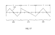
- the processor may generate a transitional carrier signal during a transition between carrier phase angles.
- the inverter 15 is in a first operating mode and has determined a first carrier phase angle at which the carrier signal is to be generated.
- the operating conditions of the system change, for example, due to the motor controlled by an inverter 15 switching between motoring and regenerative operation or by the addition or subtraction of an enabled inverter 15 connected to the DC bus 13.
- a new carrier phase angle is determined for operation in a second operating mode.
- the carrier signal is changed from a triangle waveform to a ramp waveform.
- the carrier signal preferably remains a ramp waveform for one period 210 and then reverts to a triangle waveform having the new carrier phase angle during the third period 220. This transition between operating modes reduces undesirable step changes in the output of the inverter 15.
Landscapes
- Engineering & Computer Science (AREA)
- Power Engineering (AREA)
- Inverter Devices (AREA)
Applications Claiming Priority (1)
| Application Number | Priority Date | Filing Date | Title |
|---|---|---|---|
| US13/910,656 US9515484B2 (en) | 2013-06-05 | 2013-06-05 | System and method for reducing reactive current on a common DC bus with multiple inverters |
Publications (3)
| Publication Number | Publication Date |
|---|---|
| EP2811633A2 true EP2811633A2 (fr) | 2014-12-10 |
| EP2811633A3 EP2811633A3 (fr) | 2015-07-15 |
| EP2811633B1 EP2811633B1 (fr) | 2021-04-14 |
Family
ID=50842188
Family Applications (1)
| Application Number | Title | Priority Date | Filing Date |
|---|---|---|---|
| EP14171100.2A Active EP2811633B1 (fr) | 2013-06-05 | 2014-06-04 | Système et procédé de réduction de courant réactif sur un bus CC commun à plusieurs onduleurs |
Country Status (3)
| Country | Link |
|---|---|
| US (1) | US9515484B2 (fr) |
| EP (1) | EP2811633B1 (fr) |
| CN (1) | CN104242739A (fr) |
Cited By (6)
| Publication number | Priority date | Publication date | Assignee | Title |
|---|---|---|---|---|
| WO2018054544A1 (fr) * | 2016-09-22 | 2018-03-29 | Sew-Eurodrive Gmbh & Co. Kg | Système comprenant un premier onduleur et un second onduleur, et procédé de fonctionnement du système |
| DE102016124099A1 (de) * | 2016-12-12 | 2018-06-14 | Ebm-Papst Mulfingen Gmbh & Co. Kg | EMV-Kühlgerät |
| WO2018166650A1 (fr) * | 2017-03-14 | 2018-09-20 | Diehl Ako Stiftung & Co. Kg | Procédé pour faire fonctionner un premier convertisseur et un deuxième convertisseur |
| EP3425786A1 (fr) * | 2017-07-03 | 2019-01-09 | Hamilton Sundstrand Corporation | Système d'entraînement de moteur |
| DE102020124496A1 (de) | 2020-09-21 | 2022-03-24 | Audi Aktiengesellschaft | Verfahren zum Betreiben von wenigstens zwei mit einem Gleichstromnetzwerk verbundenen Wechselrichtern und Kraftfahrzeug |
| DE102022206581A1 (de) * | 2022-06-29 | 2024-01-04 | Zf Friedrichshafen Ag | Verfahren zur Steuerung des Betriebs einer elektrischen Anordnung |
Families Citing this family (21)
| Publication number | Priority date | Publication date | Assignee | Title |
|---|---|---|---|---|
| DE102013225603B4 (de) * | 2013-12-11 | 2015-07-16 | Siemens Aktiengesellschaft | Stromrichtervorrichtung für eine Ein- oder Mehrachsanordnung und Betriebsverfahren |
| JP6424486B2 (ja) * | 2014-06-18 | 2018-11-21 | 富士電機株式会社 | 電力変換装置の多重化システム |
| US9882421B2 (en) * | 2015-05-14 | 2018-01-30 | Rockwell Automation Technologies, Inc. | Method and apparatus for increasing current capacity of a distributed drive system |
| EP3213952B1 (fr) * | 2016-03-02 | 2020-08-26 | Airbus Defence and Space GmbH | Systeme d'entrainement electrique pour un aeronef et procede de fonctionnement |
| US10291147B2 (en) * | 2016-09-29 | 2019-05-14 | Ge Global Sourcing Llc | Current reduction system for inverters connected to a common bus |
| US12573965B2 (en) | 2016-09-29 | 2026-03-10 | Transportation Ip Holdings, Llc | Harmonic distortion reduction system for converters connected to a common bus |
| EP3324527B1 (fr) | 2016-11-18 | 2021-06-30 | Aros Electronics AB | Élimination d'ondulation de bus cc pour machines électriques polyphasées |
| DE102016223349A1 (de) * | 2016-11-24 | 2018-05-24 | Brose Fahrzeugteile GmbH & Co. Kommanditgesellschaft, Würzburg | Verfahren zum Betrieb eines bürstenlosen Elektromotors eines Kraftfahrzeugs |
| US10291145B2 (en) | 2016-12-14 | 2019-05-14 | Caterpillar Inc. | Inverter assembly for electric power system |
| US10581361B2 (en) * | 2017-01-17 | 2020-03-03 | Ford Global Technologies, Llc | Multiple inverter system for an electric machine |
| JP6383028B2 (ja) * | 2017-02-10 | 2018-08-29 | ファナック株式会社 | モータ駆動装置 |
| WO2018191108A1 (fr) * | 2017-04-12 | 2018-10-18 | General Electric Company | Système de réduction de courant pour onduleurs connectés à un bus commun |
| JP7007577B2 (ja) * | 2018-02-26 | 2022-01-24 | ダイキン工業株式会社 | Ac-ac変換装置、電力変換装置 |
| CN111082710A (zh) * | 2019-12-25 | 2020-04-28 | 深圳万讯自控股份有限公司 | 一种伺服电机直流母线载波控制拓扑结构及方法 |
| CN115835975A (zh) * | 2020-07-17 | 2023-03-21 | 康明斯公司 | 减少dc链路中的纹波电流的同步多逆变器系统 |
| US11664743B2 (en) | 2020-08-14 | 2023-05-30 | Ut-Battelle, Llc | System and method of inverter control |
| US12438435B2 (en) | 2020-10-01 | 2025-10-07 | Vestas Wind Systems A/S | Method for reduction of DC link busbar and capacitor current, by adjustment of a PWM carrier delay |
| EP4047809B1 (fr) | 2021-02-22 | 2025-07-23 | Hamilton Sundstrand Corporation | Architecture de distribution de commande |
| US11539283B1 (en) * | 2021-06-04 | 2022-12-27 | Rockwell Automation Technologies, Inc. | System and method for reducing delay in the modulation of a multi-phase output voltage from an inverter |
| CN113595054A (zh) * | 2021-08-24 | 2021-11-02 | 深圳市宝来威智能科技有限公司 | 一种新型低压直流大功率两线制控制系统 |
| US12531496B2 (en) * | 2023-09-08 | 2026-01-20 | Rockwell Automation Technologies, Inc. | System and method for reducing energy loss from multiple inverters utilizing a shared DC bus |
Family Cites Families (15)
| Publication number | Priority date | Publication date | Assignee | Title |
|---|---|---|---|---|
| US4628460A (en) * | 1982-09-17 | 1986-12-09 | Eaton Corporation | Microprocessor controlled phase shifter |
| US5408404A (en) | 1993-03-25 | 1995-04-18 | Rockwell International Corp. | High frequency interleaved DC-to-AC power converter apparatus |
| JP3555567B2 (ja) | 2000-09-04 | 2004-08-18 | 日産自動車株式会社 | 回転電機の制御装置 |
| US6864646B2 (en) | 2003-02-14 | 2005-03-08 | General Motors Corporation | Multiple inverter system with low power bus ripples and method therefor |
| JP2004274842A (ja) * | 2003-03-06 | 2004-09-30 | Suzuki Motor Corp | 交流発電機の発電制御装置 |
| US6897698B1 (en) | 2003-05-30 | 2005-05-24 | O2Micro International Limited | Phase shifting and PWM driving circuits and methods |
| US7425806B2 (en) | 2004-04-12 | 2008-09-16 | York International Corporation | System and method for controlling a variable speed drive |
| US7295448B2 (en) | 2004-06-04 | 2007-11-13 | Siemens Vdo Automotive Corporation | Interleaved power converter |
| TWI265675B (en) | 2004-10-22 | 2006-11-01 | Chung Shan Inst Of Science | Interleaving control type inverter |
| JP2006149141A (ja) * | 2004-11-24 | 2006-06-08 | Nippon Densan Corp | モータ駆動制御方法及びモータ駆動制御装置 |
| US8421393B2 (en) * | 2007-10-19 | 2013-04-16 | Lockheed Martin Corporation | System and method for pulse edge synchronization |
| DE102008037543A1 (de) * | 2007-12-28 | 2009-07-02 | DENSO CORPORARTION, Kariya-shi | Motorsteuervorrichtung, Fahrzeuglüfter-Ansteuervorrichtung und Motorsteuerverfahren |
| CN101860319B (zh) * | 2010-06-01 | 2012-05-23 | 华东交通大学 | 一种多目标的大功率逆变器共模电压抑制方法 |
| US8963453B2 (en) * | 2010-12-16 | 2015-02-24 | Rockwell Automation Technologies, Inc. | Method and apparatus for synchronization of pulse width modulation |
| FR2979493B1 (fr) | 2011-08-25 | 2013-09-13 | Converteam Technology Ltd | Compensateur d'energie reactive comprenant n onduleurs en parallele, n bancs de condensateur(s) et des moyens de connexion des bancs au travers de composants electriques passifs |
-
2013
- 2013-06-05 US US13/910,656 patent/US9515484B2/en active Active
-
2014
- 2014-06-04 EP EP14171100.2A patent/EP2811633B1/fr active Active
- 2014-06-05 CN CN201410246629.4A patent/CN104242739A/zh active Pending
Non-Patent Citations (1)
| Title |
|---|
| None |
Cited By (10)
| Publication number | Priority date | Publication date | Assignee | Title |
|---|---|---|---|---|
| WO2018054544A1 (fr) * | 2016-09-22 | 2018-03-29 | Sew-Eurodrive Gmbh & Co. Kg | Système comprenant un premier onduleur et un second onduleur, et procédé de fonctionnement du système |
| US11121636B2 (en) | 2016-09-22 | 2021-09-14 | Sew-Eurodrive Gmbh & Co. Kg | System including a first inverter and a second inverter, and method for operating the system |
| US12308756B2 (en) | 2016-09-22 | 2025-05-20 | Sew-Eurodrive Gmbh & Co. Kg | System including a first inverter and a second inverter, and method for operating the system |
| DE102016124099A1 (de) * | 2016-12-12 | 2018-06-14 | Ebm-Papst Mulfingen Gmbh & Co. Kg | EMV-Kühlgerät |
| WO2018166650A1 (fr) * | 2017-03-14 | 2018-09-20 | Diehl Ako Stiftung & Co. Kg | Procédé pour faire fonctionner un premier convertisseur et un deuxième convertisseur |
| EP3425786A1 (fr) * | 2017-07-03 | 2019-01-09 | Hamilton Sundstrand Corporation | Système d'entraînement de moteur |
| US10536099B2 (en) | 2017-07-03 | 2020-01-14 | Hamilton Sundstrand Corporation | Motor drive system |
| DE102020124496A1 (de) | 2020-09-21 | 2022-03-24 | Audi Aktiengesellschaft | Verfahren zum Betreiben von wenigstens zwei mit einem Gleichstromnetzwerk verbundenen Wechselrichtern und Kraftfahrzeug |
| US11921538B2 (en) | 2020-09-21 | 2024-03-05 | Audi Ag | Method for operating at least two inverters connected to a direct current network and motor vehicle |
| DE102022206581A1 (de) * | 2022-06-29 | 2024-01-04 | Zf Friedrichshafen Ag | Verfahren zur Steuerung des Betriebs einer elektrischen Anordnung |
Also Published As
| Publication number | Publication date |
|---|---|
| US20140361613A1 (en) | 2014-12-11 |
| CN104242739A (zh) | 2014-12-24 |
| EP2811633A3 (fr) | 2015-07-15 |
| EP2811633B1 (fr) | 2021-04-14 |
| US9515484B2 (en) | 2016-12-06 |
Similar Documents
| Publication | Publication Date | Title |
|---|---|---|
| US9515484B2 (en) | System and method for reducing reactive current on a common DC bus with multiple inverters | |
| JP4433099B1 (ja) | 電力変換装置 | |
| US8963453B2 (en) | Method and apparatus for synchronization of pulse width modulation | |
| JP5377604B2 (ja) | 電力変換装置 | |
| JP5377603B2 (ja) | 電力変換装置 | |
| EP0555557A1 (fr) | Dispositif de réglage d'un convertisseur | |
| JP2017192196A (ja) | 交流電動機の制御装置 | |
| EP3404820B1 (fr) | Système de conversion de puissance et dispositif de conversion de puissance | |
| JPS63287397A (ja) | 誘導電動機の制御装置 | |
| WO2014136142A1 (fr) | Système pour commander un moteur à courant alternatif | |
| KR101579390B1 (ko) | 전력 변환 장치 | |
| JP2013055868A5 (fr) | ||
| JP2013055866A5 (fr) | ||
| AU2017336112A1 (en) | Control device for power converter | |
| US20130307463A1 (en) | Power conversion apparatus, power conversion method, motor system, and two-phase induction motor | |
| JP7078869B2 (ja) | 電力変換システム | |
| JP2013055864A5 (fr) | ||
| CN116613972A (zh) | 电源转换器中的谐波干扰的减轻 | |
| US9543849B2 (en) | Power conversion apparatus, power conversion method, motor system, and three-phase motor | |
| CN118399728A (zh) | 延长功率转换器中的电容器寿命 | |
| US10122253B2 (en) | Power conversion apparatus and initial charging method of the same | |
| JP6150946B2 (ja) | 電気車の制御装置 | |
| Kumar et al. | A Zig-Zag Transformer and Three-leg VSC Based DSTATCOM for a Diesel Generator Based Microgrid | |
| KR101427629B1 (ko) | 다상발전기 동체 및 커패시터리스 제어기를 적용한 발전기 시스템 | |
| JP2020108273A (ja) | 電力分配システム |
Legal Events
| Date | Code | Title | Description |
|---|---|---|---|
| PUAI | Public reference made under article 153(3) epc to a published international application that has entered the european phase |
Free format text: ORIGINAL CODE: 0009012 |
|
| 17P | Request for examination filed |
Effective date: 20140604 |
|
| AK | Designated contracting states |
Kind code of ref document: A2 Designated state(s): AL AT BE BG CH CY CZ DE DK EE ES FI FR GB GR HR HU IE IS IT LI LT LU LV MC MK MT NL NO PL PT RO RS SE SI SK SM TR |
|
| AX | Request for extension of the european patent |
Extension state: BA ME |
|
| RIN1 | Information on inventor provided before grant (corrected) |
Inventor name: HUANG, RONGJUN Inventor name: WINTERHALTER, CRAIG Inventor name: GRIES, MARK Inventor name: LI, YE |
|
| PUAL | Search report despatched |
Free format text: ORIGINAL CODE: 0009013 |
|
| AK | Designated contracting states |
Kind code of ref document: A3 Designated state(s): AL AT BE BG CH CY CZ DE DK EE ES FI FR GB GR HR HU IE IS IT LI LT LU LV MC MK MT NL NO PL PT RO RS SE SI SK SM TR |
|
| AX | Request for extension of the european patent |
Extension state: BA ME |
|
| RIC1 | Information provided on ipc code assigned before grant |
Ipc: H02M 1/00 20070101ALI20150610BHEP Ipc: H02M 7/493 20070101ALI20150610BHEP Ipc: H02M 1/14 20060101AFI20150610BHEP |
|
| R17P | Request for examination filed (corrected) |
Effective date: 20160115 |
|
| RBV | Designated contracting states (corrected) |
Designated state(s): AL AT BE BG CH CY CZ DE DK EE ES FI FR GB GR HR HU IE IS IT LI LT LU LV MC MK MT NL NO PL PT RO RS SE SI SK SM TR |
|
| STAA | Information on the status of an ep patent application or granted ep patent |
Free format text: STATUS: EXAMINATION IS IN PROGRESS |
|
| 17Q | First examination report despatched |
Effective date: 20170215 |
|
| GRAP | Despatch of communication of intention to grant a patent |
Free format text: ORIGINAL CODE: EPIDOSNIGR1 |
|
| STAA | Information on the status of an ep patent application or granted ep patent |
Free format text: STATUS: GRANT OF PATENT IS INTENDED |
|
| INTG | Intention to grant announced |
Effective date: 20200806 |
|
| GRAJ | Information related to disapproval of communication of intention to grant by the applicant or resumption of examination proceedings by the epo deleted |
Free format text: ORIGINAL CODE: EPIDOSDIGR1 |
|
| STAA | Information on the status of an ep patent application or granted ep patent |
Free format text: STATUS: EXAMINATION IS IN PROGRESS |
|
| GRAP | Despatch of communication of intention to grant a patent |
Free format text: ORIGINAL CODE: EPIDOSNIGR1 |
|
| STAA | Information on the status of an ep patent application or granted ep patent |
Free format text: STATUS: GRANT OF PATENT IS INTENDED |
|
| INTC | Intention to grant announced (deleted) | ||
| INTG | Intention to grant announced |
Effective date: 20201125 |
|
| GRAS | Grant fee paid |
Free format text: ORIGINAL CODE: EPIDOSNIGR3 |
|
| GRAA | (expected) grant |
Free format text: ORIGINAL CODE: 0009210 |
|
| STAA | Information on the status of an ep patent application or granted ep patent |
Free format text: STATUS: THE PATENT HAS BEEN GRANTED |
|
| AK | Designated contracting states |
Kind code of ref document: B1 Designated state(s): AL AT BE BG CH CY CZ DE DK EE ES FI FR GB GR HR HU IE IS IT LI LT LU LV MC MK MT NL NO PL PT RO RS SE SI SK SM TR |
|
| REG | Reference to a national code |
Ref country code: GB Ref legal event code: FG4D |
|
| REG | Reference to a national code |
Ref country code: CH Ref legal event code: EP |
|
| REG | Reference to a national code |
Ref country code: DE Ref legal event code: R096 Ref document number: 602014076529 Country of ref document: DE |
|
| REG | Reference to a national code |
Ref country code: IE Ref legal event code: FG4D |
|
| REG | Reference to a national code |
Ref country code: AT Ref legal event code: REF Ref document number: 1383354 Country of ref document: AT Kind code of ref document: T Effective date: 20210515 |
|
| REG | Reference to a national code |
Ref country code: LT Ref legal event code: MG9D |
|
| REG | Reference to a national code |
Ref country code: AT Ref legal event code: MK05 Ref document number: 1383354 Country of ref document: AT Kind code of ref document: T Effective date: 20210414 |
|
| REG | Reference to a national code |
Ref country code: NL Ref legal event code: MP Effective date: 20210414 |
|
| PG25 | Lapsed in a contracting state [announced via postgrant information from national office to epo] |
Ref country code: NL Free format text: LAPSE BECAUSE OF FAILURE TO SUBMIT A TRANSLATION OF THE DESCRIPTION OR TO PAY THE FEE WITHIN THE PRESCRIBED TIME-LIMIT Effective date: 20210414 Ref country code: LT Free format text: LAPSE BECAUSE OF FAILURE TO SUBMIT A TRANSLATION OF THE DESCRIPTION OR TO PAY THE FEE WITHIN THE PRESCRIBED TIME-LIMIT Effective date: 20210414 Ref country code: FI Free format text: LAPSE BECAUSE OF FAILURE TO SUBMIT A TRANSLATION OF THE DESCRIPTION OR TO PAY THE FEE WITHIN THE PRESCRIBED TIME-LIMIT Effective date: 20210414 Ref country code: AT Free format text: LAPSE BECAUSE OF FAILURE TO SUBMIT A TRANSLATION OF THE DESCRIPTION OR TO PAY THE FEE WITHIN THE PRESCRIBED TIME-LIMIT Effective date: 20210414 Ref country code: BG Free format text: LAPSE BECAUSE OF FAILURE TO SUBMIT A TRANSLATION OF THE DESCRIPTION OR TO PAY THE FEE WITHIN THE PRESCRIBED TIME-LIMIT Effective date: 20210714 Ref country code: HR Free format text: LAPSE BECAUSE OF FAILURE TO SUBMIT A TRANSLATION OF THE DESCRIPTION OR TO PAY THE FEE WITHIN THE PRESCRIBED TIME-LIMIT Effective date: 20210414 |
|
| PG25 | Lapsed in a contracting state [announced via postgrant information from national office to epo] |
Ref country code: GR Free format text: LAPSE BECAUSE OF FAILURE TO SUBMIT A TRANSLATION OF THE DESCRIPTION OR TO PAY THE FEE WITHIN THE PRESCRIBED TIME-LIMIT Effective date: 20210715 Ref country code: LV Free format text: LAPSE BECAUSE OF FAILURE TO SUBMIT A TRANSLATION OF THE DESCRIPTION OR TO PAY THE FEE WITHIN THE PRESCRIBED TIME-LIMIT Effective date: 20210414 Ref country code: IS Free format text: LAPSE BECAUSE OF FAILURE TO SUBMIT A TRANSLATION OF THE DESCRIPTION OR TO PAY THE FEE WITHIN THE PRESCRIBED TIME-LIMIT Effective date: 20210814 Ref country code: PT Free format text: LAPSE BECAUSE OF FAILURE TO SUBMIT A TRANSLATION OF THE DESCRIPTION OR TO PAY THE FEE WITHIN THE PRESCRIBED TIME-LIMIT Effective date: 20210816 Ref country code: NO Free format text: LAPSE BECAUSE OF FAILURE TO SUBMIT A TRANSLATION OF THE DESCRIPTION OR TO PAY THE FEE WITHIN THE PRESCRIBED TIME-LIMIT Effective date: 20210714 Ref country code: PL Free format text: LAPSE BECAUSE OF FAILURE TO SUBMIT A TRANSLATION OF THE DESCRIPTION OR TO PAY THE FEE WITHIN THE PRESCRIBED TIME-LIMIT Effective date: 20210414 Ref country code: ES Free format text: LAPSE BECAUSE OF FAILURE TO SUBMIT A TRANSLATION OF THE DESCRIPTION OR TO PAY THE FEE WITHIN THE PRESCRIBED TIME-LIMIT Effective date: 20210414 Ref country code: SE Free format text: LAPSE BECAUSE OF FAILURE TO SUBMIT A TRANSLATION OF THE DESCRIPTION OR TO PAY THE FEE WITHIN THE PRESCRIBED TIME-LIMIT Effective date: 20210414 Ref country code: RS Free format text: LAPSE BECAUSE OF FAILURE TO SUBMIT A TRANSLATION OF THE DESCRIPTION OR TO PAY THE FEE WITHIN THE PRESCRIBED TIME-LIMIT Effective date: 20210414 |
|
| REG | Reference to a national code |
Ref country code: DE Ref legal event code: R097 Ref document number: 602014076529 Country of ref document: DE |
|
| PG25 | Lapsed in a contracting state [announced via postgrant information from national office to epo] |
Ref country code: SM Free format text: LAPSE BECAUSE OF FAILURE TO SUBMIT A TRANSLATION OF THE DESCRIPTION OR TO PAY THE FEE WITHIN THE PRESCRIBED TIME-LIMIT Effective date: 20210414 Ref country code: SK Free format text: LAPSE BECAUSE OF FAILURE TO SUBMIT A TRANSLATION OF THE DESCRIPTION OR TO PAY THE FEE WITHIN THE PRESCRIBED TIME-LIMIT Effective date: 20210414 Ref country code: EE Free format text: LAPSE BECAUSE OF FAILURE TO SUBMIT A TRANSLATION OF THE DESCRIPTION OR TO PAY THE FEE WITHIN THE PRESCRIBED TIME-LIMIT Effective date: 20210414 Ref country code: CZ Free format text: LAPSE BECAUSE OF FAILURE TO SUBMIT A TRANSLATION OF THE DESCRIPTION OR TO PAY THE FEE WITHIN THE PRESCRIBED TIME-LIMIT Effective date: 20210414 Ref country code: DK Free format text: LAPSE BECAUSE OF FAILURE TO SUBMIT A TRANSLATION OF THE DESCRIPTION OR TO PAY THE FEE WITHIN THE PRESCRIBED TIME-LIMIT Effective date: 20210414 Ref country code: RO Free format text: LAPSE BECAUSE OF FAILURE TO SUBMIT A TRANSLATION OF THE DESCRIPTION OR TO PAY THE FEE WITHIN THE PRESCRIBED TIME-LIMIT Effective date: 20210414 Ref country code: MC Free format text: LAPSE BECAUSE OF FAILURE TO SUBMIT A TRANSLATION OF THE DESCRIPTION OR TO PAY THE FEE WITHIN THE PRESCRIBED TIME-LIMIT Effective date: 20210414 |
|
| REG | Reference to a national code |
Ref country code: CH Ref legal event code: PL |
|
| PLBE | No opposition filed within time limit |
Free format text: ORIGINAL CODE: 0009261 |
|
| STAA | Information on the status of an ep patent application or granted ep patent |
Free format text: STATUS: NO OPPOSITION FILED WITHIN TIME LIMIT |
|
| REG | Reference to a national code |
Ref country code: BE Ref legal event code: MM Effective date: 20210630 |
|
| 26N | No opposition filed |
Effective date: 20220117 |
|
| PG25 | Lapsed in a contracting state [announced via postgrant information from national office to epo] |
Ref country code: LU Free format text: LAPSE BECAUSE OF NON-PAYMENT OF DUE FEES Effective date: 20210604 |
|
| PG25 | Lapsed in a contracting state [announced via postgrant information from national office to epo] |
Ref country code: LI Free format text: LAPSE BECAUSE OF NON-PAYMENT OF DUE FEES Effective date: 20210630 Ref country code: IE Free format text: LAPSE BECAUSE OF NON-PAYMENT OF DUE FEES Effective date: 20210604 Ref country code: CH Free format text: LAPSE BECAUSE OF NON-PAYMENT OF DUE FEES Effective date: 20210630 |
|
| PG25 | Lapsed in a contracting state [announced via postgrant information from national office to epo] |
Ref country code: IS Free format text: LAPSE BECAUSE OF FAILURE TO SUBMIT A TRANSLATION OF THE DESCRIPTION OR TO PAY THE FEE WITHIN THE PRESCRIBED TIME-LIMIT Effective date: 20210814 Ref country code: AL Free format text: LAPSE BECAUSE OF FAILURE TO SUBMIT A TRANSLATION OF THE DESCRIPTION OR TO PAY THE FEE WITHIN THE PRESCRIBED TIME-LIMIT Effective date: 20210414 |
|
| PG25 | Lapsed in a contracting state [announced via postgrant information from national office to epo] |
Ref country code: IT Free format text: LAPSE BECAUSE OF FAILURE TO SUBMIT A TRANSLATION OF THE DESCRIPTION OR TO PAY THE FEE WITHIN THE PRESCRIBED TIME-LIMIT Effective date: 20210414 Ref country code: BE Free format text: LAPSE BECAUSE OF NON-PAYMENT OF DUE FEES Effective date: 20210630 |
|
| PG25 | Lapsed in a contracting state [announced via postgrant information from national office to epo] |
Ref country code: HU Free format text: LAPSE BECAUSE OF FAILURE TO SUBMIT A TRANSLATION OF THE DESCRIPTION OR TO PAY THE FEE WITHIN THE PRESCRIBED TIME-LIMIT; INVALID AB INITIO Effective date: 20140604 |
|
| P01 | Opt-out of the competence of the unified patent court (upc) registered |
Effective date: 20230404 |
|
| PG25 | Lapsed in a contracting state [announced via postgrant information from national office to epo] |
Ref country code: CY Free format text: LAPSE BECAUSE OF FAILURE TO SUBMIT A TRANSLATION OF THE DESCRIPTION OR TO PAY THE FEE WITHIN THE PRESCRIBED TIME-LIMIT Effective date: 20210414 |
|
| PG25 | Lapsed in a contracting state [announced via postgrant information from national office to epo] |
Ref country code: MK Free format text: LAPSE BECAUSE OF FAILURE TO SUBMIT A TRANSLATION OF THE DESCRIPTION OR TO PAY THE FEE WITHIN THE PRESCRIBED TIME-LIMIT Effective date: 20210414 |
|
| PG25 | Lapsed in a contracting state [announced via postgrant information from national office to epo] |
Ref country code: TR Free format text: LAPSE BECAUSE OF FAILURE TO SUBMIT A TRANSLATION OF THE DESCRIPTION OR TO PAY THE FEE WITHIN THE PRESCRIBED TIME-LIMIT Effective date: 20210414 |
|
| PGFP | Annual fee paid to national office [announced via postgrant information from national office to epo] |
Ref country code: GB Payment date: 20240521 Year of fee payment: 11 |
|
| PGFP | Annual fee paid to national office [announced via postgrant information from national office to epo] |
Ref country code: DE Payment date: 20240521 Year of fee payment: 11 |
|
| PGFP | Annual fee paid to national office [announced via postgrant information from national office to epo] |
Ref country code: FR Payment date: 20240521 Year of fee payment: 11 |
|
| PG25 | Lapsed in a contracting state [announced via postgrant information from national office to epo] |
Ref country code: MT Free format text: LAPSE BECAUSE OF FAILURE TO SUBMIT A TRANSLATION OF THE DESCRIPTION OR TO PAY THE FEE WITHIN THE PRESCRIBED TIME-LIMIT Effective date: 20210414 |
|
| REG | Reference to a national code |
Ref country code: DE Ref legal event code: R119 Ref document number: 602014076529 Country of ref document: DE |
|
| GBPC | Gb: european patent ceased through non-payment of renewal fee |
Effective date: 20250604 |
|
| PG25 | Lapsed in a contracting state [announced via postgrant information from national office to epo] |
Ref country code: GB Free format text: LAPSE BECAUSE OF NON-PAYMENT OF DUE FEES Effective date: 20250604 |
|
| PG25 | Lapsed in a contracting state [announced via postgrant information from national office to epo] |
Ref country code: DE Free format text: LAPSE BECAUSE OF NON-PAYMENT OF DUE FEES Effective date: 20260101 |
|
| PG25 | Lapsed in a contracting state [announced via postgrant information from national office to epo] |
Ref country code: FR Free format text: LAPSE BECAUSE OF NON-PAYMENT OF DUE FEES Effective date: 20250630 |