EP2813469A1 - Verfahren zur herstellung von filmen aus graphen oder graphenmaterialien auf nicht-metallischen substraten - Google Patents
Verfahren zur herstellung von filmen aus graphen oder graphenmaterialien auf nicht-metallischen substraten Download PDFInfo
- Publication number
- EP2813469A1 EP2813469A1 EP13746795.7A EP13746795A EP2813469A1 EP 2813469 A1 EP2813469 A1 EP 2813469A1 EP 13746795 A EP13746795 A EP 13746795A EP 2813469 A1 EP2813469 A1 EP 2813469A1
- Authority
- EP
- European Patent Office
- Prior art keywords
- graphene
- biopolymer
- preparation
- graphenic
- films according
- Prior art date
- Legal status (The legal status is an assumption and is not a legal conclusion. Google has not performed a legal analysis and makes no representation as to the accuracy of the status listed.)
- Withdrawn
Links
- OKTJSMMVPCPJKN-UHFFFAOYSA-N Carbon Chemical compound [C] OKTJSMMVPCPJKN-UHFFFAOYSA-N 0.000 title claims abstract description 96
- 229910021389 graphene Inorganic materials 0.000 title claims abstract description 94
- 238000000034 method Methods 0.000 title claims abstract description 61
- 239000000758 substrate Substances 0.000 title claims abstract description 56
- 239000000463 material Substances 0.000 title claims abstract description 40
- 229920001222 biopolymer Polymers 0.000 claims abstract description 68
- 238000002360 preparation method Methods 0.000 claims abstract description 41
- 229920001661 Chitosan Polymers 0.000 claims abstract description 27
- 238000000576 coating method Methods 0.000 claims abstract description 27
- IJGRMHOSHXDMSA-UHFFFAOYSA-N Atomic nitrogen Chemical compound N#N IJGRMHOSHXDMSA-UHFFFAOYSA-N 0.000 claims abstract description 26
- 239000011248 coating agent Substances 0.000 claims abstract description 25
- 239000000243 solution Substances 0.000 claims abstract description 22
- 239000007864 aqueous solution Substances 0.000 claims abstract description 19
- 229910052757 nitrogen Inorganic materials 0.000 claims abstract description 13
- 238000005979 thermal decomposition reaction Methods 0.000 claims abstract description 11
- 238000004528 spin coating Methods 0.000 claims abstract description 10
- XLYOFNOQVPJJNP-UHFFFAOYSA-N water Chemical compound O XLYOFNOQVPJJNP-UHFFFAOYSA-N 0.000 claims abstract description 10
- FHVDTGUDJYJELY-UHFFFAOYSA-N 6-{[2-carboxy-4,5-dihydroxy-6-(phosphanyloxy)oxan-3-yl]oxy}-4,5-dihydroxy-3-phosphanyloxane-2-carboxylic acid Chemical compound O1C(C(O)=O)C(P)C(O)C(O)C1OC1C(C(O)=O)OC(OP)C(O)C1O FHVDTGUDJYJELY-UHFFFAOYSA-N 0.000 claims abstract description 8
- 229920002472 Starch Polymers 0.000 claims abstract description 8
- QVGXLLKOCUKJST-UHFFFAOYSA-N atomic oxygen Chemical compound [O] QVGXLLKOCUKJST-UHFFFAOYSA-N 0.000 claims abstract description 8
- 229910052760 oxygen Inorganic materials 0.000 claims abstract description 8
- 239000001301 oxygen Substances 0.000 claims abstract description 8
- 239000008107 starch Substances 0.000 claims abstract description 8
- 235000019698 starch Nutrition 0.000 claims abstract description 8
- 235000010443 alginic acid Nutrition 0.000 claims abstract description 7
- 229920000615 alginic acid Polymers 0.000 claims abstract description 7
- 229940072056 alginate Drugs 0.000 claims abstract description 6
- 229920006395 saturated elastomer Polymers 0.000 claims abstract description 5
- 230000003750 conditioning effect Effects 0.000 claims abstract description 3
- 238000001027 hydrothermal synthesis Methods 0.000 claims abstract description 3
- 238000007654 immersion Methods 0.000 claims abstract description 3
- 239000002184 metal Substances 0.000 claims description 25
- 229910052751 metal Inorganic materials 0.000 claims description 25
- 239000011521 glass Substances 0.000 claims description 19
- 238000000151 deposition Methods 0.000 claims description 13
- KPGABFJTMYCRHJ-YZOKENDUSA-N ammonium alginate Chemical group [NH4+].[NH4+].O1[C@@H](C([O-])=O)[C@@H](OC)[C@H](O)[C@H](O)[C@@H]1O[C@@H]1[C@@H](C([O-])=O)O[C@@H](O)[C@@H](O)[C@H]1O KPGABFJTMYCRHJ-YZOKENDUSA-N 0.000 claims description 12
- 239000000728 ammonium alginate Substances 0.000 claims description 11
- 235000010407 ammonium alginate Nutrition 0.000 claims description 11
- 239000000919 ceramic Substances 0.000 claims description 11
- 230000008021 deposition Effects 0.000 claims description 9
- 229910052755 nonmetal Inorganic materials 0.000 claims description 8
- 239000010453 quartz Substances 0.000 claims description 8
- VYPSYNLAJGMNEJ-UHFFFAOYSA-N silicon dioxide Inorganic materials O=[Si]=O VYPSYNLAJGMNEJ-UHFFFAOYSA-N 0.000 claims description 8
- 230000015572 biosynthetic process Effects 0.000 claims description 6
- 238000007669 thermal treatment Methods 0.000 claims description 5
- 239000000017 hydrogel Substances 0.000 claims description 4
- 239000004033 plastic Substances 0.000 claims description 4
- 229910021538 borax Inorganic materials 0.000 claims description 3
- 235000010339 sodium tetraborate Nutrition 0.000 claims description 3
- BSVBQGMMJUBVOD-UHFFFAOYSA-N trisodium borate Chemical compound [Na+].[Na+].[Na+].[O-]B([O-])[O-] BSVBQGMMJUBVOD-UHFFFAOYSA-N 0.000 claims description 3
- XOJVVFBFDXDTEG-UHFFFAOYSA-N Norphytane Natural products CC(C)CCCC(C)CCCC(C)CCCC(C)C XOJVVFBFDXDTEG-UHFFFAOYSA-N 0.000 claims description 2
- 238000005885 boration reaction Methods 0.000 claims description 2
- QJGQUHMNIGDVPM-UHFFFAOYSA-N nitrogen group Chemical group [N] QJGQUHMNIGDVPM-UHFFFAOYSA-N 0.000 claims 1
- 238000003763 carbonization Methods 0.000 abstract description 12
- 238000004377 microelectronic Methods 0.000 abstract description 4
- 229920001282 polysaccharide Polymers 0.000 abstract description 4
- 239000005017 polysaccharide Substances 0.000 abstract description 4
- 150000004676 glycans Chemical class 0.000 abstract 1
- 239000010408 film Substances 0.000 description 31
- PXHVJJICTQNCMI-UHFFFAOYSA-N Nickel Chemical compound [Ni] PXHVJJICTQNCMI-UHFFFAOYSA-N 0.000 description 16
- QTBSBXVTEAMEQO-UHFFFAOYSA-N Acetic acid Chemical compound CC(O)=O QTBSBXVTEAMEQO-UHFFFAOYSA-N 0.000 description 9
- 238000005087 graphitization Methods 0.000 description 9
- 229910052759 nickel Inorganic materials 0.000 description 8
- 238000010438 heat treatment Methods 0.000 description 7
- 125000005842 heteroatom Chemical group 0.000 description 7
- 239000012901 Milli-Q water Substances 0.000 description 6
- ZOXJGFHDIHLPTG-UHFFFAOYSA-N Boron Chemical compound [B] ZOXJGFHDIHLPTG-UHFFFAOYSA-N 0.000 description 5
- 229910052796 boron Inorganic materials 0.000 description 5
- VEXZGXHMUGYJMC-UHFFFAOYSA-N Hydrochloric acid Chemical compound Cl VEXZGXHMUGYJMC-UHFFFAOYSA-N 0.000 description 4
- 239000003054 catalyst Substances 0.000 description 4
- 150000002894 organic compounds Chemical class 0.000 description 4
- 229910052799 carbon Inorganic materials 0.000 description 3
- 238000006243 chemical reaction Methods 0.000 description 3
- 238000000354 decomposition reaction Methods 0.000 description 3
- 150000004804 polysaccharides Chemical class 0.000 description 3
- 239000002243 precursor Substances 0.000 description 3
- 238000001228 spectrum Methods 0.000 description 3
- IXPNQXFRVYWDDI-UHFFFAOYSA-N 1-methyl-2,4-dioxo-1,3-diazinane-5-carboximidamide Chemical compound CN1CC(C(N)=N)C(=O)NC1=O IXPNQXFRVYWDDI-UHFFFAOYSA-N 0.000 description 2
- XKRFYHLGVUSROY-UHFFFAOYSA-N Argon Chemical compound [Ar] XKRFYHLGVUSROY-UHFFFAOYSA-N 0.000 description 2
- KFZMGEQAYNKOFK-UHFFFAOYSA-N Isopropanol Chemical compound CC(C)O KFZMGEQAYNKOFK-UHFFFAOYSA-N 0.000 description 2
- 238000001069 Raman spectroscopy Methods 0.000 description 2
- 238000001237 Raman spectrum Methods 0.000 description 2
- 238000004833 X-ray photoelectron spectroscopy Methods 0.000 description 2
- 238000000026 X-ray photoelectron spectrum Methods 0.000 description 2
- 239000002253 acid Substances 0.000 description 2
- 239000012298 atmosphere Substances 0.000 description 2
- 125000004432 carbon atom Chemical group C* 0.000 description 2
- 239000012700 ceramic precursor Substances 0.000 description 2
- 238000004140 cleaning Methods 0.000 description 2
- 150000001875 compounds Chemical class 0.000 description 2
- 238000004090 dissolution Methods 0.000 description 2
- PCHJSUWPFVWCPO-UHFFFAOYSA-N gold Chemical compound [Au] PCHJSUWPFVWCPO-UHFFFAOYSA-N 0.000 description 2
- 239000010931 gold Substances 0.000 description 2
- 229910052737 gold Inorganic materials 0.000 description 2
- VNWKTOKETHGBQD-UHFFFAOYSA-N methane Chemical compound C VNWKTOKETHGBQD-UHFFFAOYSA-N 0.000 description 2
- 125000004433 nitrogen atom Chemical group N* 0.000 description 2
- 230000005693 optoelectronics Effects 0.000 description 2
- 238000006385 ozonation reaction Methods 0.000 description 2
- 229920000642 polymer Polymers 0.000 description 2
- 239000000661 sodium alginate Substances 0.000 description 2
- 235000010413 sodium alginate Nutrition 0.000 description 2
- 229940005550 sodium alginate Drugs 0.000 description 2
- 239000010409 thin film Substances 0.000 description 2
- VHUUQVKOLVNVRT-UHFFFAOYSA-N Ammonium hydroxide Chemical compound [NH4+].[OH-] VHUUQVKOLVNVRT-UHFFFAOYSA-N 0.000 description 1
- 102000008186 Collagen Human genes 0.000 description 1
- 108010035532 Collagen Proteins 0.000 description 1
- 108010010803 Gelatin Proteins 0.000 description 1
- 239000004677 Nylon Substances 0.000 description 1
- CZMRCDWAGMRECN-UGDNZRGBSA-N Sucrose Chemical compound O[C@H]1[C@H](O)[C@@H](CO)O[C@@]1(CO)O[C@@H]1[C@H](O)[C@@H](O)[C@H](O)[C@@H](CO)O1 CZMRCDWAGMRECN-UGDNZRGBSA-N 0.000 description 1
- 229930006000 Sucrose Natural products 0.000 description 1
- 239000000654 additive Substances 0.000 description 1
- 230000000996 additive effect Effects 0.000 description 1
- 239000002390 adhesive tape Substances 0.000 description 1
- 239000000783 alginic acid Substances 0.000 description 1
- 229960001126 alginic acid Drugs 0.000 description 1
- 150000004781 alginic acids Chemical class 0.000 description 1
- 229910052786 argon Inorganic materials 0.000 description 1
- 125000004429 atom Chemical group 0.000 description 1
- 239000007833 carbon precursor Substances 0.000 description 1
- 238000002144 chemical decomposition reaction Methods 0.000 description 1
- 239000003153 chemical reaction reagent Substances 0.000 description 1
- 239000003795 chemical substances by application Substances 0.000 description 1
- 229920001436 collagen Polymers 0.000 description 1
- 230000000295 complement effect Effects 0.000 description 1
- 238000001816 cooling Methods 0.000 description 1
- 239000006184 cosolvent Substances 0.000 description 1
- 239000013078 crystal Substances 0.000 description 1
- 230000007547 defect Effects 0.000 description 1
- 230000018044 dehydration Effects 0.000 description 1
- 238000006297 dehydration reaction Methods 0.000 description 1
- 239000003599 detergent Substances 0.000 description 1
- 238000010790 dilution Methods 0.000 description 1
- 239000012895 dilution Substances 0.000 description 1
- 239000012153 distilled water Substances 0.000 description 1
- 239000002019 doping agent Substances 0.000 description 1
- 238000001035 drying Methods 0.000 description 1
- 238000001508 electron transmission spectroscopy Methods 0.000 description 1
- 238000002149 energy-dispersive X-ray emission spectroscopy Methods 0.000 description 1
- 238000007306 functionalization reaction Methods 0.000 description 1
- 229920000159 gelatin Polymers 0.000 description 1
- 235000019322 gelatine Nutrition 0.000 description 1
- 235000011852 gelatine desserts Nutrition 0.000 description 1
- 238000010335 hydrothermal treatment Methods 0.000 description 1
- 238000003384 imaging method Methods 0.000 description 1
- 238000009434 installation Methods 0.000 description 1
- 239000012212 insulator Substances 0.000 description 1
- 150000002739 metals Chemical class 0.000 description 1
- 239000000203 mixture Substances 0.000 description 1
- 230000007935 neutral effect Effects 0.000 description 1
- 239000012299 nitrogen atmosphere Substances 0.000 description 1
- 229920001778 nylon Polymers 0.000 description 1
- 238000000847 optical profilometry Methods 0.000 description 1
- 125000004430 oxygen atom Chemical group O* 0.000 description 1
- 125000001997 phenyl group Chemical group [H]C1=C([H])C([H])=C(*)C([H])=C1[H] 0.000 description 1
- 238000002203 pretreatment Methods 0.000 description 1
- 238000001314 profilometry Methods 0.000 description 1
- 230000001737 promoting effect Effects 0.000 description 1
- 108090000623 proteins and genes Proteins 0.000 description 1
- 102000004169 proteins and genes Human genes 0.000 description 1
- 238000000197 pyrolysis Methods 0.000 description 1
- 230000005855 radiation Effects 0.000 description 1
- 239000012047 saturated solution Substances 0.000 description 1
- 230000007928 solubilization Effects 0.000 description 1
- 238000005063 solubilization Methods 0.000 description 1
- 238000012306 spectroscopic technique Methods 0.000 description 1
- 238000000859 sublimation Methods 0.000 description 1
- 230000008022 sublimation Effects 0.000 description 1
- 239000005720 sucrose Substances 0.000 description 1
- 239000004094 surface-active agent Substances 0.000 description 1
- 230000009466 transformation Effects 0.000 description 1
Images


Classifications
-
- C—CHEMISTRY; METALLURGY
- C01—INORGANIC CHEMISTRY
- C01B—NON-METALLIC ELEMENTS; COMPOUNDS THEREOF; METALLOIDS OR COMPOUNDS THEREOF NOT COVERED BY SUBCLASS C01C
- C01B32/00—Carbon; Compounds thereof
- C01B32/15—Nano-sized carbon materials
- C01B32/18—Nanoonions; Nanoscrolls; Nanohorns; Nanocones; Nanowalls
-
- B—PERFORMING OPERATIONS; TRANSPORTING
- B05—SPRAYING OR ATOMISING IN GENERAL; APPLYING FLUENT MATERIALS TO SURFACES, IN GENERAL
- B05D—PROCESSES FOR APPLYING FLUENT MATERIALS TO SURFACES, IN GENERAL
- B05D5/00—Processes for applying liquids or other fluent materials to surfaces to obtain special surface effects, finishes or structures
- B05D5/12—Processes for applying liquids or other fluent materials to surfaces to obtain special surface effects, finishes or structures to obtain a coating with specific electrical properties
-
- H—ELECTRICITY
- H01—ELECTRIC ELEMENTS
- H01B—CABLES; CONDUCTORS; INSULATORS; SELECTION OF MATERIALS FOR THEIR CONDUCTIVE, INSULATING OR DIELECTRIC PROPERTIES
- H01B1/00—Conductors or conductive bodies characterised by the conductive materials; Selection of materials as conductors
- H01B1/04—Conductors or conductive bodies characterised by the conductive materials; Selection of materials as conductors mainly consisting of carbon-silicon compounds, carbon or silicon
-
- B—PERFORMING OPERATIONS; TRANSPORTING
- B82—NANOTECHNOLOGY
- B82Y—SPECIFIC USES OR APPLICATIONS OF NANOSTRUCTURES; MEASUREMENT OR ANALYSIS OF NANOSTRUCTURES; MANUFACTURE OR TREATMENT OF NANOSTRUCTURES
- B82Y30/00—Nanotechnology for materials or surface science, e.g. nanocomposites
-
- B—PERFORMING OPERATIONS; TRANSPORTING
- B82—NANOTECHNOLOGY
- B82Y—SPECIFIC USES OR APPLICATIONS OF NANOSTRUCTURES; MEASUREMENT OR ANALYSIS OF NANOSTRUCTURES; MANUFACTURE OR TREATMENT OF NANOSTRUCTURES
- B82Y40/00—Manufacture or treatment of nanostructures
-
- C—CHEMISTRY; METALLURGY
- C01—INORGANIC CHEMISTRY
- C01B—NON-METALLIC ELEMENTS; COMPOUNDS THEREOF; METALLOIDS OR COMPOUNDS THEREOF NOT COVERED BY SUBCLASS C01C
- C01B32/00—Carbon; Compounds thereof
- C01B32/15—Nano-sized carbon materials
- C01B32/182—Graphene
- C01B32/184—Preparation
-
- C—CHEMISTRY; METALLURGY
- C01—INORGANIC CHEMISTRY
- C01P—INDEXING SCHEME RELATING TO STRUCTURAL AND PHYSICAL ASPECTS OF SOLID INORGANIC COMPOUNDS
- C01P2006/00—Physical properties of inorganic compounds
- C01P2006/40—Electric properties
-
- Y—GENERAL TAGGING OF NEW TECHNOLOGICAL DEVELOPMENTS; GENERAL TAGGING OF CROSS-SECTIONAL TECHNOLOGIES SPANNING OVER SEVERAL SECTIONS OF THE IPC; TECHNICAL SUBJECTS COVERED BY FORMER USPC CROSS-REFERENCE ART COLLECTIONS [XRACs] AND DIGESTS
- Y10—TECHNICAL SUBJECTS COVERED BY FORMER USPC
- Y10T—TECHNICAL SUBJECTS COVERED BY FORMER US CLASSIFICATION
- Y10T428/00—Stock material or miscellaneous articles
- Y10T428/26—Web or sheet containing structurally defined element or component, the element or component having a specified physical dimension
- Y10T428/263—Coating layer not in excess of 5 mils thick or equivalent
- Y10T428/264—Up to 3 mils
- Y10T428/265—1 mil or less
-
- Y—GENERAL TAGGING OF NEW TECHNOLOGICAL DEVELOPMENTS; GENERAL TAGGING OF CROSS-SECTIONAL TECHNOLOGIES SPANNING OVER SEVERAL SECTIONS OF THE IPC; TECHNICAL SUBJECTS COVERED BY FORMER USPC CROSS-REFERENCE ART COLLECTIONS [XRACs] AND DIGESTS
- Y10—TECHNICAL SUBJECTS COVERED BY FORMER USPC
- Y10T—TECHNICAL SUBJECTS COVERED BY FORMER US CLASSIFICATION
- Y10T428/00—Stock material or miscellaneous articles
- Y10T428/30—Self-sustaining carbon mass or layer with impregnant or other layer
Definitions
- the present invention relates to a method for the preparation of graphene or graphenic materials films on non-metal substrates from biopolymers, for its application mainly in the microelectronics and photovoltaic industry.
- Graphene is one of the more attractive materials for applications in microelectronics due to its conductive properties, as well as to its transparency and flexibility.
- the formation of films from this material covering a surface or deposited on it can serve for the preparation of optoelectronic devices.
- graphene films can be prepared by deposition of steam from methane and other organic compounds on metal surfaces. This type of process is characterized in that temperatures higher than 1000 °C, typically 1500 °C are required, and in that the metal surface acts as a catalyst promoting the decomposition of the organic compound to graphene, a process that would not take place in the same conditions on a surface that was not made of metal.
- An alternative described for the steam deposition consists of coating the metal surface by some organic compound and its pyrolysis in the absence of oxygen to form graphene.
- This process also requires that the thermal treatment is carried out on a metal surface where the metal atoms act as template agents generating the benzene rings.
- Nickel is one of the preferred metals for the preparation of graphene by thermal treatment of organic compounds.
- US2011/0033677 describes a method for preparing a graphenic substrate, which may be a metal or non-metal substrate, but this method necessarily requires the placement of a catalyst layer on the precursor compound of the graphene before carrying out the graphitization of the same.
- the present invention describes the preparation of this type of graphene films or of a material consisting of several graphene layers on any substrate, and more specifically any non-metal substrate, such that it is not necessary to transfer the graphene layer to another more suitable substrate, dispensing with intermediate stages to remove the metal and consequently, the cost of the heating and cooling process and the time spent on the graphene formation process.
- the present invention describes a method for the preparation of graphene or graphenic materials films from water-soluble biopolymers that can gelify in water (forming hydrogels), without the need of using a catalyst.
- the capacity for forming hydrogel implies a compatibility with the water that allows the conformal coating of surfaces from aqueous solutions with appropriate viscosity.
- Biopolymers have an unexpected ease for forming homogeneous thin films on some kind of substrates without appearing defects such as holes ( "pinholes” ) or cuts ( "cracks” ) with a uniform thickness and conformally with the surface.
- Biopolymer aqueous solutions at suitable pH and functionalized biopolymers arranged on a surface can be turned into graphene or graphene multilayers by heating in the absence of oxygen.
- a preferred application of this invention uses non-crystallizable natural polysaccharide-type biopolymers among which there are alginate, chitosan, starch and carragenates of any origin, natural or synthetic, as well as the derivatives of these polysaccharides.
- the diversity of origin and nature of these polysaccharides, their nitrogen content and the ease for forming derivatives are some of the benefits arising out of the use of these biopolymers.
- it is possible to functionalize these materials by introducing some other heteroatom of a simple form whereby the resulting graphene is doped with that heteroatom.
- biopolymers are protein in nature such as gelatins of diverse origin and collagens.
- non-cristalizable and capable of forming hydrogels biopolymers have the ability of conformally coating surfaces, faithfully reproducing the roughness of the surface of the substrate.
- the surfaces or substrates that can be coated through the process described in the present invention may be quartz, glass, ceramics, ceramic pastes, plastic, etc, and can be transparent or opaque, rigid or flexible, flat or not flat, etc.
- the method for preparing graphene films from biopolymers on non-metal substrates comprises the following stages:
- a convenient way of depositing the aqueous solution of the biopolymer on the substrate is by immersion of the substrate in said solution or by using the spin coating technique.
- An additive or co-solvent can be added in some substrates, to facilitate the coating process.
- the thickness of the biopolymer deposited layers may vary between 1 and 1000 nanometers, preferably 1 nm.
- the coating made with the biopolymer solution has very low roughness and faithfully reproduces the drawings and models that the coated surface has. This is essential in the present invention and could not have been predicted based on the state of the art.
- a coating of a glass substrate is carried out with a cristalizable biopolymer solution such as sucrose or starch
- the profilometry image reveals the emergence of little crystals on the glass support, so the formation of a uniform film is not achieved.
- This type of compounds is not usable for obtaining graphene according to the present method due to the fact that they do not form a continuous two-dimensional surface.
- the used biopolymers do not crystallize, so they form a uniform film covering the substrate, thus avoiding the disadvantages generated by using polymers that crystallize.
- the decomposition of the biopolymers leads to the generation of sp2 carbons, together with sp3 carbon atoms joined to oxygen atoms.
- the presence of sp2 nitrogen atoms bearing or not positive charge is observed, such as it is confirmed by the X-ray photoelectronic spectra (XPS).
- the deposition of a metal layer on the surface of the substrate can be carried out, this metal layer having less than 10 nm thick, such that it is transparent to the UV and visible radiations.
- This thin metal layer catalyzes the stage of thermal decomposition or graphitization and allows the substrate-graphene assembly to be transparent.
- the coating is carried out with a biopolymer containing heteroatoms or with a biopolymer that has been modified by functionalization with heteroatoms, then the graphene resulting from the chemical decomposition may have doping (heteroatoms) in its structure.
- the biopolymer used e.g. ammonium alginate
- aqueous solution e.g. g. glycerol, glycerol, glycerol, glycerol, glycerol, glycerol, glycerol, glycerol, glycerol, glycerol, glycerol, glycerol, glycerol, g. ammonium alginate, can be previously subjected to a N-type or P-type doping process in aqueous solution, to obtain in this way N-type or P-type doped graphene.
- N-type or P-type doped graphene e.g. ammonium alginate
- the graphenic film made is doped with a variable percentage of nitrogen depending on the treatment and the conditions (N-type doping), given that chitosan has nitrogen atoms in its structure.
- the first graphene film is formed on the substrate, it is possible to repeat the method by depositing a second layer of biopolymer (it may be the same or a different polymer from the one used in the first deposition) which will be subjected to a process of thermal decomposition or carbonization, in this way several graphene films can be formed on the substrate. If the method is repeated twice two graphenic films will be formed, such that, depending on the biopolymers used (identical, different, doped or non-doped) pristine graphenic sheets (without doping), with similar P-P, N-N doping or with different P-N and N-P doping will be obtained.
- the resistance of the graphene formed following the method of the present invention is 10-20 Ohms/square when it includes the thin metal layer and it derives from the ability of these biopolymers of conformally coating surfaces with thickness equal to or higher than 1 nm and with roughness on the order of 1 nm, as well as from the tendency of the biopolymers to form graphenic materials.
- the resulting graphene layers can be characterized by a wide variety of spectroscopic and imaging techniques.
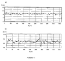
- the Raman spectra obtained by focused beam show the homogeneity of the graphene layer formed for films of dimensions of 1 ⁇ 1cm -2 .
- the electrical conductivity of the graphene films or of a few graphene layers depends on the nature of the substrate and the form of measure. On glass substrates (without metal layer) by measuring through a head of four tips measures between 500 and 10,000 Ohms/square are obtained. These values are significantly reduced when the measures of conductivity are carried out by depositing gold as contacts on the graphene layer and by measuring the conductivity through said contacts. On substrates that include the thin metal layer and measuring through gold contacts, resistances of between 10-20 Ohms/square are determined. In contrast, the precursor before being converted into graphene is shown as an insulator in any surface on which it is deposited.
- Example 1 Preparation of a graphene coating by carbonization of ammonium alginate on a glass surface.
- a solution of ammonium alginate is prepared by suspending commercial alginic acid (Sigma, CAS:9005-32-7, reference A7003-250G, 0.2 g) in 10 ml of Milli-Q H 2 O and adding a saturated solution of NH 4 OH until reaching a constant pH value equal to 8, thus achieving the solubilization of the polysaccharide.
- the resulting solution is filtered on a Nylon filter and is arranged in a spin coating apparatus.
- a 1 ⁇ 1 cm 2 piece of glass is extensively washed with isopropanol, Alconox detergent and finally with Milli-Q water.
- the glass is subjected to an ozonator for fifteen minutes before placing it in the spin coating apparatus.
- the formation of the film is carried out at 2000 rpm for fifty seconds.
- the film is left until it is dry and is introduced in an oven where it is heated to 200 °C for 2 hrs under a stream of argon saturated with water vapor. After that time the graphitization is carried out by gradual heating at 5 °C to 600 °C, maintaining this temperature for 6 hrs.
- the resulting sample is characterized by Raman spectroscopy, making several spectra in equally distributed points along the length and width of the surface. Standardization of the spectra reveals that the film is homogeneous and that it corresponds to a graphenic material. The thickness of this layer was determined by optical profilometry turning out to be 1 nm. X ray photoelectron spectroscopy indicates that the carbon present in the sample corresponds mostly to sp 2 carbons. The layer resistance of the resulting material turns out to be of 3,500 Ohms/square.
- Example 2 Preparation of a graphene coating doped with nitrogen by chitosan carbonization.
- aqueous solution is prepared by dissolution of commercial chitosan (Aldrich ref. 448869-50G, CAS:9012-76-4) in concentrated acetic acid (56 mg of chitosan in 0.225 ml of acetic acid) followed by dilution of this acetic solution in Milli-Q water (15 ml).
- the resulting aqueous solution is placed on the deposit of a spin coating apparatus and it is proceeded to the coating of a glass surface as indicated in Example 1.
- the graphitization method followed for the chitosan is also identical to that described in example 1.
- the sample of graphenic material obtained from the chitosan shows uniform Raman spectra throughout the whole surface and indistinguishable from those registered for the graphene sample obtained from alginate.
- the XPS spectrum reveals the presence of a 7% of N which corresponds with N sp2 and N sp2 with positive charge.
- the thickness of the film was 20 nm and the conductivity of the same was 4500 Ohms/square.
- Example 3 Preparation of a graphene coating from chitosan on a glass surface on which a nanometric layer of nickel metal has been deposited.
- the preparation of the glass substrate with a nanometric layer of nickel is carried out prior to the deposition of the chitosan layer in a steam deposition chamber of the metal by sublimation operating at a temperature of 1500 °C and a vacuum of 10 -5 mbar.
- the thickness of the nickel layer is controlled by the deposition time of the steam and turns out to be of 5 nm.
- the glass support coated with nickel has a transparency above 90%.
- a thin chitosan film is deposited operating with a solution such as the one described in example 2 and using a spin coating apparatus operating at 3000 rpm.
- the thickness of the resulting chitosan film is 2 nm and its conductivity is high and in any case greater than 1 MegaOhms/square.
- the substrate with the nanometric layers of nickel and chitosan is subjected to carbonization as described in example 2. Therefore graphene films on a transparent substrate with a high conductivity can be obtained without the need of proceeding to a stage of graphene transfer from one surface to another.
- the values of layer resistance obtained are 10-20 Ohms/square.
- Example 4 Preparation of a graphene coating from chitosan on a glass surface by microwave heating.
- a chitosan solution as the one shown in example 2 is prepared and it is proceeded to a coating of a clean glass substrate according to the method also described in example 2.
- the difference with example 2 is the carbonization method.
- the chitosan film is treated at 200 °C for 2 hrs in order to initiate a transformation of the chitosan derived from its partial dehydration. Then the material to be carbonized is transferred into a microwave oven and is heated up at a power of 1000 W for 20 min under inert atmosphere.
- Example 5 Preparation of a graphene coating doped with boron from a boronated derivative of ammonium alginate.
- the method of this example is identical to the one described in example 1, but using a boronated derivative of alginate in place of a commercial sample.
- This derivative is prepared in advance by reaction of a solution (5 ml) of sodium alginate (10 mg) with sodium borate (1 mg) at room temperature for 2 hrs. After this time, it is proceeded to the preparation of the coating by the spin coating apparatus, followed by carbonization at a temperature of 600 °C.
- Microscopy-EDX Analysis reveals the presence of boron as a doping agent for graphene in a percentage.
- the conductivity of the doped film is of 250 KiloOhms/square.
- Example 6 Preparation of a multilayer graphene coating each one with a different heteroatom.
- the present example consists of the preparation of a coating containing two graphene layers each one with a different heteroatom. For this, first it is proceeded to the embodiment of example 3. Next, on the resulting surface which already contains a graphene film arranged on a transparent glass with a nickel film, a layer of boronated ammonium alginate prepared as described in the example 5 is arranged and it is proceeded to its graphitization by thermal treatment. The final result is a substrate on which one thin nickel layer of 10 nm of thickness and two graphene layers are deposited, the first of which contains nitrogen in its composition and the second one contains boron.
- the 2 X 2 cm 2 square piece of quartz is immersed in a aqueous solution of 0.5 M hydrochloric acid. This treatment extends for a week at room temperature. After this time, the quartz piece is recovered, is washed with Milli-Q water and undergoes ozonation.
- the surface is left until it is dry in a clean environment and is thermally treated at 250 °C for 1 hr under a constant flow of nitrogen saturated with water vapor. After that time, the starch layer is graphitized at 850 °C for 5 hrs under nitrogen atmosphere, by gradual heating to 10 °C/min from 250 °C to 850 °C. The resulting material shows a conductivity of 1100 Ohms/square.
- Example 8 Preparation of a ceramics with graphene coating by carbonization of an ammonium alginate layer deposited on pressed ceramic precursor.
- a layer of a solution of ammonium alginate prepared as indicated in example 1 is deposited.
- the deposition is carried out conveniently by passing in a conveyor belt at a speed of 500 cm per minute a curtain of the solution containing ammonium alginate.
- the ceramic element is introduced into a bake furnace customary in ceramic installations and the pressed containing the alginate layer. It is heated at a temperature of 1200 °C for 1 hr in the total absence of oxygen.
- the data of Raman and X-ray photoelectron spectroscopy indicate the presence of the graphene in the surface of the ceramic element after the baking.
- the resistance of the surface was 1500 Ohms/square.
Landscapes
- Chemical & Material Sciences (AREA)
- Engineering & Computer Science (AREA)
- Nanotechnology (AREA)
- Materials Engineering (AREA)
- Organic Chemistry (AREA)
- Physics & Mathematics (AREA)
- Condensed Matter Physics & Semiconductors (AREA)
- General Physics & Mathematics (AREA)
- Crystallography & Structural Chemistry (AREA)
- Composite Materials (AREA)
- Inorganic Chemistry (AREA)
- Manufacturing & Machinery (AREA)
- Carbon And Carbon Compounds (AREA)
Applications Claiming Priority (2)
| Application Number | Priority Date | Filing Date | Title |
|---|---|---|---|
| ES201200100A ES2383356B1 (es) | 2012-02-06 | 2012-02-06 | Procedimiento para la preparación de películas de grafeno ó materiales grafénicos sobre sustratos no metálicos |
| PCT/ES2013/000026 WO2013117780A1 (es) | 2012-02-06 | 2013-02-05 | Procedimiento para la preparación de películas de grafeno ó materiales grafénicos sobre sustratos no metálicos |
Publications (2)
| Publication Number | Publication Date |
|---|---|
| EP2813469A1 true EP2813469A1 (de) | 2014-12-17 |
| EP2813469A4 EP2813469A4 (de) | 2015-09-16 |
Family
ID=46173009
Family Applications (1)
| Application Number | Title | Priority Date | Filing Date |
|---|---|---|---|
| EP13746795.7A Withdrawn EP2813469A4 (de) | 2012-02-06 | 2013-02-05 | Verfahren zur herstellung von filmen aus graphen oder graphenmaterialien auf nicht-metallischen substraten |
Country Status (9)
| Country | Link |
|---|---|
| US (1) | US9216435B2 (de) |
| EP (1) | EP2813469A4 (de) |
| CN (1) | CN104203814A (de) |
| CL (1) | CL2014002066A1 (de) |
| ES (1) | ES2383356B1 (de) |
| IN (1) | IN2014MN01654A (de) |
| MX (1) | MX2014009328A (de) |
| WO (1) | WO2013117780A1 (de) |
| ZA (1) | ZA201405836B (de) |
Cited By (3)
| Publication number | Priority date | Publication date | Assignee | Title |
|---|---|---|---|---|
| CN104759253A (zh) * | 2015-04-14 | 2015-07-08 | 中国广州分析测试中心 | 一种用于重金属富集或去除水中的污染物的石墨烯海绵及其制备方法 |
| KR20190085915A (ko) * | 2016-09-12 | 2019-07-19 | 더 유니버시티 오브 아델라이드 | 다목적 그래핀 기반 복합체 |
| ES2843743A1 (es) * | 2020-01-20 | 2021-07-20 | Primalchit Solutions S L | Esmalte anticorrosivo de material carbonoso, su procedimiento de obtencion y su uso |
Families Citing this family (9)
| Publication number | Priority date | Publication date | Assignee | Title |
|---|---|---|---|---|
| CN103626158B (zh) * | 2012-08-23 | 2016-04-06 | 中国科学院宁波材料技术与工程研究所 | 氮掺杂石墨烯的制备方法及其应用 |
| ES2471318B1 (es) * | 2012-11-22 | 2015-04-24 | Abengoa Solar New Technologies S.A. | Procedimiento de obtención de suspensiones o muestras sólidas de grafeno |
| CN103839695A (zh) * | 2012-11-23 | 2014-06-04 | 海洋王照明科技股份有限公司 | 石墨烯电极片及其制备方法和应用 |
| JP6201801B2 (ja) * | 2014-02-14 | 2017-09-27 | 株式会社デンソー | グラファイト薄膜の製造方法 |
| CN103803542B (zh) * | 2014-02-24 | 2016-01-20 | 南京理工大学 | 一种微生物燃料电池混合细菌氮掺杂石墨烯的制备方法 |
| CN103922328A (zh) * | 2014-04-18 | 2014-07-16 | 山东大学 | 一种利用壳聚糖制备含氮多级孔三维石墨烯的方法 |
| CN108472665A (zh) * | 2015-11-12 | 2018-08-31 | 康奈尔大学 | 空气控制的电喷雾制造及其产品 |
| US11628416B2 (en) * | 2017-07-11 | 2023-04-18 | Edwin SAFARI | Graphene coated glass material and uses thereof |
| CN113024278A (zh) * | 2021-03-04 | 2021-06-25 | 四川大学 | 一种具有原位石墨烯膜的磷酸钙陶瓷及其制备方法和应用 |
Family Cites Families (3)
| Publication number | Priority date | Publication date | Assignee | Title |
|---|---|---|---|---|
| CA2149853A1 (en) * | 1995-05-19 | 1996-11-20 | Jiayu Simon Xue | Pre-graphitic carbonaceous insertion compounds and use as anodes in rechargeable batteries |
| EP2456716A2 (de) * | 2009-07-22 | 2012-05-30 | Wisys Technology Foundation, Inc. | Kohlenstoff-mikrokügelchen mit hierarchischer struktur |
| KR101622304B1 (ko) | 2009-08-05 | 2016-05-19 | 삼성전자주식회사 | 그라펜 기재 및 그의 제조방법 |
-
2012
- 2012-02-06 ES ES201200100A patent/ES2383356B1/es not_active Expired - Fee Related
-
2013
- 2013-02-04 US US13/758,415 patent/US9216435B2/en not_active Expired - Fee Related
- 2013-02-05 MX MX2014009328A patent/MX2014009328A/es unknown
- 2013-02-05 CN CN201380008199.6A patent/CN104203814A/zh active Pending
- 2013-02-05 WO PCT/ES2013/000026 patent/WO2013117780A1/es not_active Ceased
- 2013-02-05 IN IN1654MUN2014 patent/IN2014MN01654A/en unknown
- 2013-02-05 EP EP13746795.7A patent/EP2813469A4/de not_active Withdrawn
-
2014
- 2014-08-04 CL CL2014002066A patent/CL2014002066A1/es unknown
- 2014-08-08 ZA ZA2014/05836A patent/ZA201405836B/en unknown
Cited By (6)
| Publication number | Priority date | Publication date | Assignee | Title |
|---|---|---|---|---|
| CN104759253A (zh) * | 2015-04-14 | 2015-07-08 | 中国广州分析测试中心 | 一种用于重金属富集或去除水中的污染物的石墨烯海绵及其制备方法 |
| CN104759253B (zh) * | 2015-04-14 | 2017-10-20 | 中国广州分析测试中心 | 一种用于重金属富集或去除水中的污染物的石墨烯海绵及其制备方法 |
| KR20190085915A (ko) * | 2016-09-12 | 2019-07-19 | 더 유니버시티 오브 아델라이드 | 다목적 그래핀 기반 복합체 |
| ES2843743A1 (es) * | 2020-01-20 | 2021-07-20 | Primalchit Solutions S L | Esmalte anticorrosivo de material carbonoso, su procedimiento de obtencion y su uso |
| WO2021148695A1 (es) * | 2020-01-20 | 2021-07-29 | Primalchit Solutions, S.L. | Esmalte anticorrosivo de material carbonoso, su procedimiento de obtención y su uso |
| EP4095112A4 (de) * | 2020-01-20 | 2023-09-27 | Primalchit Solutions, S.L. | Korrosionsschutzemaille mit kohlenstoffmaterial, verfahren zu seiner herstellung und seine verwendung |
Also Published As
| Publication number | Publication date |
|---|---|
| WO2013117780A1 (es) | 2013-08-15 |
| US20130209793A1 (en) | 2013-08-15 |
| MX2014009328A (es) | 2015-02-24 |
| US9216435B2 (en) | 2015-12-22 |
| ES2383356B1 (es) | 2013-04-04 |
| IN2014MN01654A (de) | 2015-05-29 |
| ES2383356A1 (es) | 2012-06-20 |
| ZA201405836B (en) | 2015-10-28 |
| CL2014002066A1 (es) | 2015-03-13 |
| CN104203814A (zh) | 2014-12-10 |
| EP2813469A4 (de) | 2015-09-16 |
Similar Documents
| Publication | Publication Date | Title |
|---|---|---|
| US9216435B2 (en) | Method for the preparation of graphene or graphenic materials films on non-metal substrates | |
| Primo et al. | From biomass wastes to large-area, high-quality, N-doped graphene: catalyst-free carbonization of chitosan coatings on arbitrary substrates | |
| Zheng et al. | Improved electrical and optical characteristics of transparent graphene thin films produced by acid and doping treatments | |
| Silva Filho et al. | Perovskite thin film synthesised from sputtered lead sulphide | |
| JP5483228B2 (ja) | 導電性ダイヤモンド中空ファイバー膜及び導電性ダイヤモンド中空ファイバー膜の製造方法 | |
| JP5578640B2 (ja) | 導電性膜、導電性基板、透明導電性フィルムおよびこれらの製造方法 | |
| KR20170020533A (ko) | 그래핀으로 코팅된 코어-쉘 구조를 가지는 금속 나노와이어 및 이의 제조방법 | |
| JP2013513544A (ja) | 基材へのグラフェンの広範囲析出およびそれを含む製品 | |
| Shi et al. | Fabrication of transparent, flexible conducing graphene thin films via soft transfer printing method | |
| KR20200121674A (ko) | 맥신 박막의 제조방법 및 이로부터 제조된 맥신 박막 | |
| Kanishka et al. | Rapid and scalable fabrication of reduced graphene oxide conducting films by ethanol-assisted thermal annealing of graphene oxide | |
| Ruan et al. | Lightwave irradiation-assisted low-temperature solution synthesis of indium-tin-oxide transparent conductive films | |
| Colak et al. | Effect of consumption of the sol–gel deposited ZnO seed layer on the growth and properties of high quality ZnO nanorods | |
| Muhl et al. | Transparent conductive carbon nanotube films | |
| Lee et al. | A Sweeter Solution: Caramelized Sucrose Additives Render Eco‐Friendly and High‐Performance Perovskite Solar Cells | |
| Jeong et al. | One‐Step Transfer and Integration of Multifunctionality in CVD Graphene by TiO2/Graphene Oxide Hybrid Layer | |
| Lock et al. | Dry graphene transfer print to polystyrene and ultra-high molecular weight polyethylene− Detailed chemical, structural, morphological and electrical characterization | |
| KR101484850B1 (ko) | 2차원 판상 구조 탄소 소재와 그 제조 방법 | |
| Peiris et al. | Aerosol-assisted fabrication of tin-doped indium oxide ceramic thin films from nanoparticle suspensions | |
| Qiu et al. | ILGAR CuInS2 films from various preparation conditions | |
| Tong et al. | Growth of ZnO nanorod arrays on flexible substrates: effect of precursor solution concentration | |
| John et al. | Optoelectronic Characteristics of In2S3-CNT Nanocomposite Thin Films for Photodetector Application: John, Sebastian, Cyriac, Paul, Jose, Shaji, and Augustine | |
| Shenoy et al. | Substrate dependent photochemical oxidation of monolayer graphene | |
| Kutlu-Narin et al. | Investigation of Structural and Optical Properties of ZnO Thin Films Grown on Different Substrates by Mist‐CVD Enhanced with Ozone Gas Produced by Corona Discharge Plasma | |
| Gunasekaran et al. | Modulation of ZnO film thickness and formation of water-hyacinth nanostructure |
Legal Events
| Date | Code | Title | Description |
|---|---|---|---|
| PUAI | Public reference made under article 153(3) epc to a published international application that has entered the european phase |
Free format text: ORIGINAL CODE: 0009012 |
|
| 17P | Request for examination filed |
Effective date: 20140904 |
|
| AK | Designated contracting states |
Kind code of ref document: A1 Designated state(s): AL AT BE BG CH CY CZ DE DK EE ES FI FR GB GR HR HU IE IS IT LI LT LU LV MC MK MT NL NO PL PT RO RS SE SI SK SM TR |
|
| AX | Request for extension of the european patent |
Extension state: BA ME |
|
| DAX | Request for extension of the european patent (deleted) | ||
| RA4 | Supplementary search report drawn up and despatched (corrected) |
Effective date: 20150818 |
|
| RIC1 | Information provided on ipc code assigned before grant |
Ipc: B82Y 30/00 20110101ALI20150812BHEP Ipc: B82Y 40/00 20110101ALI20150812BHEP Ipc: C01B 31/02 20060101AFI20150812BHEP Ipc: C01B 31/04 20060101ALI20150812BHEP Ipc: H01B 1/04 20060101ALI20150812BHEP |
|
| STAA | Information on the status of an ep patent application or granted ep patent |
Free format text: STATUS: THE APPLICATION IS DEEMED TO BE WITHDRAWN |
|
| 18D | Application deemed to be withdrawn |
Effective date: 20160901 |