EP2814182A2 - Procédé de réduction de distorsion de deuxième ordre dans un mélangeur à rejet d'harmonique - Google Patents
Procédé de réduction de distorsion de deuxième ordre dans un mélangeur à rejet d'harmonique Download PDFInfo
- Publication number
- EP2814182A2 EP2814182A2 EP14171845.2A EP14171845A EP2814182A2 EP 2814182 A2 EP2814182 A2 EP 2814182A2 EP 14171845 A EP14171845 A EP 14171845A EP 2814182 A2 EP2814182 A2 EP 2814182A2
- Authority
- EP
- European Patent Office
- Prior art keywords
- signal
- mixing means
- converted
- mixer
- phase
- Prior art date
- Legal status (The legal status is an assumption and is not a legal conclusion. Google has not performed a legal analysis and makes no representation as to the accuracy of the status listed.)
- Granted
Links
Images


Classifications
-
- H—ELECTRICITY
- H04—ELECTRIC COMMUNICATION TECHNIQUE
- H04B—TRANSMISSION
- H04B1/00—Details of transmission systems, not covered by a single one of groups H04B3/00 - H04B13/00; Details of transmission systems not characterised by the medium used for transmission
- H04B1/06—Receivers
- H04B1/10—Means associated with receiver for limiting or suppressing noise or interference
-
- H—ELECTRICITY
- H04—ELECTRIC COMMUNICATION TECHNIQUE
- H04B—TRANSMISSION
- H04B1/00—Details of transmission systems, not covered by a single one of groups H04B3/00 - H04B13/00; Details of transmission systems not characterised by the medium used for transmission
- H04B1/06—Receivers
- H04B1/16—Circuits
- H04B1/30—Circuits for homodyne or synchrodyne receivers
-
- H—ELECTRICITY
- H03—ELECTRONIC CIRCUITRY
- H03D—DEMODULATION OR TRANSFERENCE OF MODULATION FROM ONE CARRIER TO ANOTHER
- H03D7/00—Transference of modulation from one carrier to another, e.g. frequency-changing
- H03D7/14—Balanced arrangements
Definitions
- the present invention relates generally to a harmonic rejection mixer, and more specifically, to a method for reducing second order intermodulation distortion in a harmonic rejection mixer.
- SDR Software-Defined Radio
- Most SDR receivers use a direct conversion architecture to obtain high integration.
- Telecommunication standards such as GSM, WCDMA, LTE, WLAN etc., define in their specifications strict requirements for suppression of undesired signals.
- SAW Surface Acoustic Wave
- To comply with the requirements a Surface Acoustic Wave (SAW) filter is used for each supported standard.
- BoM Bill-of-Material
- the SAW filters are removed. This causes problems that detrimentally affect the receiver performance.
- a direct-conversion receiver lacking a SAW filter requires more stringent constraints on some of the non-idealities of its analog circuitry, affecting the overall receiver performance.
- a signal transmitted by the transmitter leaking into the front-end path of the receiver can detrimentally affect its performance.
- a signal transmitted by the transmitter leaking into the front-end path of the receiver can detrimentally affect its performance.
- non-linearity problems arise due to the considerably reduced attenuation of the leaked transmitted frequency into the receiver path.
- the receiver sensitivity is degraded by the second order intermodulation distortion (IMD2) caused by its non-linear elements.
- IMD2 intermodulation distortion
- every signal, even the desired signal, entering a non-linear element gives rise to distortion products by generating a signal centred at zero frequency (DC frequency).
- a highly linear receiver is thus required to prevent generating distortion products at baseband frequency.
- the second order intercept point (IP2) is a measure of the second order non-linearity of the receiver and helps quantifying the input level at which the power of second order intermodulation distortion (IMD2) products at baseband frequency equals the power of the desired signal.
- IMD2 second order intermodulation distortion
- Major sources of non-linearity affecting the IP2 performance of a receiver include transistor mismatch and layout asymmetry in the mixer. Thus, without a high IP2 of the mixer, the receiver sensitivity is greatly reduced.
- the present disclosure aims at providing a method for reducing second order intermodulation distortion in a harmonic rejection mixer.
- the present disclosure relates to a method for reducing second order intermodulation distortion in a harmonic rejection mixer comprising a plurality of mixing means.
- the method comprises
- the I- and Q-baseband signals are each reconstructed by recombining three mixer outputs.
- the proposed method allows reducing IMD2 in the reconstructed I- and Q- baseband signals at the harmonic rejection mixer output by calibrating only one mixer in each I- and Q-channel. This allows only one calibration circuitry to be used for calibrating a harmonic rejection mixer.
- the calibration method can as well be applied to a conventional four-phase mixer, thus reusing the same calibration circuitry.
- the reconstruction dependencies are avoided by calibrating the down-converted component not affecting the reconstruction of the respective baseband signal, the reduction of the second order intermodulation distortion in each of the I- and Q- baseband signal can be done separately.
- the mixer of which the output is applied to a zero gain amplifier is calibrated.
- IP2 calibration of the I-baseband signal can be performed, followed by IP2 calibration of the Q-baseband signal, or vice versa.
- a local oscillator signal of the plurality of local oscillator signals is used with a phase of zero degrees and in the second mixing means a local oscillator signal of said plurality with a phase of ninety degrees.
- compensating the transistor mismatch involves changing a transistor output current in the first or the second mixing means.
- each mixer may be a differential mixer.
- the goal of the method is to equalize the IMD2 in the positive and negative components of the reconstructed I- or Q-differential baseband signals. This allows the method to achieve a cost efficient and time saving IMD2 reduction.
- the method according to the invention is advantageously applied in a wireless device comprising such a harmonic rejection mixer.
- the method allows further improving the linearity of a wireless device and thus minimizing the second order intermodulation distortion of the wireless device.
- This method allows removing the area expensive SAW filter used for suppressing a large amplitude modulated blocker signal close to the desired signal to achieve sufficient output SNR without IP2 calibration in the wireless device. Removing the SAW filter also allows a wider operating bandwidth of the receiver.
- this method allows using a conventional IP calibration circuitry in a wireless device with a harmonic rejection mixer.
- the present disclosure relates to harmonic rejection mixer adapted for reducing second order intermodulation distortion, said harmonic rejection mixer arranged for receiving a radio frequency signal and comprising
- the calibration circuitry comprises a digital-to-analog converter, DAC, and control means to control said DAC.
- each mixing means of the harmonic rejection mixer is differential.
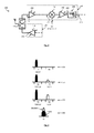
- Fig.1 illustrates a conventional FDD radio system employing a band-pass filter and a harmonic rejection mixer.
- Fig.2 illustrates, in the conventional FDD radio system of Fig.1 , the signals at the output of the transmitter, at the input of the receiver, at the input of the harmonic rejection mixer and at the output of the receiver front-end, respectively.
- Fig.3 illustrates an FDD radio system of Fig.1 without a band-pass filter.
- Fig.4 illustrates, in the FDD radio system of Fig.3 , the signals at the output of the transmitter, at the input of the receiver, at the input of the harmonic rejection mixer and at the output of the receiver front-end, respectively.
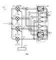
- Fig.5 illustrates a differential harmonic rejection mixer according to an exemplary embodiment.
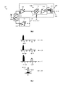
- Fig.6 illustrates an FDD radio system of Fig.3 employing a harmonic rejection mixer according to an exemplary embodiment.
- Fig.7 illustrates, in the FDD radio system of Fig.6 , the signals at the output of the transmitter, at the input of the receiver, at the input of the harmonic rejection mixer and at the output of the receiver front-end, respectively.
- Fig.8 illustrates a wireless device with a receiver having a harmonic rejection mixer and a four-phase mixer.
- Fig.1 illustrating a front-end chain of an example FDD radio system 100, comprising a transmitter 120 and a receiver 140.
- the transmitter front-end section is shown to comprise a power amplifier 130 and a duplexer 110, other analog circuitry is omitted for simplicity.
- the receiver front-end section comprises a duplexer 110, at least one Low Noise Amplifier (LNA) 150 and a band-pass SAW filter 160.
- LNA Low Noise Amplifier
- SAW filter 160 band-pass SAW filter
- the mixer 170 down-converts the filtered signal 171 to baseband (DC) frequency with a plurality local oscillators signals LO, thus generating a plurality of down-converted signals.
- the down-converted signals are amplified by a variable gain amplifier 180, combined by an adder 190 (not shown as a block in the figure) to output the reconstructed baseband signal.
- the baseband is filtered by a low-pass filter 200.
- Fig.2 illustrates the transmitter output signal 131, the LNA input signal 151, the mixer input signal 171 and the output signal 141 of the receiver front-end, respectively, for the FDD system of Fig.1 .
- the LNA input signal 151 comprises transmitter leakage (TX leakage) and the received signal (the desired signal).
- the SAW filter attenuates undesired signals (e.g. out-of-band signals).
- the SAW filter suppresses a leakage signal leaked from the transmitter into the receiver through the duplexer.
- the use of a SAW filter guarantees a low IMD2 product at the receiver front-end output.
- the generated IMD2 product is small with respect to the desired signal and thus does not degrade the signal-to-noise ratio (SNR) at the receiver.
- SNR signal-to-noise ratio
- Fig.3 shows an example FDD radio system without SAW filter in the receiver.
- Fig.4 shows the respective signals of the radio system of Fig.3 at the LNA input 151, at the mixer input 171 and at the receiver front-end output 141.
- the unwanted signals i.e. the TX leakage
- the IMD2 component at DC frequency is much bigger (see signal 141 in Fig.4 ). This leads to a poor SNR and, thus, makes it difficult to meet the required receiver sensitivity.
- IP2 second order intercept point
- a mixer is a non-linear circuit essentially comprising of transistors.
- a differential Gilbert-cell mixer transistor mismatch causes the signal at its differential output to be different.
- the greater the transistor mismatch in the mixer the greater the difference between the differential output signals and the lower the IP2.
- the differential output signals are matched, i.e. the difference between the positive and negative baseband signal is zero.
- the IMD2 can reduce the receiver sensitivity.
- IP2 second order intercept point
- the transistor mismatch of a mixer needs to be calibrated/reduced.
- a harmonic rejection mixer is commonly used for cancellation of, for example, third, fifth and higher order harmonics.
- Such mixers are widely used e.g. in television receivers, but recently they have been frequently applied in wireless devices as well.
- a harmonic rejection mixer In order to deal with 3 rd and 5 th order harmonics a harmonic rejection mixer often uses eight phases. However, depending on the order of the harmonics to be suppressed, the harmonic rejection mixer can be extended to use a greater number of phases, for example, 12 phases, 16 phases and so on. Any number 4N of phases can be envisaged, with N representing an integer value.
- Fig.5 shows an embodiment of the present invention : a harmonic rejection mixer 1700 comprising a plurality of mixers 1701-1704 multiplying a radio frequency signal 171 with a plurality of local oscillator signals LO1-LO4 phase shifted with respect to each other. Each mixer outputs a down-converted signal 1721-1724 having a phase shift determined by the phase shift of the respective LO signal. Amplifiers 180 amplify each down-converted signal with an amplification factor depending on its phase shift. The amplified signals are then combined together by the adder 190 to produce the in-phase component I BB and quadrature component Q BB of the baseband signal.
- the in-phase component I BB and the quadrature component Q BB are in the art also called the baseband 0 degrees and baseband 90 degrees component.
- a differential HRM mixer designed for cancelling 3 rd and 5 th harmonics uses 8 phases with an incremental phase step of 45°, i.e. 0°, 45°, 90°, 135°, 180°, 225°, 270° and 315° phase.
- the 3 rd and 5 th harmonics in the reconstructed in-phase baseband signal I BB are cancelled by amplifying down-converted signals with phases rotated over 45°, 90° and 135° with an appropriate amplification factor, for example 1/ ⁇ 2, 1 and 1/ ⁇ 2, and then summing them together.
- an appropriate amplification factor for example 1/ ⁇ 2, 1 and 1/ ⁇ 2, and then summing them together.
- the quadrature baseband signal Q BB this is achieved by summing down-converted signals with phases rotated over 0°, 45° and 135° after their amplification with amplification factors -1, -1/ ⁇ 2 and 1/ ⁇ 2.
- the differential phases i.e. 180°, 225°, 270° and 315°.
- no HR3 or HR5 frequency components are generated in the baseband signal output at the HRM mixer.
- calibrating the mixers has an impact on the IMD2 product on both I- and Q-baseband signals. This additionally complicates the IP2 calibration of the harmonic rejection mixer as convergence (i.e. reaching a minimum point) is difficult to achieve. Calibration is performed in an iterative manner (i.e. at each iteration different mixer(s) need to be calibrated and the IMD2 at both I- and Q-baseband signal components needs to be measured).
- the IMD2 in the in-phase or quadrature baseband signal can be reduced or even eliminated by calibrating one mixer that does not contribute to the reconstruction of the in-phase baseband signal and one mixer that does not contribute to the reconstruction of the quadrature baseband signal.
- the IMD2 product caused by the overall mismatch contributed by the mixers (e.g. 1702,1703,1704) involved in the reconstruction of one of the baseband signal component (e.g. I BB ) is reduced or even eliminated by calibrating a mixer that does not contribute to the reconstruction of the other baseband signal component (e.g. Q BB ).
- the calibrated mixer is not affecting the reconstruction of the other baseband signal component, i.e.
- IP2 the interdependence between the IP2 calibration of the in-phase and quadrature baseband signal is eliminated.
- IP2 second order intercept point
- Adjusting transistor mismatch can be achieved by conventional mismatch calibrating techniques, for example, by changing transistor gate voltage, mixer common mode voltage or current injection. Each of these calibration techniques changes the output current of the transistor(s) in a mixer. Other transistor parameters could also be adjusted to correct for the IP2 with the method of the present disclosure.
- the effect of adjusting the transistor mismatch is an offset adjustment of the signals outputted by the mixer.
- the present disclosure proposes a method for reducing second order intermodulation distortion (IMD2) in the reconstructed baseband signal at the output of the harmonic rejection mixer, the reconstructed baseband signal comprising an in-phase component I BB and a quadrature component Q BB .
- IMD2 second order intermodulation distortion
- the method proposes compensating a transistor mismatch in a first mixer 1701 to reduce the IMD2 product in the quadrature component Q BB , by adjusting the output current of the first mixer and calibrating a second mixer 1703 to reduce the IMD2 product in the in-phase baseband signal I BB by adjusting its output current.
- the output current of the mixers can be adjusted by adjusting the output current of at least one of its transistors using any conventional technique as described above.
- the output current of the transistor(s) in the first mixer 1701 and in the second mixer 1703 is adjusted to a certain value guaranteeing a sufficiently low IMD2 product in the respective Q- and I-baseband signal.
- the value of the IMD2 product in the in-phase and the quadrature component may be different, however both values should meet the IP2 requirements set by the telecommunication standard such as GSM, WCDMA, LTE, WLAN etc.
- the output current of the transistor(s) in the first mixer 1701 may be adjusted until a minimum of the IMD2 product in the quadrature component of the baseband signal is reached.
- the output current of the transistor(s) in the second mixer 1703 may be adjusted until a minimum of the IMD2 product in the in-phase baseband signal is reached.
- the calibration circuitry 210 arranged for calibrating the first and the second mixer is designed to provide for a sufficient range of mismatch compensation, i.e. to provide a sufficient range for adjusting e.g. the output current of the transistor(s), so that the IMD2 product in the baseband signal may be reduced to meet the IP2 requirements set by the telecommunication standard. This range depends on the mismatch in each mixer and the scaling factors (amplification factors) applied on signals at the output of the mixers - down-converted signals 1721-1724.
- the calibration circuitry may be realized by a digital-to-analog converter (DAC) and a control logic circuit.
- the control logic circuit controls the operation of the DAC based on detected changes in the IMD2.
- the signal at the output of the DAC controls the output current of the transistor(s), for example by modifying the voltage applied at the transistor bias.
- a software program may be used to control the operation of the DAC.
- the first mixer 1701 and the second mixer 1703 being calibrated are chosen to allow for independent IP2 calibration of the in-phase and quadrature baseband signals, by calibrating for the I- and Q-baseband components a single mixer that does not contribute to the reconstruction of the baseband component in question - the output of that mixer is weighted with zero gain when performing the reconstruction.
- the down-converted signal 1721 at the output of the first mixer 1701 is amplified with a factor of zero before combining it with the other down-converted signals 1722-1724 to produce the in-phase signal I BB .
- the down-converted signal 1723 at the output of the second mixer 1703 is amplified with a factor of zero before combining it with the other down-converted signals 1721,1722,1724 to produce the quadrature signal Q BB .
- the IMD2 of I BB may be reduced independently from the IMD2 of Q BB , and vice versa.
- this allows the IP2 calibration to be achieved by calibrating only two mixers, and hence only two calibration circuits are required as, for example, for the calibration of a conventional four-phase mixer. This greatly simplifies the circuit design, the area footprint and the overall power consumption of the radio device.
- each individual mixer 1701 - 1704 of the harmonic rejection mixer may be a differential mixer.
- each mixer outputs a differential down-converted signal and the reconstructed baseband signal components (i.e. I BB and Q BB ) are also differential.
- Using differential mixers helps reducing more effectively the second order distortion, as for the calibration it is only required to equalize the IMD2 products in each respective differential output of the harmonic rejection mixer 170. For example, the IMD2 is reduced or even completely eliminated when the corresponding IMD2 products in the differential signals I BB + and I BB - are close to one another or even completely cancel each other.
- Equations (1) and (2) show the contribution of each individual mixer to the overall IMD2 product for each baseband signal component, respectively. These expressions have to be reduced as much as possible.
- each mixer contributes an amount A and B to the overall IMD2 of the respective baseband signal component.
- A1 and B1 are the amounts of IMD2 generated by the first mixer 1701 at its respective differential outputs
- A2 and B2 are the IMD2 amount generated by the mixer 1702 and so on.
- the IMD2 for the I-component of the baseband signal is reduced by calibrating the second mixer 1703. Adjusting the output current of the transistor(s) of the second mixer changes coefficients k1 and k2 and, thus, the amount of the IMD2 at the differential output of the mixer 1703.
- IP2 calibration of I BB is achieved when both k1 and k2 coefficients reach a value such that the resulting IMD2 in the differential I BB + and I BB - baseband signals are equalized and hence IMD2 I BB is equal to zero.
- IP2 calibration of the second baseband signal I BB is achieved when the n1 and n2 coefficients reach a value such that the resulting IMD2 in the differential Q BB + and Q BB - baseband signals are equalized and hence IMD2 Q BB is equal to zero. This allows a cost efficient and time saving calibration.
- Fig.6 shows an FDD radio system 100 comprising the harmonic rejection mixer 1700 of Fig.5 , with four differential mixers 1701-1704, illustrated as a single mixer 170. Each of these mixers is arranged to multiply the signal at its respective input with a pair of LO signals each having a different phase.
- the down-converted signals at the outputs of the four mixers are first amplified by amplifiers 180 and then combined by the adder 190 to realize the harmonic rejection mixing of I-channel and Q-channel baseband signal.
- the mixer 170 receives a local oscillator signal with 8 different phases with an incremental step of 45° (LO 0°:45°:315°).
- the adder 190 combining the down-converted signals to produce the I- and Q- baseband signals is not illustrated as a block, but only its location is indicated.
- Fig.7 shows signals of the radio system of Fig.6 at the input of the LNA 151, at the input of the harmonic rejection mixer 171 and at the output of the front-end of the receiver 141, respectively.
- the unwanted signals are sufficiently suppressed and the IMD2 component at baseband frequency is sufficiently lowered (see 141 in Fig.4 ) to meet the IP2 requirements for the receiver as set by the telecommunication standards.
- the method guarantees a high signal-to-noise ratio (SNR) as well as the required receiver sensitivity.
- SNR signal-to-noise ratio
- the method may be used for reducing second order intermodulation distortion (IMD2) in a wireless device.
- Fig.8 shows an example of a wireless device comprising a harmonic rejection mixer 1700 realized by mixer 170 together with the amplifiers 180 and the adder 190 (only its location in the device is illustrated).
- the wireless device may as well comprise a conventional four-phase mixer 220.
- the proposed method can be applied for calibrating both the harmonic rejection mixer 1700 and the conventional mixer 220 of the radio device of Fig.8 and achieve an IP2 high enough to guarantee a receiver sensitivity in accordance with the telecommunication standards (e.g. GSM, WCDMA, LTE, WLAN, etc.).
- the method of the present disclosure offers a number of advantages. It reduces the required amount of calibration circuitry. For a harmonic rejection mixer designed for third and fifth order harmonics cancellation, only two calibration circuitry are required. In this case it is sufficient to calibrate only 2 mixers, instead of all four. In case of a HRM designed for cancellation of even higher harmonics, again only 2 mixers need to be calibrated, instead of 6 or more.
- the calibration technique offers low complexity, as the overall mismatch of each I- and Q- channel (i.e. the mismatch of each mixer contributing to the reconstruction of the respective baseband signal components) is calibrated independently of the other. This allows each quadrature channel to be calibrated, separately.
- a computer program may be stored/distributed on a suitable medium, such as an optical storage medium or a solid-state medium supplied together with or as part of other hardware, but may also be distributed in other forms, such as via the Internet or other wired or wireless telecommunication systems. Any reference signs in the claims should not be construed as limiting the scope.
Landscapes
- Engineering & Computer Science (AREA)
- Computer Networks & Wireless Communication (AREA)
- Signal Processing (AREA)
- Power Engineering (AREA)
- Transmitters (AREA)
- Superheterodyne Receivers (AREA)
Priority Applications (1)
| Application Number | Priority Date | Filing Date | Title |
|---|---|---|---|
| EP14171845.2A EP2814182B1 (fr) | 2013-06-10 | 2014-06-10 | Procédé de réduction de distorsion de deuxième ordre dans un mélangeur à rejet d'harmonique |
Applications Claiming Priority (2)
| Application Number | Priority Date | Filing Date | Title |
|---|---|---|---|
| EP13171264 | 2013-06-10 | ||
| EP14171845.2A EP2814182B1 (fr) | 2013-06-10 | 2014-06-10 | Procédé de réduction de distorsion de deuxième ordre dans un mélangeur à rejet d'harmonique |
Publications (3)
| Publication Number | Publication Date |
|---|---|
| EP2814182A2 true EP2814182A2 (fr) | 2014-12-17 |
| EP2814182A3 EP2814182A3 (fr) | 2014-12-31 |
| EP2814182B1 EP2814182B1 (fr) | 2017-09-13 |
Family
ID=48607118
Family Applications (1)
| Application Number | Title | Priority Date | Filing Date |
|---|---|---|---|
| EP14171845.2A Active EP2814182B1 (fr) | 2013-06-10 | 2014-06-10 | Procédé de réduction de distorsion de deuxième ordre dans un mélangeur à rejet d'harmonique |
Country Status (3)
| Country | Link |
|---|---|
| US (1) | US9325358B2 (fr) |
| EP (1) | EP2814182B1 (fr) |
| JP (1) | JP6491426B2 (fr) |
Families Citing this family (11)
| Publication number | Priority date | Publication date | Assignee | Title |
|---|---|---|---|---|
| US9088471B1 (en) * | 2014-02-19 | 2015-07-21 | Qualcomm Incorporated | Quadrature combining and adjusting |
| US10171034B2 (en) | 2016-04-08 | 2019-01-01 | Mediatek Inc. | Phase-rotated harmonic-rejection mixer apparatus |
| US10419046B2 (en) | 2016-05-26 | 2019-09-17 | Mediatek Singapore Pte. Ltd | Quadrature transmitter, wireless communication unit, and method for spur suppression |
| US10009050B2 (en) * | 2016-05-26 | 2018-06-26 | Mediatek Singapore Pte. Ltd. | Quadrature transmitter, wireless communication unit, and method for spur suppression |
| US10523250B2 (en) * | 2016-09-06 | 2019-12-31 | Apple Inc. | Systems and methods for mitigating intermodulation effects |
| US11923884B2 (en) * | 2021-09-24 | 2024-03-05 | Qualcomm Incorporated | Configurable harmonic rejection mixer (HRM) |
| DE102022108428A1 (de) * | 2022-04-07 | 2023-10-12 | Infineon Technologies Ag | Radarvorrichtung mit kompensation von nichtlinearitäten |
| US12494809B2 (en) * | 2022-09-13 | 2025-12-09 | Qualcomm Incorporated | Mixer with bias sharing |
| US20240106474A1 (en) * | 2022-09-22 | 2024-03-28 | Qualcomm Incorporated | Mixer second-order input intercept point (iip2) calibration using a single tone generator and/or reverse feedthrough |
| US12537535B2 (en) * | 2022-09-22 | 2026-01-27 | Qualcomm Incorporated | Symmetrical resistive harmonic rejection mixer (HRM) |
| US12375324B2 (en) | 2023-11-09 | 2025-07-29 | Gregory A. Dockery | Electrical current balancing system |
Family Cites Families (8)
| Publication number | Priority date | Publication date | Assignee | Title |
|---|---|---|---|---|
| US7130604B1 (en) * | 2002-06-06 | 2006-10-31 | National Semiconductor Corporation | Harmonic rejection mixer and method of operation |
| EP1726099A1 (fr) * | 2004-03-02 | 2006-11-29 | Koninklijke Philips Electronics N.V. | Serialisation de codage de sequences multibandes pour une architecture de recepteur a bande ultralarge presentant une complexite et une consommation d'energie reduites |
| JP2006054547A (ja) * | 2004-08-10 | 2006-02-23 | Renesas Technology Corp | 受信装置および受信特性の最適化方法 |
| JP4541800B2 (ja) * | 2004-08-20 | 2010-09-08 | ルネサスエレクトロニクス株式会社 | インダクタを備えた半導体装置 |
| US8149955B2 (en) * | 2008-06-30 | 2012-04-03 | Telefonaktiebolaget L M Ericsson (Publ) | Single ended multiband feedback linearized RF amplifier and mixer with DC-offset and IM2 suppression feedback loop |
| US8060043B2 (en) * | 2008-10-09 | 2011-11-15 | Freescale Semiconductor | Adaptive IIP2 calibration |
| EP2246975B1 (fr) | 2009-04-28 | 2014-02-26 | Nxp B.V. | Étalonnage de mélangeur harmonique-rejet passif |
| US8838057B2 (en) * | 2011-04-04 | 2014-09-16 | Maxlinear, Inc. | Harmonic rejection mixer architecture with reduced sensitivity to gain and phase mismatches |
-
2014
- 2014-06-10 US US14/300,574 patent/US9325358B2/en active Active
- 2014-06-10 JP JP2014119286A patent/JP6491426B2/ja active Active
- 2014-06-10 EP EP14171845.2A patent/EP2814182B1/fr active Active
Non-Patent Citations (1)
| Title |
|---|
| None |
Also Published As
| Publication number | Publication date |
|---|---|
| JP6491426B2 (ja) | 2019-03-27 |
| EP2814182A3 (fr) | 2014-12-31 |
| JP2014239440A (ja) | 2014-12-18 |
| US9325358B2 (en) | 2016-04-26 |
| EP2814182B1 (fr) | 2017-09-13 |
| US20140364076A1 (en) | 2014-12-11 |
Similar Documents
| Publication | Publication Date | Title |
|---|---|---|
| EP2814182B1 (fr) | Procédé de réduction de distorsion de deuxième ordre dans un mélangeur à rejet d'harmonique | |
| US8411730B2 (en) | Semiconductor integrated communication circuit and operation method thereof | |
| CA2474502C (fr) | Etalonnage de reduction de distorsion | |
| US8233871B2 (en) | Incompressible RF receiver | |
| EP2432131B1 (fr) | Systèmes et procédés d'annulation d'émission de parasites | |
| EP2169837B1 (fr) | Technique pour supprimer le bruit dans un dispositif de transmetteur | |
| CN107437959B (zh) | 正交发射机,无线通信单元以及发射机中处理信号的方法 | |
| US7783273B2 (en) | Method and system for calibrating frequencies-amplitude and phase mismatch in a receiver | |
| US8149955B2 (en) | Single ended multiband feedback linearized RF amplifier and mixer with DC-offset and IM2 suppression feedback loop | |
| US10419046B2 (en) | Quadrature transmitter, wireless communication unit, and method for spur suppression | |
| US7003263B2 (en) | Telecommunications receiver and a transmitter | |
| US8805304B2 (en) | Linearization of broadband power amplifiers | |
| CN102124646A (zh) | 具有负载切换的高线性低噪声接收器 | |
| US20110199142A1 (en) | Double clipped rf clock generation with spurious tone cancellation | |
| US10111280B2 (en) | Multi-carrier base station receiver | |
| US20080007336A1 (en) | Method and device for the reduction of the dc component of a signal transposed into baseband, in particular in a receiver of the direct conversion type | |
| US7522899B1 (en) | Image rejection scheme for receivers | |
| Elahi et al. | IIP2 calibration by injecting DC offset at the mixer in a wireless receiver | |
| US20220149877A1 (en) | Multi-channel receiver and multi-channel reception method | |
| EP2434640B1 (fr) | Correction des déséquilibres dans un mélangeur de fréquences intermédiaires complexes | |
| Van Liempd et al. | IIP2 and HR calibration for an 8-phase harmonic recombination receiver in 28nm | |
| US8150356B2 (en) | Split analog/digital polynomial nonlinear term generator with reduced number of analog-to-digital converters | |
| Keehr et al. | A rail-to-rail input receiver employing successive regeneration and adaptive cancellation of intermodulation products | |
| WO2004001992A1 (fr) | Ameliorations portant sur des recepteurs rf | |
| Elahi | Robust receiver design using digitally intensive techniques to overcome analog impairments |
Legal Events
| Date | Code | Title | Description |
|---|---|---|---|
| PUAL | Search report despatched |
Free format text: ORIGINAL CODE: 0009013 |
|
| 17P | Request for examination filed |
Effective date: 20140610 |
|
| AK | Designated contracting states |
Kind code of ref document: A2 Designated state(s): AL AT BE BG CH CY CZ DE DK EE ES FI FR GB GR HR HU IE IS IT LI LT LU LV MC MK MT NL NO PL PT RO RS SE SI SK SM TR |
|
| AX | Request for extension of the european patent |
Extension state: BA ME |
|
| PUAI | Public reference made under article 153(3) epc to a published international application that has entered the european phase |
Free format text: ORIGINAL CODE: 0009012 |
|
| AK | Designated contracting states |
Kind code of ref document: A3 Designated state(s): AL AT BE BG CH CY CZ DE DK EE ES FI FR GB GR HR HU IE IS IT LI LT LU LV MC MK MT NL NO PL PT RO RS SE SI SK SM TR |
|
| AX | Request for extension of the european patent |
Extension state: BA ME |
|
| RIC1 | Information provided on ipc code assigned before grant |
Ipc: H04B 1/30 20060101AFI20141121BHEP |
|
| R17P | Request for examination filed (corrected) |
Effective date: 20150327 |
|
| RBV | Designated contracting states (corrected) |
Designated state(s): AL AT BE BG CH CY CZ DE DK EE ES FI FR GB GR HR HU IE IS IT LI LT LU LV MC MK MT NL NO PL PT RO RS SE SI SK SM TR |
|
| RAP1 | Party data changed (applicant data changed or rights of an application transferred) |
Owner name: RENESAS ELECTRONICS CORPORATION Owner name: IMEC |
|
| GRAP | Despatch of communication of intention to grant a patent |
Free format text: ORIGINAL CODE: EPIDOSNIGR1 |
|
| STAA | Information on the status of an ep patent application or granted ep patent |
Free format text: STATUS: GRANT OF PATENT IS INTENDED |
|
| INTG | Intention to grant announced |
Effective date: 20170419 |
|
| GRAS | Grant fee paid |
Free format text: ORIGINAL CODE: EPIDOSNIGR3 |
|
| GRAA | (expected) grant |
Free format text: ORIGINAL CODE: 0009210 |
|
| STAA | Information on the status of an ep patent application or granted ep patent |
Free format text: STATUS: THE PATENT HAS BEEN GRANTED |
|
| AK | Designated contracting states |
Kind code of ref document: B1 Designated state(s): AL AT BE BG CH CY CZ DE DK EE ES FI FR GB GR HR HU IE IS IT LI LT LU LV MC MK MT NL NO PL PT RO RS SE SI SK SM TR |
|
| REG | Reference to a national code |
Ref country code: GB Ref legal event code: FG4D |
|
| REG | Reference to a national code |
Ref country code: CH Ref legal event code: EP |
|
| REG | Reference to a national code |
Ref country code: IE Ref legal event code: FG4D |
|
| REG | Reference to a national code |
Ref country code: AT Ref legal event code: REF Ref document number: 929089 Country of ref document: AT Kind code of ref document: T Effective date: 20171015 |
|
| REG | Reference to a national code |
Ref country code: DE Ref legal event code: R096 Ref document number: 602014014455 Country of ref document: DE |
|
| RAP2 | Party data changed (patent owner data changed or rights of a patent transferred) |
Owner name: RENESAS ELECTRONICS CORPORATION Owner name: IMEC VZW |
|
| REG | Reference to a national code |
Ref country code: NL Ref legal event code: MP Effective date: 20170913 |
|
| REG | Reference to a national code |
Ref country code: LT Ref legal event code: MG4D |
|
| PG25 | Lapsed in a contracting state [announced via postgrant information from national office to epo] |
Ref country code: SE Free format text: LAPSE BECAUSE OF FAILURE TO SUBMIT A TRANSLATION OF THE DESCRIPTION OR TO PAY THE FEE WITHIN THE PRESCRIBED TIME-LIMIT Effective date: 20170913 Ref country code: NO Free format text: LAPSE BECAUSE OF FAILURE TO SUBMIT A TRANSLATION OF THE DESCRIPTION OR TO PAY THE FEE WITHIN THE PRESCRIBED TIME-LIMIT Effective date: 20171213 Ref country code: LT Free format text: LAPSE BECAUSE OF FAILURE TO SUBMIT A TRANSLATION OF THE DESCRIPTION OR TO PAY THE FEE WITHIN THE PRESCRIBED TIME-LIMIT Effective date: 20170913 Ref country code: HR Free format text: LAPSE BECAUSE OF FAILURE TO SUBMIT A TRANSLATION OF THE DESCRIPTION OR TO PAY THE FEE WITHIN THE PRESCRIBED TIME-LIMIT Effective date: 20170913 Ref country code: FI Free format text: LAPSE BECAUSE OF FAILURE TO SUBMIT A TRANSLATION OF THE DESCRIPTION OR TO PAY THE FEE WITHIN THE PRESCRIBED TIME-LIMIT Effective date: 20170913 |
|
| REG | Reference to a national code |
Ref country code: AT Ref legal event code: MK05 Ref document number: 929089 Country of ref document: AT Kind code of ref document: T Effective date: 20170913 |
|
| PG25 | Lapsed in a contracting state [announced via postgrant information from national office to epo] |
Ref country code: RS Free format text: LAPSE BECAUSE OF FAILURE TO SUBMIT A TRANSLATION OF THE DESCRIPTION OR TO PAY THE FEE WITHIN THE PRESCRIBED TIME-LIMIT Effective date: 20170913 Ref country code: ES Free format text: LAPSE BECAUSE OF FAILURE TO SUBMIT A TRANSLATION OF THE DESCRIPTION OR TO PAY THE FEE WITHIN THE PRESCRIBED TIME-LIMIT Effective date: 20170913 Ref country code: LV Free format text: LAPSE BECAUSE OF FAILURE TO SUBMIT A TRANSLATION OF THE DESCRIPTION OR TO PAY THE FEE WITHIN THE PRESCRIBED TIME-LIMIT Effective date: 20170913 Ref country code: GR Free format text: LAPSE BECAUSE OF FAILURE TO SUBMIT A TRANSLATION OF THE DESCRIPTION OR TO PAY THE FEE WITHIN THE PRESCRIBED TIME-LIMIT Effective date: 20171214 Ref country code: BG Free format text: LAPSE BECAUSE OF FAILURE TO SUBMIT A TRANSLATION OF THE DESCRIPTION OR TO PAY THE FEE WITHIN THE PRESCRIBED TIME-LIMIT Effective date: 20171213 |
|
| PG25 | Lapsed in a contracting state [announced via postgrant information from national office to epo] |
Ref country code: NL Free format text: LAPSE BECAUSE OF FAILURE TO SUBMIT A TRANSLATION OF THE DESCRIPTION OR TO PAY THE FEE WITHIN THE PRESCRIBED TIME-LIMIT Effective date: 20170913 |
|
| PG25 | Lapsed in a contracting state [announced via postgrant information from national office to epo] |
Ref country code: RO Free format text: LAPSE BECAUSE OF FAILURE TO SUBMIT A TRANSLATION OF THE DESCRIPTION OR TO PAY THE FEE WITHIN THE PRESCRIBED TIME-LIMIT Effective date: 20170913 Ref country code: PL Free format text: LAPSE BECAUSE OF FAILURE TO SUBMIT A TRANSLATION OF THE DESCRIPTION OR TO PAY THE FEE WITHIN THE PRESCRIBED TIME-LIMIT Effective date: 20170913 Ref country code: CZ Free format text: LAPSE BECAUSE OF FAILURE TO SUBMIT A TRANSLATION OF THE DESCRIPTION OR TO PAY THE FEE WITHIN THE PRESCRIBED TIME-LIMIT Effective date: 20170913 |
|
| PG25 | Lapsed in a contracting state [announced via postgrant information from national office to epo] |
Ref country code: IT Free format text: LAPSE BECAUSE OF FAILURE TO SUBMIT A TRANSLATION OF THE DESCRIPTION OR TO PAY THE FEE WITHIN THE PRESCRIBED TIME-LIMIT Effective date: 20170913 Ref country code: SK Free format text: LAPSE BECAUSE OF FAILURE TO SUBMIT A TRANSLATION OF THE DESCRIPTION OR TO PAY THE FEE WITHIN THE PRESCRIBED TIME-LIMIT Effective date: 20170913 Ref country code: SM Free format text: LAPSE BECAUSE OF FAILURE TO SUBMIT A TRANSLATION OF THE DESCRIPTION OR TO PAY THE FEE WITHIN THE PRESCRIBED TIME-LIMIT Effective date: 20170913 Ref country code: IS Free format text: LAPSE BECAUSE OF FAILURE TO SUBMIT A TRANSLATION OF THE DESCRIPTION OR TO PAY THE FEE WITHIN THE PRESCRIBED TIME-LIMIT Effective date: 20180113 Ref country code: EE Free format text: LAPSE BECAUSE OF FAILURE TO SUBMIT A TRANSLATION OF THE DESCRIPTION OR TO PAY THE FEE WITHIN THE PRESCRIBED TIME-LIMIT Effective date: 20170913 Ref country code: AT Free format text: LAPSE BECAUSE OF FAILURE TO SUBMIT A TRANSLATION OF THE DESCRIPTION OR TO PAY THE FEE WITHIN THE PRESCRIBED TIME-LIMIT Effective date: 20170913 |
|
| REG | Reference to a national code |
Ref country code: FR Ref legal event code: PLFP Year of fee payment: 5 |
|
| REG | Reference to a national code |
Ref country code: DE Ref legal event code: R097 Ref document number: 602014014455 Country of ref document: DE |
|
| PLBE | No opposition filed within time limit |
Free format text: ORIGINAL CODE: 0009261 |
|
| STAA | Information on the status of an ep patent application or granted ep patent |
Free format text: STATUS: NO OPPOSITION FILED WITHIN TIME LIMIT |
|
| PG25 | Lapsed in a contracting state [announced via postgrant information from national office to epo] |
Ref country code: DK Free format text: LAPSE BECAUSE OF FAILURE TO SUBMIT A TRANSLATION OF THE DESCRIPTION OR TO PAY THE FEE WITHIN THE PRESCRIBED TIME-LIMIT Effective date: 20170913 |
|
| 26N | No opposition filed |
Effective date: 20180614 |
|
| PG25 | Lapsed in a contracting state [announced via postgrant information from national office to epo] |
Ref country code: SI Free format text: LAPSE BECAUSE OF FAILURE TO SUBMIT A TRANSLATION OF THE DESCRIPTION OR TO PAY THE FEE WITHIN THE PRESCRIBED TIME-LIMIT Effective date: 20170913 |
|
| REG | Reference to a national code |
Ref country code: CH Ref legal event code: PL |
|
| REG | Reference to a national code |
Ref country code: BE Ref legal event code: MM Effective date: 20180630 |
|
| REG | Reference to a national code |
Ref country code: IE Ref legal event code: MM4A |
|
| PG25 | Lapsed in a contracting state [announced via postgrant information from national office to epo] |
Ref country code: MC Free format text: LAPSE BECAUSE OF FAILURE TO SUBMIT A TRANSLATION OF THE DESCRIPTION OR TO PAY THE FEE WITHIN THE PRESCRIBED TIME-LIMIT Effective date: 20170913 Ref country code: LU Free format text: LAPSE BECAUSE OF NON-PAYMENT OF DUE FEES Effective date: 20180610 |
|
| PG25 | Lapsed in a contracting state [announced via postgrant information from national office to epo] |
Ref country code: CH Free format text: LAPSE BECAUSE OF NON-PAYMENT OF DUE FEES Effective date: 20180630 Ref country code: IE Free format text: LAPSE BECAUSE OF NON-PAYMENT OF DUE FEES Effective date: 20180610 Ref country code: LI Free format text: LAPSE BECAUSE OF NON-PAYMENT OF DUE FEES Effective date: 20180630 |
|
| PG25 | Lapsed in a contracting state [announced via postgrant information from national office to epo] |
Ref country code: BE Free format text: LAPSE BECAUSE OF NON-PAYMENT OF DUE FEES Effective date: 20180630 |
|
| PG25 | Lapsed in a contracting state [announced via postgrant information from national office to epo] |
Ref country code: MT Free format text: LAPSE BECAUSE OF NON-PAYMENT OF DUE FEES Effective date: 20180610 |
|
| PG25 | Lapsed in a contracting state [announced via postgrant information from national office to epo] |
Ref country code: TR Free format text: LAPSE BECAUSE OF FAILURE TO SUBMIT A TRANSLATION OF THE DESCRIPTION OR TO PAY THE FEE WITHIN THE PRESCRIBED TIME-LIMIT Effective date: 20170913 |
|
| PG25 | Lapsed in a contracting state [announced via postgrant information from national office to epo] |
Ref country code: HU Free format text: LAPSE BECAUSE OF FAILURE TO SUBMIT A TRANSLATION OF THE DESCRIPTION OR TO PAY THE FEE WITHIN THE PRESCRIBED TIME-LIMIT; INVALID AB INITIO Effective date: 20140610 Ref country code: PT Free format text: LAPSE BECAUSE OF FAILURE TO SUBMIT A TRANSLATION OF THE DESCRIPTION OR TO PAY THE FEE WITHIN THE PRESCRIBED TIME-LIMIT Effective date: 20170913 |
|
| PG25 | Lapsed in a contracting state [announced via postgrant information from national office to epo] |
Ref country code: CY Free format text: LAPSE BECAUSE OF FAILURE TO SUBMIT A TRANSLATION OF THE DESCRIPTION OR TO PAY THE FEE WITHIN THE PRESCRIBED TIME-LIMIT Effective date: 20170913 Ref country code: MK Free format text: LAPSE BECAUSE OF NON-PAYMENT OF DUE FEES Effective date: 20170913 |
|
| PG25 | Lapsed in a contracting state [announced via postgrant information from national office to epo] |
Ref country code: AL Free format text: LAPSE BECAUSE OF FAILURE TO SUBMIT A TRANSLATION OF THE DESCRIPTION OR TO PAY THE FEE WITHIN THE PRESCRIBED TIME-LIMIT Effective date: 20170913 |
|
| P01 | Opt-out of the competence of the unified patent court (upc) registered |
Effective date: 20230513 |
|
| PGFP | Annual fee paid to national office [announced via postgrant information from national office to epo] |
Ref country code: DE Payment date: 20250520 Year of fee payment: 12 |
|
| PGFP | Annual fee paid to national office [announced via postgrant information from national office to epo] |
Ref country code: GB Payment date: 20250520 Year of fee payment: 12 |
|
| PGFP | Annual fee paid to national office [announced via postgrant information from national office to epo] |
Ref country code: FR Payment date: 20250520 Year of fee payment: 12 |