EP2816396A1 - Anzeigevorrichtung, anzeigevorrichtung für kraftfahrzeug und verfahren zur herstellung einer anzeigevorrichtung - Google Patents
Anzeigevorrichtung, anzeigevorrichtung für kraftfahrzeug und verfahren zur herstellung einer anzeigevorrichtung Download PDFInfo
- Publication number
- EP2816396A1 EP2816396A1 EP13748824.3A EP13748824A EP2816396A1 EP 2816396 A1 EP2816396 A1 EP 2816396A1 EP 13748824 A EP13748824 A EP 13748824A EP 2816396 A1 EP2816396 A1 EP 2816396A1
- Authority
- EP
- European Patent Office
- Prior art keywords
- polarization
- display apparatus
- base material
- fiber
- solving
- Prior art date
- Legal status (The legal status is an assumption and is not a legal conclusion. Google has not performed a legal analysis and makes no representation as to the accuracy of the status listed.)
- Granted
Links
Images


Classifications
-
- G—PHYSICS
- G02—OPTICS
- G02F—OPTICAL DEVICES OR ARRANGEMENTS FOR THE CONTROL OF LIGHT BY MODIFICATION OF THE OPTICAL PROPERTIES OF THE MEDIA OF THE ELEMENTS INVOLVED THEREIN; NON-LINEAR OPTICS; FREQUENCY-CHANGING OF LIGHT; OPTICAL LOGIC ELEMENTS; OPTICAL ANALOGUE/DIGITAL CONVERTERS
- G02F1/00—Devices or arrangements for the control of the intensity, colour, phase, polarisation or direction of light arriving from an independent light source, e.g. switching, gating or modulating; Non-linear optics
- G02F1/01—Devices or arrangements for the control of the intensity, colour, phase, polarisation or direction of light arriving from an independent light source, e.g. switching, gating or modulating; Non-linear optics for the control of the intensity, phase, polarisation or colour
- G02F1/13—Devices or arrangements for the control of the intensity, colour, phase, polarisation or direction of light arriving from an independent light source, e.g. switching, gating or modulating; Non-linear optics for the control of the intensity, phase, polarisation or colour based on liquid crystals, e.g. single liquid crystal display cells
- G02F1/133—Constructional arrangements; Operation of liquid crystal cells; Circuit arrangements
- G02F1/1333—Constructional arrangements; Manufacturing methods
- G02F1/1335—Structural association of cells with optical devices, e.g. polarisers or reflectors
- G02F1/133528—Polarisers
-
- G—PHYSICS
- G02—OPTICS
- G02B—OPTICAL ELEMENTS, SYSTEMS OR APPARATUS
- G02B5/00—Optical elements other than lenses
- G02B5/30—Polarising elements
-
- G—PHYSICS
- G02—OPTICS
- G02F—OPTICAL DEVICES OR ARRANGEMENTS FOR THE CONTROL OF LIGHT BY MODIFICATION OF THE OPTICAL PROPERTIES OF THE MEDIA OF THE ELEMENTS INVOLVED THEREIN; NON-LINEAR OPTICS; FREQUENCY-CHANGING OF LIGHT; OPTICAL LOGIC ELEMENTS; OPTICAL ANALOGUE/DIGITAL CONVERTERS
- G02F1/00—Devices or arrangements for the control of the intensity, colour, phase, polarisation or direction of light arriving from an independent light source, e.g. switching, gating or modulating; Non-linear optics
- G02F1/01—Devices or arrangements for the control of the intensity, colour, phase, polarisation or direction of light arriving from an independent light source, e.g. switching, gating or modulating; Non-linear optics for the control of the intensity, phase, polarisation or colour
- G02F1/13—Devices or arrangements for the control of the intensity, colour, phase, polarisation or direction of light arriving from an independent light source, e.g. switching, gating or modulating; Non-linear optics for the control of the intensity, phase, polarisation or colour based on liquid crystals, e.g. single liquid crystal display cells
- G02F1/133—Constructional arrangements; Operation of liquid crystal cells; Circuit arrangements
- G02F1/1333—Constructional arrangements; Manufacturing methods
-
- G—PHYSICS
- G02—OPTICS
- G02F—OPTICAL DEVICES OR ARRANGEMENTS FOR THE CONTROL OF LIGHT BY MODIFICATION OF THE OPTICAL PROPERTIES OF THE MEDIA OF THE ELEMENTS INVOLVED THEREIN; NON-LINEAR OPTICS; FREQUENCY-CHANGING OF LIGHT; OPTICAL LOGIC ELEMENTS; OPTICAL ANALOGUE/DIGITAL CONVERTERS
- G02F1/00—Devices or arrangements for the control of the intensity, colour, phase, polarisation or direction of light arriving from an independent light source, e.g. switching, gating or modulating; Non-linear optics
- G02F1/01—Devices or arrangements for the control of the intensity, colour, phase, polarisation or direction of light arriving from an independent light source, e.g. switching, gating or modulating; Non-linear optics for the control of the intensity, phase, polarisation or colour
- G02F1/13—Devices or arrangements for the control of the intensity, colour, phase, polarisation or direction of light arriving from an independent light source, e.g. switching, gating or modulating; Non-linear optics for the control of the intensity, phase, polarisation or colour based on liquid crystals, e.g. single liquid crystal display cells
- G02F1/133—Constructional arrangements; Operation of liquid crystal cells; Circuit arrangements
- G02F1/1333—Constructional arrangements; Manufacturing methods
- G02F1/13338—Input devices, e.g. touch panels
-
- G—PHYSICS
- G02—OPTICS
- G02F—OPTICAL DEVICES OR ARRANGEMENTS FOR THE CONTROL OF LIGHT BY MODIFICATION OF THE OPTICAL PROPERTIES OF THE MEDIA OF THE ELEMENTS INVOLVED THEREIN; NON-LINEAR OPTICS; FREQUENCY-CHANGING OF LIGHT; OPTICAL LOGIC ELEMENTS; OPTICAL ANALOGUE/DIGITAL CONVERTERS
- G02F1/00—Devices or arrangements for the control of the intensity, colour, phase, polarisation or direction of light arriving from an independent light source, e.g. switching, gating or modulating; Non-linear optics
- G02F1/01—Devices or arrangements for the control of the intensity, colour, phase, polarisation or direction of light arriving from an independent light source, e.g. switching, gating or modulating; Non-linear optics for the control of the intensity, phase, polarisation or colour
- G02F1/13—Devices or arrangements for the control of the intensity, colour, phase, polarisation or direction of light arriving from an independent light source, e.g. switching, gating or modulating; Non-linear optics for the control of the intensity, phase, polarisation or colour based on liquid crystals, e.g. single liquid crystal display cells
- G02F1/133—Constructional arrangements; Operation of liquid crystal cells; Circuit arrangements
- G02F1/1333—Constructional arrangements; Manufacturing methods
- G02F1/1335—Structural association of cells with optical devices, e.g. polarisers or reflectors
-
- G—PHYSICS
- G02—OPTICS
- G02F—OPTICAL DEVICES OR ARRANGEMENTS FOR THE CONTROL OF LIGHT BY MODIFICATION OF THE OPTICAL PROPERTIES OF THE MEDIA OF THE ELEMENTS INVOLVED THEREIN; NON-LINEAR OPTICS; FREQUENCY-CHANGING OF LIGHT; OPTICAL LOGIC ELEMENTS; OPTICAL ANALOGUE/DIGITAL CONVERTERS
- G02F1/00—Devices or arrangements for the control of the intensity, colour, phase, polarisation or direction of light arriving from an independent light source, e.g. switching, gating or modulating; Non-linear optics
- G02F1/01—Devices or arrangements for the control of the intensity, colour, phase, polarisation or direction of light arriving from an independent light source, e.g. switching, gating or modulating; Non-linear optics for the control of the intensity, phase, polarisation or colour
- G02F1/13—Devices or arrangements for the control of the intensity, colour, phase, polarisation or direction of light arriving from an independent light source, e.g. switching, gating or modulating; Non-linear optics for the control of the intensity, phase, polarisation or colour based on liquid crystals, e.g. single liquid crystal display cells
- G02F1/133—Constructional arrangements; Operation of liquid crystal cells; Circuit arrangements
- G02F1/1333—Constructional arrangements; Manufacturing methods
- G02F1/1335—Structural association of cells with optical devices, e.g. polarisers or reflectors
- G02F1/13363—Birefringent elements, e.g. for optical compensation
-
- G—PHYSICS
- G06—COMPUTING OR CALCULATING; COUNTING
- G06F—ELECTRIC DIGITAL DATA PROCESSING
- G06F3/00—Input arrangements for transferring data to be processed into a form capable of being handled by the computer; Output arrangements for transferring data from processing unit to output unit, e.g. interface arrangements
- G06F3/01—Input arrangements or combined input and output arrangements for interaction between user and computer
- G06F3/03—Arrangements for converting the position or the displacement of a member into a coded form
- G06F3/041—Digitisers, e.g. for touch screens or touch pads, characterised by the transducing means
-
- G—PHYSICS
- G06—COMPUTING OR CALCULATING; COUNTING
- G06F—ELECTRIC DIGITAL DATA PROCESSING
- G06F3/00—Input arrangements for transferring data to be processed into a form capable of being handled by the computer; Output arrangements for transferring data from processing unit to output unit, e.g. interface arrangements
- G06F3/01—Input arrangements or combined input and output arrangements for interaction between user and computer
- G06F3/03—Arrangements for converting the position or the displacement of a member into a coded form
- G06F3/041—Digitisers, e.g. for touch screens or touch pads, characterised by the transducing means
- G06F3/0412—Digitisers structurally integrated in a display
-
- G—PHYSICS
- G09—EDUCATION; CRYPTOGRAPHY; DISPLAY; ADVERTISING; SEALS
- G09F—DISPLAYING; ADVERTISING; SIGNS; LABELS OR NAME-PLATES; SEALS
- G09F9/00—Indicating arrangements for variable information in which the information is built-up on a support by selection or combination of individual elements
-
- C—CHEMISTRY; METALLURGY
- C09—DYES; PAINTS; POLISHES; NATURAL RESINS; ADHESIVES; COMPOSITIONS NOT OTHERWISE PROVIDED FOR; APPLICATIONS OF MATERIALS NOT OTHERWISE PROVIDED FOR
- C09K—MATERIALS FOR MISCELLANEOUS APPLICATIONS, NOT PROVIDED FOR ELSEWHERE
- C09K2323/00—Functional layers of liquid crystal optical display excluding electroactive liquid crystal layer characterised by chemical composition
- C09K2323/03—Viewing layer characterised by chemical composition
-
- G—PHYSICS
- G02—OPTICS
- G02F—OPTICAL DEVICES OR ARRANGEMENTS FOR THE CONTROL OF LIGHT BY MODIFICATION OF THE OPTICAL PROPERTIES OF THE MEDIA OF THE ELEMENTS INVOLVED THEREIN; NON-LINEAR OPTICS; FREQUENCY-CHANGING OF LIGHT; OPTICAL LOGIC ELEMENTS; OPTICAL ANALOGUE/DIGITAL CONVERTERS
- G02F1/00—Devices or arrangements for the control of the intensity, colour, phase, polarisation or direction of light arriving from an independent light source, e.g. switching, gating or modulating; Non-linear optics
- G02F1/01—Devices or arrangements for the control of the intensity, colour, phase, polarisation or direction of light arriving from an independent light source, e.g. switching, gating or modulating; Non-linear optics for the control of the intensity, phase, polarisation or colour
- G02F1/0136—Devices or arrangements for the control of the intensity, colour, phase, polarisation or direction of light arriving from an independent light source, e.g. switching, gating or modulating; Non-linear optics for the control of the intensity, phase, polarisation or colour for the control of polarisation, e.g. state of polarisation [SOP] control, polarisation scrambling, TE-TM mode conversion or separation
- G02F1/0139—Polarisation scrambling devices; Depolarisers
-
- G—PHYSICS
- G02—OPTICS
- G02F—OPTICAL DEVICES OR ARRANGEMENTS FOR THE CONTROL OF LIGHT BY MODIFICATION OF THE OPTICAL PROPERTIES OF THE MEDIA OF THE ELEMENTS INVOLVED THEREIN; NON-LINEAR OPTICS; FREQUENCY-CHANGING OF LIGHT; OPTICAL LOGIC ELEMENTS; OPTICAL ANALOGUE/DIGITAL CONVERTERS
- G02F1/00—Devices or arrangements for the control of the intensity, colour, phase, polarisation or direction of light arriving from an independent light source, e.g. switching, gating or modulating; Non-linear optics
- G02F1/01—Devices or arrangements for the control of the intensity, colour, phase, polarisation or direction of light arriving from an independent light source, e.g. switching, gating or modulating; Non-linear optics for the control of the intensity, phase, polarisation or colour
- G02F1/13—Devices or arrangements for the control of the intensity, colour, phase, polarisation or direction of light arriving from an independent light source, e.g. switching, gating or modulating; Non-linear optics for the control of the intensity, phase, polarisation or colour based on liquid crystals, e.g. single liquid crystal display cells
- G02F1/133—Constructional arrangements; Operation of liquid crystal cells; Circuit arrangements
- G02F1/1333—Constructional arrangements; Manufacturing methods
- G02F1/1335—Structural association of cells with optical devices, e.g. polarisers or reflectors
- G02F1/13363—Birefringent elements, e.g. for optical compensation
- G02F1/133638—Waveplates, i.e. plates with a retardation value of lambda/n
-
- G—PHYSICS
- G02—OPTICS
- G02F—OPTICAL DEVICES OR ARRANGEMENTS FOR THE CONTROL OF LIGHT BY MODIFICATION OF THE OPTICAL PROPERTIES OF THE MEDIA OF THE ELEMENTS INVOLVED THEREIN; NON-LINEAR OPTICS; FREQUENCY-CHANGING OF LIGHT; OPTICAL LOGIC ELEMENTS; OPTICAL ANALOGUE/DIGITAL CONVERTERS
- G02F2203/00—Function characteristic
- G02F2203/06—Polarisation independent
Definitions
- the present invention relates to a display apparatus including a liquid crystal panel, to an automotive display apparatus, and to a method for manufacturing the display apparatus.
- a liquid crystal panel has a configuration, in which liquid crystal is filled into a gap between two glass plates, and a polarization plate is arranged on an outside of one of the glass plates, and accordingly, a displayed image displayed on the liquid crystal panel is linearly polarized in terms of principle.
- the displayed image which is linearly polarized, is observed through sunglasses having a polarization function, and a polarization direction of the sunglasses and a polarization direction of the displayed image forms a relationship of the crossed Nicols, then a quantity of light transmitting through the sunglasses is lowered to a large extent, and visibility of the displayed image is significantly lowered.
- Patent Literature 1 As a technology for solving such polarization of the displayed image, a polarization solving plate, which uses porous particles made of polyamide, is proposed (refer to Patent Literature 1).
- Patent Literature 1 Japanese Unexamined Patent Application Publication No. 2010-132768
- a size of the porous particles described in Patent Literature 1 is a few micrometers in diameter at minimum, and a haze (opacity) of the polarization solving plate is increased by the fact that the porous particles become a diffusion source of incident visible light, whereby the polarization solving plate becomes unsuitable for a display apparatus for which high transparency is required.
- the present invention has been made in consideration of the above-described problem. It is an object of the present invention to provide a display apparatus capable of enhancing the visibility of the displayed image by enhancing polarization solving properties for the displayed image, to provide an automotive display apparatus, and to provide a method for manufacturing the display apparatus.
- a display apparatus includes: a liquid crystal panel; a touch panel placed on the liquid crystal panel; a base material layer stacked on the touch panel; and an adhesive layer interposed between the touch panel and the base material layer. Fiber having properties to solve polarization is contained in at least one of the base material layer and the adhesive layer.
- a display apparatus at least includes: a liquid crystal panel (LCD) 31; a touch panel (electrostatic capacitance T/P) 34 placed above the liquid crystal panel 31; a base material layer (surface base material) 37 stacked on the touch panel 34; and an adhesive layer (polarization solving adhesive) 36 interposed between the touch panel 34 and the base material layer 37. Then, at least one of the base material layer 37 and the adhesive layer 36 contains fiber having properties to solve polarization.
- the liquid crystal panel 31 is a general transmission-type liquid crystal panel that performs display by partially cutting off and transmitting light emitted from a light source such as a backlight and a front light.
- a light source such as a backlight and a front light.
- An outline of a stack structure of the liquid crystal panel will be described later with reference to FIG. 3 .
- the touch panel 34 is a position detection device, which senses information about a screen position touched by an operator, the screen position belonging to a display screen of the liquid crystal panel 31, and outputs the sensed information as an information signal to an outside, and is placed on an output side of a displayed image displayed by the liquid crystal panel 31.
- a gas layer AL which has a uniform thickness and is filled with inert gas such as air and rare gas, is interposed.
- an anti-reflection film (AR film) 32 or 33 may be interposed, or alternatively, an anti-glare film (AG film) 44 may be interposed as shown in FIG. 2A .
- AR film anti-reflection film
- AG film anti-glare film
- the example is included that a bonding agent 41 is interposed between the touch panel 34 and the liquid crystal panel 31.
- the touch panel 34 is directly stacked on the liquid crystal panel 31 while interposing the bonding agent 41 therebetween, and the gas layer AL is not interposed between the touch panel 34 and the liquid crystal panel 31.
- the touch panel for example, such an electrostatic capacitance-type touch panel 34 or a resistance film-type touch panel (resistance film T/P) 45 can be used.
- the touch panel is not limited to the touch panels according to these operation principles, and touch panels according to other operation principles may be used.
- the liquid crystal panel 31 has a linear polarization plate located more on the output side than the liquid crystal layer, and accordingly, the displayed image outputted from the liquid crystal panel 31 is linearly polarized.
- the liquid crystal layer 14 is sandwiched by a front surface electrode 15 and a back surface electrode 13, and a linear polarization plate (horizontal polarization plate) 12 and a linear polarization plate (vertical polarization plate) 16 are arranged on front and back surfaces thereof, respectively.
- a light source 11 is arranged on the back surface of the linear polarization plate 12.
- the displayed image of the liquid crystal panel 31 is formed of light, which has transmitted through the linear polarization plate 16 arranged more on the output side than the liquid crystal layer 14, that is, linearly polarized light.
- a face and clothes reflect on the display screen owing to internal reflection and back surface reflection thereof, and the touch panel 34 is felt glaring in a case where intense light such as sunlight is incident thereonto.
- a linear polarization layer 35 is provided on an output side of the touch panel 34.
- the displayed image outputted from the touch panel 34 will be linearly polarized.
- the displayed image made of the light transmitting through the liquid crystal panel 31 and the touch panel 34 is linearly polarized.
- the linear polarization layer 35 has a function to transmit only light, which vibrates in a certain specific direction, among pieces of light, which vibrate in every direction.
- the light outputted from the liquid crystal panel 31 is linearly polarized. Therefore, the linear polarization layer 35 arranged on the touch panel 34 is arranged in an orientation of transmitting the polarization from the liquid crystal panel 31 side, whereby a part of a light component incident from the light side can be cut off without lowering brightness of the displayed image displayed on the liquid crystal panel 31.
- the linear polarization layer 35 is one to be used according to needs in order to further improve the visibility, and in usual, is composed of a linear polarization film. A thickness of this linear polarization film is 25 to 200 ⁇ m.
- the adhesive layer 36 is made of a polarization solving adhesive containing fiber (hereinafter, referred to as "polarization solving fiber") having properties to solve the polarization.
- a parent material of the polarization solving adhesive is a transparent adhesive agent including acrylic-based, epoxy-based, phenol-based, emulsion-based and silicon-based adhesives. In such a way, an adhesive composition excellent in transparency and durability can be obtained.
- the polarization solving fiber is an aggregate of cellulose nano-fiber.
- the cellulose nano-fiber contains a hydroxyl group, and a part of the hydroxyl group is chemically modified.
- a width of the polarization solving fiber is 10 nm or more to 50 nm or less, and an aspect ratio of the polarization solving fiber is 1 or more to 200 or less.
- Such chemical modification of the cellulose fiber is not particularly limited as long as the cellulose fiber is dispersed into the parent material (transparent adhesive or transparent resin) to an extent to which transparency required as a transparent optical film is obtained.
- a group for chemical modification for example, a hydrophobic functional group is preferable.
- the cellulose fibers are preferable, in which an alkyl group, and particularly, an acetyl group, a phenyl group, an epoxy group, a maleate functional group and a carboxyl group are substituted for the hydroxyl group on a surface of the cellulose fiber.
- the chemical modification can be confirmed by FT-IR analysis.
- the cellulose fiber before such acetyl formation includes many hydroxyl groups (-OH groups), but does not include the acetyl group, and accordingly, a difference therebetween is obvious.
- the cellulose nano-fiber is mixed with an organic acid as a dispersant.
- a dispersant including sulfonic acid, a phosphoric acid and carboxylic acid, whereby the dispersant is unevenly distributed on an interface between the surface of the cellulose fiber and the parent material (transparent adhesive or transparent resin).
- cellulose nano-fiber various ones known in public can be used.
- vegetable cellulose and bacteria cellulose are mentioned, and in particular, vegetable cellulose obtained from wood flour is suitable.
- these may be used in combination in order to increase strength and an elastic modulus.
- the polarization solving adhesive can be produced by molding one, in which the polarization solving fiber is uniformly dispersed into the transparent adhesive as a base material, into a plate shape or a film shape.
- a method of the production is not particularly limited. However, examples of methods of the production include the methods, which are application, dip coating, spraying, transfer coating, and the like of the adhesive onto nonwoven fabric made of the polarization solving fiber.
- a production method of the adhesive layer 36 includes a physical surface smoothing treatment step.
- the adhesive layer 39 is made of an acrylic adhesive that does not contain the polarization solving fiber.
- the base material layer 40 is made of a polarization solving base material containing the polarization solving fiber.
- the parent material that composes the polarization solving base material is transparent resin such as polycarbonate resin, methacrylic resin, PET resin, polystyrene resin, polyolefin resin including a cyclic structure, and glass. In such a way, a base material composition excellent in transparency and durability can be obtained.
- Polarization solving fiber which is included in the base material 40, and a production method thereof are the same as those of the polarization solving fiber, which is included in the adhesive layer 36, and the production method thereof, and a description thereof is omitted.
- the polarization solving base material can be produced by molding one, in which the polarization solving fiber is dispersed into the transparent resin, into a plate shape or a film shape.
- a method of the production is not particularly limited: however, for example, there can be used a method, in which the polarization solving fiber is added to molten or fused transparent resin, and thereafter, the polarization solving base material is molded by using an extrusion molding method, a solution casting method, a calendar method, and the like.
- a blend ratio of the polarization solving fiber in the polarization solving base material is 1 weight% or more to 95 weight% or less, and more preferably, 30 weight %or more to 90 weight% or less.
- a production method of the polarization solving base material includes a physical surface smoothing treatment step.
- the base material layer 37 is made of a front surface base material that does not contain the polarization solving fiber.
- the adhesive layers 36 and 39 and the base material layers 37 and 40 there are mentioned: a combination of the polarization solving adhesive (36) and the front surface base material (37), which is shown in FIG. 1A ; a combination of the acrylic adhesive (39) and the polarization solving base material (40), which is shown in FIG. 1B ; and a combination of the polarization solving adhesive (36) and the polarization solving base material (40), which is shown in FIG. 1B .
- the polarization solving fiber just needs to be contained in at least one of the adhesive layers 36 and 39 and the base material layers 37 and 40. In such a way, the polarization solving fiber solves the linear polarization of the displayed images outputted from the liquid crystal panels 31 and the touch panels 34, and can thereby enhance the visibility of the displayed images.
- the adhesive layers 36 and 39 and the base material layers 37 and 40 are located more on the output side of the displayed images than the polarization plate 16 which the liquid crystal panel 31 includes. In such a way, the polarization can be suppressed from being generated again on the displayed images which have transmitted through the adhesive layers 36 and 39 and the base material layers 37 and 40.
- a concentration of the polarization solving fiber may be set at 5 capacity% or more to 40 capacity% or less. If such a fiber concentration stays within this range, then the polarization solving properties and the transparency can be made compatible with each other.
- a thickness of a member that contains the polarization solving fiber may be set at 10 ⁇ m or more to 50 ⁇ m or less. If the thickness of the member stays within this range, then the haze can be suppressed to be low, and a loss of transmittance can be reduced. Further, if the thickness of the member stays within above range, unevenness of the thickness can be reduced, and such a displayed image can be sharpened.
- the member that contains the polarization solving fiber is either one of the adhesive layer 36 and the base material layer 40.
- the member that contains the polarization solving fiber is the adhesive layer 36 and the base material layer 40.
- the display apparatus further includes an anti-reflection film (AR film) 38 or an anti-glare film (AG film) 46, which is stacked on the base material layer 37 or 40.
- the AR film 38 has a multi-layer structure in which a thickness and a refractive index are controlled, and then cancels pieces of reflected light on an outermost front layer of the multi-layer structure and interfaces of the respective layers thereof one another, and thereby reduces the reflection on the front surface.
- a moss-eye film is also applicable as well as such a multi-layer structure type.
- phase difference films 42 and 43 may be inserted so as to sandwich the front and back surfaces of the touch panel 34 or 45.
- the phase difference film 42 is directly pasted onto the back surface of the touch panel 34
- the phase difference film 43 is directly pasted onto the front surface of the touch panel 34
- the linear polarization layer 35 is stacked on the phase difference film 43.
- the phase difference films 42 and 43 are mainly manufactured in such a manner that dicotic liquid crystal is fixed to a TAC film in a specific orientation, followed by coating.
- the phase difference films 42 and 43 for example, 1/4 phase difference films provided with a function to shift a phase of transmitting light by 1/4 may be used.
- the 1/4 phase difference films are pasted onto the linear polarization layer 35, whereby circular polarization films are formed. Hence, in this case, displayed images formed by the pieces of light, which have transmitted through the linear polarization layer 35 and the phase difference film 43, are circularly polarized.
- layers on the gas layer AL or the bonding agent 41, the layers excluding the liquid crystal panel 31, the AR film 32 and the AG film 44, are stacked on one another.
- a stacking method for example, there are mentioned: a pasting method, a layer forming method and the like, which include mutual film pasting by a roller, insert molding, vacuum molding, injection press molding, spray coating, evaporation, sputtering, dipping, and gravure coating.
- the respective optical films described above are pasted onto the touch panel 34, whereby stacked bodies LB1 and LB2 shown in FIG. 1A and FIG. 1D are fabricated.
- the display apparatus according to the embodiment can be manufactured.
- the number of parts count is reduced since the structure is simple, and moreover, a film forming process is also simplified in the event of the manufacture, and accordingly, the display device can be manufactured at low cost.
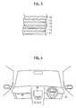
- the display apparatus is applicable as an automotive display apparatus such as a display apparatus 22 which a navigation or audio/visual system mounted on a vehicle includes, and as an in-meter display apparatus 21 mounted on a dashboard in front of a driver's seat of the vehicle.
- a light environment laboratory in which a light source with illuminance of more than 5000 lx is placed, is used as a test place, and an evaluator who wears the sunglasses having the polarization function sits down on a driver's seat of an actual vehicle.
- a menu screen of a car navigation system On a display screen attached onto a center console in the actual vehicle, a menu screen of a car navigation system is displayed.
- the display screen was attached at a position, which is downward by 30° from an eyes' position of the evaluator, at a plane angle of 35° with respect to a vehicle traveling direction, and at a sight distance of approximately 700 mm. Brightness and contrast of the display screen are set at defaults.
- a light source is placed in a direction, which is upward by 20° from the evaluator and left rearward by 60° in the vehicle. Note that it is assumed that the polarization direction of the displayed image outputted from the display apparatus and the polarization direction of the sunglasses are in a state of the crossed Nicols.
- a raw material As a raw material, one is used, which is obtained by performing dispersion treatment for a 1-wt% aqueous solution of CEOLUS RC-591 made by Asahi Kasei Chemicals Corporation, which is a colloidal grade of crystallite cellulose, by using a high-pressure homogenizer for 10 minutes. To 500 ml of this solution, there were added: 25 mL of acetic anhydride; 400 mL of acetic acid; 500 mL of toluene; and 2.5 mL of perchloric acid, and a reaction was caused for a resultant mixture at room temperature for 1 hour, whereby a front surface of the cellulose was converted into acetyl.
- CEOLUS RC-591 made by Asahi Kasei Chemicals Corporation, which is a colloidal grade of crystallite cellulose
- Water-containing fiber thus obtained was adjusted into a suspension in which a fiber content was 0.1 weight%, water thereof was removed by filtration, and the fiber was formed into a sheet shape. Moreover, the sheet-shaped fiber was hot-pressed at 55° for 72 hours with a pressure of 15 kPa, and water was removed therefrom, whereby dry fiber sheet with a thickness of 50 ⁇ m was formed.
- the dry fiber sheet obtained by the above-described method was soaked into a UV curing adhesive FINETAC CT6010 (made by DIC Corporation) under a reduced pressure, and was left standing still for 12 hours. Thereafter, by using a belt conveyer type UV irradiation apparatus (Fusin F300 and LC6B Bench Top Conveyor made by Fusion Systems Co., Ltd.), the fiber sheet impregnated with the resin was irradiated with ultraviolet rays, and was cured. A total irradiation energy amount at this time was 5 J/cm 2 . In such a way, the polarization solving adhesive was prepared.
- FINETAC CT6010 made by DIC Corporation
- the dry fiber sheet obtained by the above-described method was soaked into photoinitiator-containing acrylic resin (TCDDMA) under a reduced pressure, and was left standing still for 12 hours. Thereafter, by using a belt conveyer type UV irradiation apparatus (Fusin F300 and LC6B Bench Top Conveyor made by Fusion Systems Co., Ltd.), the fiber sheet impregnated with the resin was irradiated with ultraviolet rays, and was cured. A total irradiation energy amount at this time was 20 J/cm 2 . Thereafter, the fiber sheet was annealed (subjected to heat treatment) at 160°C for two hours in a vacuum, and the polarization solving base material was prepared.
- TCDDMA photoinitiator-containing acrylic resin
- FIG. 1A shows a cross-sectional configuration of the display apparatus according to Example 1.
- the liquid crystal panel 31 has a configuration shown in FIG. 3 , and above the output side of the liquid crystal panel 31, the touch panel 34 of the electrostatic capacitance type is arranged while interposing the gas layer AL therebetween.
- the AR films 32 and 33 are pasted, respectively. In such a way, the reflection of light on the interface between the liquid crystal panel 31 and the gas layer AL and on the interface between the touch panel 34 and the gas layer AL is suppressed.
- the linear polarization layer 35 is stacked.
- the base material layer 37 is stacked while interposing the adhesive layer 36 therebetween.
- the adhesive layer 36 is composed of the polarization solving adhesive containing the polarization solving fiber
- the base material layer 37 is made of the front surface base material that does not contain the polarization solving fiber.
- the AR film 38 is stacked on the base material layer 37.
- the linear polarization film for use in the linear polarization layer 35 is one imparted with absorption dichroism in such a manner that, after a base material film made of PVA (polyvinyl alcohol) is dyed with iodine or organic dye, the base material film is uniaxially stretched to approximately two to three times to thereby array molecules of the dye regularly.
- This linear polarization film exerts a function to reduce the light transmittance without changing a color tone thereof.
- As the linear polarization layer 35 AG150 made by Nitto Denko Corporation is used.
- the AR films 32, 33 and 38 three-layer AR films of MFAR-Roll made by MeCan Imaging Inc. are used.
- FIG. 1B shows a cross-sectional configuration of the display apparatus according to Example 2.
- the adhesive layer 39 is composed of the acrylic adhesive that does not contain the polarization solving fiber
- the base material layer 40 is made of the polarization solving base material that contains the polarization solving fiber.
- Other points are the same as those of FIG. 1A , and a description thereof is omitted.
- FIG. 1C shows a cross-sectional configuration of the display apparatus according to Example 3.
- the adhesive layer 36 is composed of the polarization solving adhesive containing the polarization solving fiber
- the base material layer 40 is composed of the polarization solving base material containing the polarization solving fiber. That is to say, both of the base material layer 40 and the adhesive layer 36 contain the polarization solving fiber.
- Other points are the same as those of FIG. 1A , and a description thereof is omitted.
- FIG. 1D shows a cross-sectional configuration of the display apparatus according to Example 4.
- Example 4 on the output side of the liquid crystal panel 31, the touch panel 34 of the electrostatic capacitance type is directly stacked while interposing the bonding agent 41 therebetween, and the gas layer AL is not interposed therebetween. Hence, the AR films 32 and 33 for preventing the reflection are not interposed, either.
- the bonding agent 41 a UV-curing acrylic bonding material (KCPF3001 made by Foresight) is used.
- the base material layer 37 that does not contain the polarization solving fiber is stacked while interposing therebetween the adhesive layer 36 that contains the polarization solving fiber.
- the linear polarization layer 35 is not interposed between the touch panel 34 and the adhesive layer 36.
- Other points are the same as those of FIG. 1A , and a description thereof is omitted.
- FIG. 1E shows a cross-sectional configuration of the display apparatus according to Example 5.
- the adhesive layer 39 is composed of the acrylic adhesive that does not contain the polarization solving fiber
- the base material layer 40 is composed of the polarization solving base material that contains the polarization solving fiber.
- Other points are the same as those of FIG. 1D , and a description thereof is omitted.
- FIG. 1F shows a cross-sectional configuration of the display apparatus according to Example 6.
- the adhesive layer 36 is composed of the polarization solving adhesive containing the polarization solving fiber
- the base material layer 40 is composed of the polarization solving base material containing the polarization solving fiber. That is to say, both of the base material layer 40 and the adhesive layer 36 contain the polarization solving fiber.
- Other points are the same as those of FIG. 1D , and a description thereof is omitted.
- FIG. 1G shows a cross-sectional configuration of the display apparatus according to Example 7.
- the display apparatus according to Example 7 further includes the two phase difference films 42 and 43 inserted so as to sandwich the front and back surfaces of the touch panel 34 of the electrostatic capacitance type. Other points are the same as those of FIG. 1A , and a description thereof is omitted.
- FIG. 1H shows a cross-sectional configuration of the display apparatus according to Example 8.
- the adhesive layer 39 is composed of the acrylic adhesive that does not contain the polarization solving fiber
- the base material layer 40 is made of the polarization solving base material that contains the polarization solving fiber.
- Other points are the same as those of FIG. 1G , and a description thereof is omitted.
- FIG. 1I shows a cross-sectional configuration of the display apparatus according to Example 9.
- the adhesive layer 36 is composed of the polarization solving adhesive containing the polarization solving fiber
- the base material layer 40 is made of the polarization solving base material containing the polarization solving fiber. That is to say, both of the base material layer 40 and the adhesive layer 36 contain the polarization solving fiber.
- Other points are the same as those of FIG. 1G , and a description thereof is omitted.
- FIG. 2A shows a cross-sectional configuration of the display apparatus according to Example 10.
- the touch panel 45 of the resistance film type is placed while interposing the gas layer AL therebetween.
- the AG film 44 is pasted.
- the linear polarization layer 35 is stacked.
- the base material layer 37 is stacked while interposing the adhesive layer 36 therebetween.
- the adhesive layer 36 is composed of the polarization solving adhesive that contains the polarization solving fiber
- the base material layer 37 is made of the front surface base material that does not contain the polarization solving fiber.
- the AG film 46 is stacked on the base material layer 37.
- FIG. 2B shows a cross-sectional configuration of the display apparatus according to Example 11.
- the adhesive layer 39 is composed of the acrylic adhesive that does not contain the polarization solving fiber
- the base material layer 40 is made of the polarization solving base material that contains the polarization solving fiber.
- Other points are the same as those of FIG. 2A , and a description thereof is omitted.
- FIG. 2C shows a cross-sectional configuration of the display apparatus according to Example 12.
- the adhesive layer 36 is composed of the polarization solving adhesive containing the polarization solving fiber
- the base material layer 40 is made of the polarization solving base material containing the polarization solving fiber. That is to say, both of the base material layer 40 and the adhesive layer 36 contain the polarization solving fiber.
- Other points are the same as those of FIG. 2A , and a description thereof is omitted.
- FIG. 2D shows a cross-sectional configuration of the display apparatus according to Example 13.
- the display apparatus according to Example 13 is different therefrom in further including the two phase difference films 42 and 43 inserted so as to sandwich the front and back surfaces of the touch panel 45; however, is common thereto in other points.
- the display apparatus according to Example 13 is different therefrom in using the touch panel 45 of the resistance film type in place of the touch panel 34 of the electrostatic capacitance type; however, is common thereto in other points.
- FIG. 2E shows a cross-sectional configuration of the display apparatus according to Example 14.
- the adhesive layer 39 is composed of the acrylic adhesive that does not contain the polarization solving fiber
- the base material layer 40 is made of the polarization solving base material that contains the polarization solving fiber.
- Other points are the same as those of FIG. 2D , and a description thereof is omitted.
- FIG. 2F shows a cross-sectional configuration of the display apparatus according to Example 15.
- the adhesive layer 36 is composed of the polarization solving adhesive containing the polarization solving fiber
- the base material layer 40 is composed of the polarization solving base material containing the polarization solving fiber. That is to say, both of the base material layer 40 and the adhesive layer 36 contain the polarization solving fiber.
- Other points are the same as those of FIG. 2D , and a description thereof is omitted.
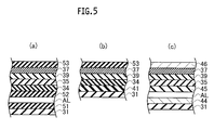
- FIG. 5A shows a cross-sectional configuration of the display apparatus according to Comparative example 1.
- the adhesive layer 39 is composed of the acrylic adhesive that does not contain the polarization solving fiber
- the base material layer 37 is made of the front surface base material that does not contain the polarization solving fiber. That is to say, the polarization solving fiber is not contained in either of the base material layer 40 and the adhesive layer 36.
- the display apparatus according to Comparative example 1 is different in using moss-eye films 51, 52 and 53 in place of the AR films 32, 33 and 38 having the multi-layer structure. Other points are the same as those of FIG. 1A , and a description thereof is omitted.
- FIG. 5B shows a cross-sectional configuration of the display apparatus according to Comparative example 2.
- the polarization solving fiber is not contained in either of the base material layer 40 and the adhesive layer 36 in a similar way to Comparative example 1.
- the display apparatus according to Comparative example 1 is different therefrom in using the moss-eye film 53 in place of the AR film 38 having the multi-layer structure. Other points are the same as those of FIG. 1D , and a description thereof is omitted.
- FIG. 5C shows a cross-sectional configuration of the display apparatus according to Comparative example 3. Also in Comparative example 3, the polarization solving fiber is not contained in either of the base material layer 40 and the adhesive layer 36 in a similar way to Comparative example 1. Other configurations are the same as those of FIG. 2A , and a description thereof is omitted.
- Table 1 shows the configurations and evaluation test results of the display apparatuses according to Examples 1 to 15 and Comparative examples 1 to 3, which are described above.
- a polarization solution degree in Table 1 represents a solution degree of the linear polarization of the displayed image outputted from the display apparatus. As shown in Table 1, it is understood that evaluations of the contrast, polarization solution degree and visibility of the displayed image are increased in the display apparatuses according to Examples 1 to 15, in each of which at least one of the adhesive layer and the base material layer contains the polarization solving fiber, in comparison with the display apparatuses according to Comparative examples 1 to 3, in each of which either of the adhesive layer and the base material layer does not contain the polarization solving fiber.
- At least one of the base material layers 36 and 39 and the adhesive layers 37 and 40 contains the polarization solving fiber, whereby the polarization solving fiber solves the linear polarization of the displayed image, and can thereby enhance the visibility of the displayed image.
- the polarization solving fiber is contained in at least one of the base material layers 36 and 39 and the adhesive layers 37 and 40, and accordingly, it becomes unnecessary to stack a new layer for solving the polarization, and manufacturing cost can be suppressed to be low. At the same time, it becomes possible to thin the whole of the layers, and the light transmittance can be enhanced by reducing the haze. Hence, image quality of the displayed image is improved.
- the polarization solving fiber is contained in at least one of the base material layers 36 and 39 and the adhesive layers 37 and 40, and accordingly, irregularities of the fiber do not appear on the outermost front surface of the display apparatus. Therefore, a white blur can be suppressed by reducing the haze. Hence, the image quality of the displayed image is improved.
- the polarization solving fiber is an aggregate of the cellulose nano-fiber, the cellulose nano-fiber contains a hydroxyl group, a part of the hydroxyl group is chemically modified, a width of the fiber is 10 nm or more to 50 nm or less, and an aspect ratio of the fiber is 1 or more to 200 or less.
- the base material layers 36 and 39 and the adhesive layers 37 and 40 are located more on the output side of the displayed image than the linear polarization plate which the liquid crystal panel 31 includes. In such a way, the linear polarization can be suppressed from being generated again on the light which has transmitted through the base material layers 36 and 39 and the adhesive layers 37 and 40.
- the blend ratio of the polarization solving fiber is 1 weight% or more to 95 weight% or less with respect to the base material having the polarization solving properties, whereby a range of loading, which is optimum for striking a balance between the polarization solving properties and the transparency, can be set.
- the thickness of the member that contains the polarization solving fiber is 10 ⁇ m or more to 50 ⁇ m or less, whereby the transmittance can be enhanced by preventing the lowering of the haze. Moreover, at the same time, the unevenness of thickness is reduced, and the displayed image can be sharpened.
- the linear polarization layer 35 and the phase difference film 43 are interposed between the touch panels 34 and 45 and the adhesive layers 37 and 40, whereby the displayed image is circularly polarized, and accordingly, the polarization solution degree and the contrast of the displayed image are enhanced, and at the same time, the linear polarization layer 35 can effectively cut off the component of the light incident from the outside.
- the polarization solving fiber is contained in at least one of the base material layers 36 and 39 and the adhesive layers 37 and 40, whereby the linear polarization by the linear polarization layer 35 can be solved effectively.
- the touch panel 45 is the touch panel of the resistance film type
- the light reflected in the air layer contained in the inside of the touch panel 45 is increased, and accordingly, it is necessary to enhance the degree of the linear polarization in the linear polarization layer 35.
- the polarization solving fiber is contained in at least one of the base material layers 36 and 39 and the adhesive layers 37 and 40, whereby the linear polarization by the linear polarization layer 35 can be solved effectively.
- the drive information is presented by the displayed image in which the linear polarization is solved, and even if the driver wears the sunglasses having the polarization function, the lowering of the transmission light quantity and visibility can be suppressed.
- the base material layers 37 and 40 are pasted onto the touch panels 34 and 45 while interposing the adhesive layers 36 and 39 therebetween, whereby each of the stacked bodies LB1 and LB2 is formed. Thereafter, each of the stacked bodies LB1 and LB2 is placed onto the display screen of the liquid crystal panel 31.
- the number of parts count is reduced since the structure is simple, and moreover, the film forming process is also simplified in the event of the manufacture, and accordingly, the display device can be manufactured at low cost.
- the automotive display apparatus and the method for manufacturing the display apparatus according to the present invention the polarization solving properties of the displayed image are enhanced, whereby the visibility of the displayed image can be enhanced.
Landscapes
- Physics & Mathematics (AREA)
- Nonlinear Science (AREA)
- General Physics & Mathematics (AREA)
- Engineering & Computer Science (AREA)
- Optics & Photonics (AREA)
- Mathematical Physics (AREA)
- Chemical & Material Sciences (AREA)
- Crystallography & Structural Chemistry (AREA)
- Theoretical Computer Science (AREA)
- General Engineering & Computer Science (AREA)
- Human Computer Interaction (AREA)
- Liquid Crystal (AREA)
- Polarising Elements (AREA)
- Devices For Indicating Variable Information By Combining Individual Elements (AREA)
Applications Claiming Priority (2)
| Application Number | Priority Date | Filing Date | Title |
|---|---|---|---|
| JP2012029267A JP5861485B2 (ja) | 2012-02-14 | 2012-02-14 | 表示装置、自動車用表示装置、及び表示装置の製造方法 |
| PCT/JP2013/052989 WO2013121991A1 (ja) | 2012-02-14 | 2013-02-08 | 表示装置、自動車用表示装置、及び表示装置の製造方法 |
Publications (3)
| Publication Number | Publication Date |
|---|---|
| EP2816396A1 true EP2816396A1 (de) | 2014-12-24 |
| EP2816396A4 EP2816396A4 (de) | 2015-03-11 |
| EP2816396B1 EP2816396B1 (de) | 2018-05-02 |
Family
ID=48984103
Family Applications (1)
| Application Number | Title | Priority Date | Filing Date |
|---|---|---|---|
| EP13748824.3A Active EP2816396B1 (de) | 2012-02-14 | 2013-02-08 | Anzeigevorrichtung, anzeigevorrichtung für kraftfahrzeug und verfahren zur herstellung einer anzeigevorrichtung |
Country Status (5)
| Country | Link |
|---|---|
| US (1) | US9213198B2 (de) |
| EP (1) | EP2816396B1 (de) |
| JP (1) | JP5861485B2 (de) |
| CN (1) | CN104094168B (de) |
| WO (1) | WO2013121991A1 (de) |
Families Citing this family (8)
| Publication number | Priority date | Publication date | Assignee | Title |
|---|---|---|---|---|
| DE102013012110A1 (de) | 2013-07-12 | 2015-01-15 | e.solutions GmbH | Berührungsempfindlicher Bildschirm insbesondere zur Verwendung in einem Kraftfahrzeug |
| KR102187743B1 (ko) * | 2013-11-28 | 2020-12-07 | 엘지전자 주식회사 | 표시 장치 |
| CN112526665B (zh) | 2015-03-13 | 2023-01-03 | 三菱化学株式会社 | 光学薄膜和其制造方法 |
| WO2017018036A1 (ja) * | 2015-07-28 | 2017-02-02 | アルプス電気株式会社 | 積層構造体、積層構造体の製造方法および画像表示装置 |
| US20170057356A1 (en) * | 2015-08-27 | 2017-03-02 | James Frederick Krier | Seamless instrument cluster |
| JP7372106B2 (ja) * | 2018-10-15 | 2023-10-31 | 花王株式会社 | 粘着剤組成物 |
| JP7187990B2 (ja) * | 2018-11-01 | 2022-12-13 | 大日本印刷株式会社 | 樹脂成形体の製造方法 |
| JP7412900B2 (ja) * | 2019-05-09 | 2024-01-15 | リンテック株式会社 | 粘着剤組成物、及び粘着シート |
Family Cites Families (8)
| Publication number | Priority date | Publication date | Assignee | Title |
|---|---|---|---|---|
| JP2006018800A (ja) * | 2004-06-01 | 2006-01-19 | Nitto Denko Corp | 高耐久タッチパネル |
| WO2007055269A1 (ja) * | 2005-11-10 | 2007-05-18 | Sharp Kabushiki Kaisha | 液晶表示装置 |
| JP4905178B2 (ja) * | 2007-02-27 | 2012-03-28 | コニカミノルタホールディングス株式会社 | 光学フィルムの製造方法、光学フィルム、及びそれを用いた偏光板、液晶ディスプレイ |
| JP2008310309A (ja) * | 2007-05-11 | 2008-12-25 | Hitachi Chem Co Ltd | 液晶表示装置 |
| JP2008310310A (ja) * | 2007-05-15 | 2008-12-25 | Hitachi Chem Co Ltd | 偏光解消材料及びそれを用いた偏光解消素子、並びに、液晶表示装置 |
| JP5131983B2 (ja) * | 2008-10-06 | 2013-01-30 | 日東電工株式会社 | 光学積層体および画像表示装置 |
| JP5386955B2 (ja) | 2008-10-28 | 2014-01-15 | 宇部興産株式会社 | ポリアミド多孔質略球状粒子および光学材料 |
| WO2011105133A1 (ja) * | 2010-02-24 | 2011-09-01 | コニカミノルタオプト株式会社 | 表面改質樹脂フィルム、その製造方法、それを用いた偏光板、及び液晶表示装置 |
-
2012
- 2012-02-14 JP JP2012029267A patent/JP5861485B2/ja active Active
-
2013
- 2013-02-08 US US14/378,245 patent/US9213198B2/en active Active
- 2013-02-08 EP EP13748824.3A patent/EP2816396B1/de active Active
- 2013-02-08 WO PCT/JP2013/052989 patent/WO2013121991A1/ja not_active Ceased
- 2013-02-08 CN CN201380008231.0A patent/CN104094168B/zh active Active
Also Published As
| Publication number | Publication date |
|---|---|
| CN104094168A (zh) | 2014-10-08 |
| JP5861485B2 (ja) | 2016-02-16 |
| WO2013121991A1 (ja) | 2013-08-22 |
| US9213198B2 (en) | 2015-12-15 |
| EP2816396B1 (de) | 2018-05-02 |
| US20150009429A1 (en) | 2015-01-08 |
| EP2816396A4 (de) | 2015-03-11 |
| CN104094168B (zh) | 2016-11-02 |
| JP2013167672A (ja) | 2013-08-29 |
Similar Documents
| Publication | Publication Date | Title |
|---|---|---|
| EP2816396B1 (de) | Anzeigevorrichtung, anzeigevorrichtung für kraftfahrzeug und verfahren zur herstellung einer anzeigevorrichtung | |
| KR101682718B1 (ko) | 편광판 및 그것을 이용한 적층 광학 부재 | |
| CN102540289B (zh) | 一种光学扩散膜的制备方法及一种背光模组、一种液晶显示装置 | |
| CN108885362A (zh) | 调光装置 | |
| JP5131983B2 (ja) | 光学積層体および画像表示装置 | |
| JP2020129126A (ja) | 調光部材、サンバイザ及び移動体 | |
| TW200923506A (en) | A set of polarizer, and a liquid crystal panel and a liquid crystal display apparatus used thereof | |
| TWI443364B (zh) | 線性偏光區隔膜、線性偏光區隔層積膜、背光系統和液晶顯示器 | |
| KR20090020641A (ko) | 점착제가 형성된 편광 필름, 광학 적층체 및 편광 필름의 세트 | |
| JPWO2018105365A1 (ja) | 導光板、面発光装置及び導光板の製造方法 | |
| CN101261397A (zh) | 偏光片及液晶显示装置 | |
| CN102135663B (zh) | 一种汽车hud前挡玻璃 | |
| CN202472012U (zh) | 一种光学扩散膜 | |
| US6697132B2 (en) | Optical member and liquid crystal display device | |
| CN210514868U (zh) | 一种显示装置 | |
| TW201738596A (zh) | 偏光板之套組及使用該套組之ips模式液晶顯示裝置 | |
| KR101078599B1 (ko) | 일체형 고휘도 편광시트, 그를 적용한 액정디스플레이 패널후면용 편광필름 및 그를 구비한 액정디스플레이 | |
| JP5550869B2 (ja) | 液晶表示装置 | |
| US10018752B2 (en) | Diffusion sheet, backlight module and liquid crystal display device | |
| CN1837866A (zh) | 增亮整合型偏光膜/光学膜结构及制造方法及显示单元 | |
| JP2013054271A (ja) | 表示装置、自動車用表示装置、及び表示装置の製造方法 | |
| KR102848585B1 (ko) | 편광판 및 이를 포함하는 광학 표시 장치 | |
| CN210835508U (zh) | 一种光学膜片结构及其液晶模组 | |
| TW200946984A (en) | Polarizing plate, manufacturing method thereof and display device using the same | |
| JP2023107977A (ja) | 調光装置 |
Legal Events
| Date | Code | Title | Description |
|---|---|---|---|
| PUAI | Public reference made under article 153(3) epc to a published international application that has entered the european phase |
Free format text: ORIGINAL CODE: 0009012 |
|
| 17P | Request for examination filed |
Effective date: 20140723 |
|
| AK | Designated contracting states |
Kind code of ref document: A1 Designated state(s): AL AT BE BG CH CY CZ DE DK EE ES FI FR GB GR HR HU IE IS IT LI LT LU LV MC MK MT NL NO PL PT RO RS SE SI SK SM TR |
|
| AX | Request for extension of the european patent |
Extension state: BA ME |
|
| A4 | Supplementary search report drawn up and despatched |
Effective date: 20150205 |
|
| RIC1 | Information provided on ipc code assigned before grant |
Ipc: G09F 9/00 20060101ALI20150130BHEP Ipc: G06F 3/041 20060101ALI20150130BHEP Ipc: B60R 11/02 20060101ALI20150130BHEP Ipc: G02F 1/1333 20060101ALI20150130BHEP Ipc: G02F 1/1335 20060101AFI20150130BHEP Ipc: G02F 1/13363 20060101ALI20150130BHEP Ipc: G02B 5/30 20060101ALI20150130BHEP |
|
| DAX | Request for extension of the european patent (deleted) | ||
| 17Q | First examination report despatched |
Effective date: 20150914 |
|
| GRAP | Despatch of communication of intention to grant a patent |
Free format text: ORIGINAL CODE: EPIDOSNIGR1 |
|
| STAA | Information on the status of an ep patent application or granted ep patent |
Free format text: STATUS: GRANT OF PATENT IS INTENDED |
|
| INTG | Intention to grant announced |
Effective date: 20180104 |
|
| GRAS | Grant fee paid |
Free format text: ORIGINAL CODE: EPIDOSNIGR3 |
|
| GRAA | (expected) grant |
Free format text: ORIGINAL CODE: 0009210 |
|
| STAA | Information on the status of an ep patent application or granted ep patent |
Free format text: STATUS: THE PATENT HAS BEEN GRANTED |
|
| AK | Designated contracting states |
Kind code of ref document: B1 Designated state(s): AL AT BE BG CH CY CZ DE DK EE ES FI FR GB GR HR HU IE IS IT LI LT LU LV MC MK MT NL NO PL PT RO RS SE SI SK SM TR |
|
| REG | Reference to a national code |
Ref country code: GB Ref legal event code: FG4D |
|
| REG | Reference to a national code |
Ref country code: CH Ref legal event code: EP Ref country code: AT Ref legal event code: REF Ref document number: 995871 Country of ref document: AT Kind code of ref document: T Effective date: 20180515 |
|
| REG | Reference to a national code |
Ref country code: IE Ref legal event code: FG4D |
|
| REG | Reference to a national code |
Ref country code: DE Ref legal event code: R096 Ref document number: 602013036898 Country of ref document: DE |
|
| REG | Reference to a national code |
Ref country code: NL Ref legal event code: MP Effective date: 20180502 |
|
| REG | Reference to a national code |
Ref country code: LT Ref legal event code: MG4D |
|
| PG25 | Lapsed in a contracting state [announced via postgrant information from national office to epo] |
Ref country code: LT Free format text: LAPSE BECAUSE OF FAILURE TO SUBMIT A TRANSLATION OF THE DESCRIPTION OR TO PAY THE FEE WITHIN THE PRESCRIBED TIME-LIMIT Effective date: 20180502 Ref country code: SE Free format text: LAPSE BECAUSE OF FAILURE TO SUBMIT A TRANSLATION OF THE DESCRIPTION OR TO PAY THE FEE WITHIN THE PRESCRIBED TIME-LIMIT Effective date: 20180502 Ref country code: NO Free format text: LAPSE BECAUSE OF FAILURE TO SUBMIT A TRANSLATION OF THE DESCRIPTION OR TO PAY THE FEE WITHIN THE PRESCRIBED TIME-LIMIT Effective date: 20180802 Ref country code: ES Free format text: LAPSE BECAUSE OF FAILURE TO SUBMIT A TRANSLATION OF THE DESCRIPTION OR TO PAY THE FEE WITHIN THE PRESCRIBED TIME-LIMIT Effective date: 20180502 Ref country code: FI Free format text: LAPSE BECAUSE OF FAILURE TO SUBMIT A TRANSLATION OF THE DESCRIPTION OR TO PAY THE FEE WITHIN THE PRESCRIBED TIME-LIMIT Effective date: 20180502 Ref country code: BG Free format text: LAPSE BECAUSE OF FAILURE TO SUBMIT A TRANSLATION OF THE DESCRIPTION OR TO PAY THE FEE WITHIN THE PRESCRIBED TIME-LIMIT Effective date: 20180802 |
|
| PG25 | Lapsed in a contracting state [announced via postgrant information from national office to epo] |
Ref country code: RS Free format text: LAPSE BECAUSE OF FAILURE TO SUBMIT A TRANSLATION OF THE DESCRIPTION OR TO PAY THE FEE WITHIN THE PRESCRIBED TIME-LIMIT Effective date: 20180502 Ref country code: GR Free format text: LAPSE BECAUSE OF FAILURE TO SUBMIT A TRANSLATION OF THE DESCRIPTION OR TO PAY THE FEE WITHIN THE PRESCRIBED TIME-LIMIT Effective date: 20180803 Ref country code: NL Free format text: LAPSE BECAUSE OF FAILURE TO SUBMIT A TRANSLATION OF THE DESCRIPTION OR TO PAY THE FEE WITHIN THE PRESCRIBED TIME-LIMIT Effective date: 20180502 Ref country code: LV Free format text: LAPSE BECAUSE OF FAILURE TO SUBMIT A TRANSLATION OF THE DESCRIPTION OR TO PAY THE FEE WITHIN THE PRESCRIBED TIME-LIMIT Effective date: 20180502 Ref country code: HR Free format text: LAPSE BECAUSE OF FAILURE TO SUBMIT A TRANSLATION OF THE DESCRIPTION OR TO PAY THE FEE WITHIN THE PRESCRIBED TIME-LIMIT Effective date: 20180502 |
|
| REG | Reference to a national code |
Ref country code: AT Ref legal event code: MK05 Ref document number: 995871 Country of ref document: AT Kind code of ref document: T Effective date: 20180502 |
|
| PG25 | Lapsed in a contracting state [announced via postgrant information from national office to epo] |
Ref country code: DK Free format text: LAPSE BECAUSE OF FAILURE TO SUBMIT A TRANSLATION OF THE DESCRIPTION OR TO PAY THE FEE WITHIN THE PRESCRIBED TIME-LIMIT Effective date: 20180502 Ref country code: AT Free format text: LAPSE BECAUSE OF FAILURE TO SUBMIT A TRANSLATION OF THE DESCRIPTION OR TO PAY THE FEE WITHIN THE PRESCRIBED TIME-LIMIT Effective date: 20180502 Ref country code: PL Free format text: LAPSE BECAUSE OF FAILURE TO SUBMIT A TRANSLATION OF THE DESCRIPTION OR TO PAY THE FEE WITHIN THE PRESCRIBED TIME-LIMIT Effective date: 20180502 Ref country code: SK Free format text: LAPSE BECAUSE OF FAILURE TO SUBMIT A TRANSLATION OF THE DESCRIPTION OR TO PAY THE FEE WITHIN THE PRESCRIBED TIME-LIMIT Effective date: 20180502 Ref country code: EE Free format text: LAPSE BECAUSE OF FAILURE TO SUBMIT A TRANSLATION OF THE DESCRIPTION OR TO PAY THE FEE WITHIN THE PRESCRIBED TIME-LIMIT Effective date: 20180502 Ref country code: CZ Free format text: LAPSE BECAUSE OF FAILURE TO SUBMIT A TRANSLATION OF THE DESCRIPTION OR TO PAY THE FEE WITHIN THE PRESCRIBED TIME-LIMIT Effective date: 20180502 Ref country code: RO Free format text: LAPSE BECAUSE OF FAILURE TO SUBMIT A TRANSLATION OF THE DESCRIPTION OR TO PAY THE FEE WITHIN THE PRESCRIBED TIME-LIMIT Effective date: 20180502 |
|
| REG | Reference to a national code |
Ref country code: DE Ref legal event code: R097 Ref document number: 602013036898 Country of ref document: DE |
|
| PG25 | Lapsed in a contracting state [announced via postgrant information from national office to epo] |
Ref country code: IT Free format text: LAPSE BECAUSE OF FAILURE TO SUBMIT A TRANSLATION OF THE DESCRIPTION OR TO PAY THE FEE WITHIN THE PRESCRIBED TIME-LIMIT Effective date: 20180502 Ref country code: SM Free format text: LAPSE BECAUSE OF FAILURE TO SUBMIT A TRANSLATION OF THE DESCRIPTION OR TO PAY THE FEE WITHIN THE PRESCRIBED TIME-LIMIT Effective date: 20180502 |
|
| PLBE | No opposition filed within time limit |
Free format text: ORIGINAL CODE: 0009261 |
|
| STAA | Information on the status of an ep patent application or granted ep patent |
Free format text: STATUS: NO OPPOSITION FILED WITHIN TIME LIMIT |
|
| 26N | No opposition filed |
Effective date: 20190205 |
|
| PG25 | Lapsed in a contracting state [announced via postgrant information from national office to epo] |
Ref country code: SI Free format text: LAPSE BECAUSE OF FAILURE TO SUBMIT A TRANSLATION OF THE DESCRIPTION OR TO PAY THE FEE WITHIN THE PRESCRIBED TIME-LIMIT Effective date: 20180502 |
|
| REG | Reference to a national code |
Ref country code: CH Ref legal event code: PL |
|
| PG25 | Lapsed in a contracting state [announced via postgrant information from national office to epo] |
Ref country code: LU Free format text: LAPSE BECAUSE OF NON-PAYMENT OF DUE FEES Effective date: 20190208 Ref country code: MC Free format text: LAPSE BECAUSE OF FAILURE TO SUBMIT A TRANSLATION OF THE DESCRIPTION OR TO PAY THE FEE WITHIN THE PRESCRIBED TIME-LIMIT Effective date: 20180502 |
|
| REG | Reference to a national code |
Ref country code: BE Ref legal event code: MM Effective date: 20190228 |
|
| REG | Reference to a national code |
Ref country code: IE Ref legal event code: MM4A |
|
| PG25 | Lapsed in a contracting state [announced via postgrant information from national office to epo] |
Ref country code: AL Free format text: LAPSE BECAUSE OF FAILURE TO SUBMIT A TRANSLATION OF THE DESCRIPTION OR TO PAY THE FEE WITHIN THE PRESCRIBED TIME-LIMIT Effective date: 20180502 |
|
| PG25 | Lapsed in a contracting state [announced via postgrant information from national office to epo] |
Ref country code: LI Free format text: LAPSE BECAUSE OF NON-PAYMENT OF DUE FEES Effective date: 20190228 Ref country code: CH Free format text: LAPSE BECAUSE OF NON-PAYMENT OF DUE FEES Effective date: 20190228 |
|
| PG25 | Lapsed in a contracting state [announced via postgrant information from national office to epo] |
Ref country code: IE Free format text: LAPSE BECAUSE OF NON-PAYMENT OF DUE FEES Effective date: 20190208 |
|
| PG25 | Lapsed in a contracting state [announced via postgrant information from national office to epo] |
Ref country code: BE Free format text: LAPSE BECAUSE OF NON-PAYMENT OF DUE FEES Effective date: 20190228 |
|
| PG25 | Lapsed in a contracting state [announced via postgrant information from national office to epo] |
Ref country code: TR Free format text: LAPSE BECAUSE OF FAILURE TO SUBMIT A TRANSLATION OF THE DESCRIPTION OR TO PAY THE FEE WITHIN THE PRESCRIBED TIME-LIMIT Effective date: 20180502 |
|
| PG25 | Lapsed in a contracting state [announced via postgrant information from national office to epo] |
Ref country code: MT Free format text: LAPSE BECAUSE OF NON-PAYMENT OF DUE FEES Effective date: 20190208 Ref country code: PT Free format text: LAPSE BECAUSE OF FAILURE TO SUBMIT A TRANSLATION OF THE DESCRIPTION OR TO PAY THE FEE WITHIN THE PRESCRIBED TIME-LIMIT Effective date: 20180903 |
|
| PG25 | Lapsed in a contracting state [announced via postgrant information from national office to epo] |
Ref country code: CY Free format text: LAPSE BECAUSE OF FAILURE TO SUBMIT A TRANSLATION OF THE DESCRIPTION OR TO PAY THE FEE WITHIN THE PRESCRIBED TIME-LIMIT Effective date: 20180502 |
|
| PG25 | Lapsed in a contracting state [announced via postgrant information from national office to epo] |
Ref country code: IS Free format text: LAPSE BECAUSE OF FAILURE TO SUBMIT A TRANSLATION OF THE DESCRIPTION OR TO PAY THE FEE WITHIN THE PRESCRIBED TIME-LIMIT Effective date: 20180902 |
|
| PG25 | Lapsed in a contracting state [announced via postgrant information from national office to epo] |
Ref country code: HU Free format text: LAPSE BECAUSE OF FAILURE TO SUBMIT A TRANSLATION OF THE DESCRIPTION OR TO PAY THE FEE WITHIN THE PRESCRIBED TIME-LIMIT; INVALID AB INITIO Effective date: 20130208 |
|
| PG25 | Lapsed in a contracting state [announced via postgrant information from national office to epo] |
Ref country code: MK Free format text: LAPSE BECAUSE OF FAILURE TO SUBMIT A TRANSLATION OF THE DESCRIPTION OR TO PAY THE FEE WITHIN THE PRESCRIBED TIME-LIMIT Effective date: 20180502 |
|
| REG | Reference to a national code |
Ref country code: DE Ref legal event code: R084 Ref document number: 602013036898 Country of ref document: DE |
|
| REG | Reference to a national code |
Ref country code: GB Ref legal event code: 746 Effective date: 20230925 |
|
| PGFP | Annual fee paid to national office [announced via postgrant information from national office to epo] |
Ref country code: GB Payment date: 20260121 Year of fee payment: 14 |
|
| PGFP | Annual fee paid to national office [announced via postgrant information from national office to epo] |
Ref country code: DE Payment date: 20260121 Year of fee payment: 14 |
|
| PGFP | Annual fee paid to national office [announced via postgrant information from national office to epo] |
Ref country code: FR Payment date: 20260121 Year of fee payment: 14 |