EP2816571A2 - Induktor und elektronische Vorrichtung damit - Google Patents
Induktor und elektronische Vorrichtung damit Download PDFInfo
- Publication number
- EP2816571A2 EP2816571A2 EP13197132.7A EP13197132A EP2816571A2 EP 2816571 A2 EP2816571 A2 EP 2816571A2 EP 13197132 A EP13197132 A EP 13197132A EP 2816571 A2 EP2816571 A2 EP 2816571A2
- Authority
- EP
- European Patent Office
- Prior art keywords
- central portion
- inductor
- magnetic flux
- coil
- extension
- Prior art date
- Legal status (The legal status is an assumption and is not a legal conclusion. Google has not performed a legal analysis and makes no representation as to the accuracy of the status listed.)
- Granted
Links
Images


Classifications
-
- H—ELECTRICITY
- H01—ELECTRIC ELEMENTS
- H01F—MAGNETS; INDUCTANCES; TRANSFORMERS; SELECTION OF MATERIALS FOR THEIR MAGNETIC PROPERTIES
- H01F27/00—Details of transformers or inductances, in general
- H01F27/28—Coils; Windings; Conductive connections
-
- H—ELECTRICITY
- H01—ELECTRIC ELEMENTS
- H01F—MAGNETS; INDUCTANCES; TRANSFORMERS; SELECTION OF MATERIALS FOR THEIR MAGNETIC PROPERTIES
- H01F38/00—Adaptations of transformers or inductances for specific applications or functions
- H01F38/08—High-leakage transformers or inductances
-
- H—ELECTRICITY
- H01—ELECTRIC ELEMENTS
- H01F—MAGNETS; INDUCTANCES; TRANSFORMERS; SELECTION OF MATERIALS FOR THEIR MAGNETIC PROPERTIES
- H01F27/00—Details of transformers or inductances, in general
- H01F27/06—Mounting, supporting or suspending transformers, reactors or choke coils not being of the signal type
-
- H—ELECTRICITY
- H01—ELECTRIC ELEMENTS
- H01F—MAGNETS; INDUCTANCES; TRANSFORMERS; SELECTION OF MATERIALS FOR THEIR MAGNETIC PROPERTIES
- H01F27/00—Details of transformers or inductances, in general
- H01F27/24—Magnetic cores
-
- H—ELECTRICITY
- H01—ELECTRIC ELEMENTS
- H01F—MAGNETS; INDUCTANCES; TRANSFORMERS; SELECTION OF MATERIALS FOR THEIR MAGNETIC PROPERTIES
- H01F3/00—Cores, Yokes, or armatures
- H01F3/10—Composite arrangements of magnetic circuits
- H01F3/12—Magnetic shunt paths
-
- H—ELECTRICITY
- H01—ELECTRIC ELEMENTS
- H01F—MAGNETS; INDUCTANCES; TRANSFORMERS; SELECTION OF MATERIALS FOR THEIR MAGNETIC PROPERTIES
- H01F27/00—Details of transformers or inductances, in general
- H01F27/06—Mounting, supporting or suspending transformers, reactors or choke coils not being of the signal type
- H01F2027/065—Mounting on printed circuit boards
Definitions
- Apparatuses consistent with the exemplary embodiments relate to an inductor and an electronic device including the same. More particularly, the exemplary embodiments relate to an improved inductor which reduces a height of an inductor core and secures current capacity, and an electronic device including the same.
- a display apparatus includes an image display using a liquid crystal display (LCD), a light emitting diode (LED) and an organic light emitting diode (OLED).
- LCD liquid crystal display
- LED light emitting diode
- OLED organic light emitting diode
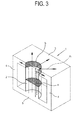
- FIGS. 1 to 3 illustrate a core of an inductor mounted on a PCB of an electronic device in the related art.
- the core 1 of the inductor is a hollow rectangular body including an upper portion 3, a lateral portion 4, a lower portion 5, and a cylindrical central portion 2, in which a coil is wounded around the central portion 2 to generate magnetic flux.
- the coil 6 is wound around the central portion 2 of the core 1.
- magnetic flux m is formed in the central portion 2 and passes through the central portion 2, the upper portion 3, the lateral portion 4, the lower portion 5 and then back to the central portion 2 as indicated by arrows.
- a bottleneck phenomenon occurs in an area f where magnetic flux vertically flowing in the central portion 2 curves to the upper portion 3.
- FIG. 3 is a cross-sectional view, taken along a center of the core 1, in which a cross section a of the central portion 2 and a cross section b of the upper portion 3 are shown as half of their actual sizes.
- the magnetic flux generated in the central portion 2 passes through the cross section a and then the cross section b of the upper portion 3.
- the cross section b has an area at least equivalent to or larger than the cross section a so that the bottleneck phenomenon of magnetic flux does not occur in the core 1.
- the upper portion 3 is formed thick so as to increase the area of the cross section b.
- the inductor In the thick inductor core, even a portion of the core where the bottleneck phenomenon does not occur is formed thick which causes an unnecessary waste of materials, raising production costs. Also, the inductor has a greater height, making it difficult to apply the inductor to an electronic device that is slim.
- An aspect of one or more exemplary embodiments is to reduce a height of an inductor core and to minimize a bottleneck phenomenon of magnetic flux which may occur in the inductor core.
- Another aspect of one or more exemplary embodiments is to provide an inductor which is installed in a slim electronic device, while securing current capacity.
- an inductor including: a coil in which an electric current flows; and a core that the coil is wound around, wherein the core includes a central portion that the coil is wound around; an extension which extends from opposite edges of the central portion according to a circulation path of magnetic flux generated by the electric current of the coil; and, lateral portions extending from the extension portions along the circulation path of the magnetic flux and facing the central portion with the coil disposed there between, and a first height at a first position of the extension portion on the circulation path of the magnetic flux which is spaced away from the edges of the central portion by a first distance which is larger than a second height at a second position on the circulation path of the magnetic spaced away from the edges of the central portion by a second distance which is longer than the first distance.
- a first cross section at the first position may have a predetermined area so that a bottleneck phenomenon of the magnetic flux is not generated at the first position.
- the area of the first cross section may be at least equivalent to or larger than a cross-sectional area of the central portion.
- a thickness of the extension portions at the first position may be larger than a thickness of the extension portions at the second position.
- the core may be provided such that a vertical side which the magnetic flux passes through along the circulation path of the magnetic flux has a uniform area.
- the extension portions may include a first extension portion formed above the central portion and a second extension portion formed under the central portion, where the second extension portion includes a connection terminal mounted on a printed circuit board and electrically connected thereto.
- At least one of the first extension portion and the second extension portion may include a protrusion which extends from one side thereof such that a thickness at the first position is larger than a thickness at the second position.
- an inductor including: a coil in which an electric current is configured to flow; and a core that the coil is wound around, wherein the core includes a central portion that the coil is wound around; an extension portion extending from opposite edges of the central according to a circulation path of magnetic flux generated by the electric current of the coil; and lateral portions extending from the extension portions along the circulation path of the magnetic flux and facing the central portion with the coil disposed there between, and the core is provided such that a vertical side which the magnetic flux passes through along the circulation path of the magnetic flux has a uniform area.
- the extension portions may include a first extension portion formed above the central portion and a second extension portion formed under the central portion, and the second extension portion includes a connection terminal mounted on a printed circuit board and electrically connected thereto.
- an electronic device including: a printed circuit board on which an electronic component to drive the electronic device is mounted; and an inductor mounted on the printed circuit board, wherein the inductor includes a coil in which an electric current is configured to flow and a core that the coil is wound around, the core includes a central portion that the coil is wound around, extension portions extending from opposite edges of the central portion according to a circulation path of magnetic flux generated by the electric current of the coil; and lateral portions extending from the extension along the circulation path of the magnetic flux and facing the central portion with the coil disposed there between, and a first height at a first position of the extension portions on the circulation path of the magnetic flux spaced away from the edges of the central portion by a first distance may be larger than a second height at a second position on the circulation path of the magnetic spaced away from the edges of the central portion by a second distance longer than the first distance.
- a first cross section at the first position may have a predetermined area so that a bottleneck phenomenon of the magnetic flux is not generated at the first position.
- the area of the first cross section is at least equivalent to or larger than a cross-sectional area of the central portion.
- a thickness of the extension portions at the first position may be larger than a thickness of the extension portions at the second position.
- the core may be provided such that a vertical side which the magnetic flux passes through along the circulation path of the magnetic flux has a uniform area.
- the extension portions may include a first extension portion formed above the central portion and a second extension portion formed under the central portion, and the second extension portion may include a connection terminal mounted on the printed circuit board and electrically connected thereto.
- At least one of the first extension portion and the second extension portion may include a protrusion extending from one side thereof such that a thickness at the first position is larger than a thickness at the second position.
- the printed circuit board may include a hole into which the protrusion is inserted.
- an electronic device including: a printed circuit board on which an electronic component to drive the electronic device is mounted; and an inductor mounted on the printed circuit board, wherein the inductor includes a coil in which an electric current is configured to flow and a core that the coil is wound around, the core includes a central portion that the coil is wound around, extension portions which extend from opposite edges of the central portion according to a circulation path of magnetic flux generated by the electric current of the coil; and lateral portions which extend from the extension portions along the circulation path of the magnetic flux and facing the central with the coil disposed there between, and the core is provided such that a vertical side which the magnetic flux passes through along the circulation path of the magnetic flux has a uniform area.
- the extension portions may include a first extension portion formed above the central portion and a second extension portion formed under the central portion, and the second extension portion includes a connection terminal mounted on the printed circuit board and electrically connected thereto.
- the first extension portion and the second extension portion may include a protrusion which extends from one side thereof.
- the printed circuit board may include a hole into which the protrusion is inserted.
- an inductor and an electronic device including the same may minimize a bottleneck phenomenon of magnetic flux which may occur in the inductor core, thereby securing the current capacity of the inductor.
- An aspect of an exemplary embodiment may provide an inductor including: a core including a central portion that a coil is configured to be wound around; extension portions which extend from opposite edges of the central portion; and lateral portions which extend from the extension portions along a circulation path of magnetic flux and facing the central portion, and a first height at a first position of the extension portions being spaced away from the edges of the central portion by a first distance which is larger than a second height at a second position which is spaced away from the edges of the central portion by a second distance which is longer than the first distance.
- the first height may be on a circulation path of the magnetic flux.
- the second height may further be on a circulation path of the magnetic flux.
- a first cross section at the first position has a predetermined area so that a bottleneck phenomenon of the magnetic flux is not generated at the first position.
- the area of the first cross section may be at least equivalent to or larger than a cross-sectional area of the central portion.
- a thickness of the extension portions at the first position may be larger than a thickness of the extension portions at the second position.
- the area of the first cross section may be at least equivalent to or larger than a cross-sectional area of the central portion.
- an inductor core includes an improved structure to resolve a bottleneck phenomenon of magnetic flux, with minimum use of core materials and to reduce a height of the inductor core, so that the inductor may be applied to various electronic devices.
- an inductor core has a minimized size while maintaining the current capacity of the inductor, thereby reducing production costs.
- an electronic device as set out in claim 11.
- FIGS. 4 to 6 illustrate an inductor core and an inductor mounted on a printed circuit board (PCB) of an electronic device according to an exemplary embodiment.
- PCB printed circuit board
- the inductor 10 includes a coil 80 in which an electric current flows and the core 20 which the coil 80 is wound around.
- the coil 80 is provided to obtain inductance of the inductor 10 and is formed of a wire having good conductivity.
- the coil 80 is formed by coating the wire with an insulating material and the coil 80 wound in a cylindrical or spiral shape for use.
- the core 20 includes a central portion 30 which the coil 80 is wound around, extension portions 40 and 60 extending from opposite edges of the central portion 30, and lateral portions 50 formed outside the central portions 30.
- the central portion 30 is provided in a cylindrical shape in a center of the inductor 10, and the coil 80 is wound around the central portion 30.
- an electric current flows in the coil 80 wound around the central portion 30, magnetic flux is generated.
- FIG. 5 when the electric current enters a right side of the coil and exits from a left side of the coil based on FIG. 5 , that is, when the electric current flows counterclockwise on the coil 80 wound around the central portion 30, viewed from a top of the core 20, the magnetic flux m is formed in the central portion 30 and travels in a vertically upward direction in the central portion 30 as indicated by arrows.
- the central portion 30 is designed to have a diameter and length which correspond to a desired inductance of the inductor 10.
- the central portion 30 is not limited to the aforementioned form but may have various shapes, for example, a rectangular pillar.
- the lateral portions 50 extend from the extension portions 40 and 60 and face the central portion 30 with the coil 80 disposed there between.
- the lateral portions 50 are provided to form a closed circulation path of the magnetic flux m which is formed in the central portion 30 to circulate back to the central portion 30.
- the portions 40 and 60 are formed in the shape of a rectangular plate which extends from the opposite edges of the central portion 30 and having a predetermined thickness t2.
- the extension portions 40 and 60 are not limited to the foregoing shape but may be formed in various shapes; for example, a circular shape.
- the extension portions 40 and 60 include a first extension portion 40 formed above the central portion 30 and a second extension portion 60 formed under the central portion 30.
- the extension portions 40 and 60 respectively include protrusions 42 and 62 which protrude with a larger diameter than the diameter of the central portion 30.
- the first extension portion 40 and the second extension portion 60 have the same shape, and thus the following description will be made with reference to the first extension portion 40.
- the magnetic flux m formed in the central portion 30 flows in the first extension portion 40.
- the magnetic flux m travelling vertically curves in a horizontal direction in an overlapping area of the central portion 30 and the first extension portion 40 and travels in the horizontal direction along the first extension portion 40 radially with respect to the central portion 30.
- a height t1 at a first position of the first extension portion 40 in contact with an edge of the central portion 30 is larger than a height t2 at a second position spaced away from the edge of the central portion 30 by a predetermined distance which is longer than the first position. That is, the protrusion 42 is formed with a height which becomes shorter from a center of the central portion 30 to the lateral portions 50.
- a height t1 of a first cross section b formed by vertically cutting from the edge of the central portion 30, that is, a boundary between the central portion 30 and the first extension portion 40, to an outside of the protrusion 42 is larger than a height t2 of a second cross section c having a predetermined radius r2 in an area of the first extension portion 40 where the protrusion 42 is not formed.
- the magnetic flux m travelling vertically (i.e. along the axis of the central portion) in the central portion 30 curves in the horizontal direction in the first cross section b. Magnetic flux through a surface is proportionate to a number of magnetic field lines passing through that surface.
- the magnetic flux m formed in the central portion 30 becomes concentrated in the first cross section b having the smaller area, causing a bottleneck phenomenon.
- the area of the first cross section b is at a predetermined level or higher.
- the area of the first cross section b may be at least equivalent to or larger than the cross-sectional area a of the central portion 30.
- FIG. 6 is a cross-sectional view formed by cutting across a center of the core 20.
- a cross section a of the central portion 30 and the first cross section b and the second cross section c of the first extension portion 40 are half of their actual sizes.
- FIG. 6 shows half of the cross sections, the following description will be made with reference to actual cross-sectional areas.
- the magnetic flux formed on the circular cross section travels radially from the central portion 30 in the first extension portion 40.
- the magnetic flux m formed on the cross section of the central portion 30 passes through an area in a circular band shape, such as the first cross section b and the second cross section c of the first extension portion 40.
- the central portion 30 has a radius of r1, the area of the cross section a is ⁇ r1 2 and the area of the first cross section b where the magnetic flux curves to the first extension portion 40 is 2 ⁇ r1t1.
- the area of the first cross section b is at least equivalent to or larger than the area of the cross section a of the central portion 30. That is, to satisfy ⁇ r1 2 ⁇ 2 ⁇ r1t1, the height t1 of the first cross section b is equivalent to or larger than half of the radius r1 of the central portion 30.
- the area of the second cross section c is 2 ⁇ r2t2.
- the bottleneck phenomenon of magnetic field does not occur without increasing the height thereof as in the first cross section b.
- the second extension portion 60 may be involved in the bottleneck phenomenon of magnetic flux on a boundary with the central portion 30, since the magnetic flux m passing through the lateral portions 50 curves back to the central portion 30.
- the protrusion 62 may be provided on the second extension portion 60 in the same manner as on the first extension portion 40.
- the second extension portion 60 includes a connection terminal 70 mounted on the PCB and electrically connectable thereto.
- the core 20 is not limited to the foregoing shape but may be formed for resolving the bottleneck phenomenon of magnetic flux such that a vertical side through which magnetic flux passes along the circulation path of the magnetic flux has a uniform area across the core 20.
- a pair of cores 20 may be provided in a form such that upper and lower portions formed by horizontally cutting across the center of the core 20 have the same form.
- FIG. 7 is a cross-sectional view which schematically illustrates an inductor core according to another exemplary embodiment.
- the core 100 may include a body 110 having an E-shaped cross section and a base 120 combined with a lower portion of the body 110.
- the body 110 includes a central portion 111 in a cylindrical shape that a coil is wound around, an upper portion 112 which extends from an upper portion of the central portion 111 and a lateral portion 113 which extends from an end of the upper portion 112 and disposed outside the central portion 111 to encompass the central portion 111.
- the upper portion 112 includes a protrusion 114 that protrudes outwards with a larger diameter than a diameter of the central portion 111 to prevent a bottleneck phenomenon of the magnetic field.
- the base 120 is formed in the same shape as the upper portion 112 and combined with a lower portion of the body 110.
- the base 120 includes a protrusion 124 which protrudes outwards in the same manner as the upper portion 112. This structure enables magnetic flux generated in the central portion 111 to form a closed circulation path, traveling through the upper portion 112, the lateral portion 113 and the base 120 and then back to the central portion 111.
- FIG. 8 is a cross-sectional view which schematically illustrates an inductor core with a different shape of a protrusion, according to an exemplary embodiment.
- the core 200 includes a central portion 220 that is provided in a cylindrical shape in a center of the inductor and that a coil is wound there around, extension portions 230 and 250 which extend from opposite edges of the central portion 220 and have a predetermined thickness, and lateral portions 240 which extend from the extension portions 230 and 250 and disposed outside the central portion 220.
- the extension portions 230 and 250 may respectively include protrusions 232 and 252 which protrude outwards to enable magnetic flux generated in the central portion 220 to smoothly travel without generation of the bottleneck phenomenon.
- the protrusions 232 and 252 are provided to increase an area of only a region where a bottleneck phenomenon of magnetic flux occurs and are formed in a ring shape having the same diameter as that of the central portion 220 and predetermined internal and external thicknesses. With this structure, a bottleneck phenomenon of magnetic flux may be resolved while minimizing materials of the core 200.
- a pair of cores 200 may be provided in a form such that upper and lower portions formed by horizontally cutting across the center of the core 200 have the same shape.
- the core 200 may have a base in the same manner as the core 100 of FIG. 7 .
- FIG. 9 is a block diagram which schematically illustrating a configuration of an electronic device 300 according to an exemplary embodiment.
- the electronic device 300 includes a communicator 310 configured to receive a data signal from the outside, a driver 350 configured to perform a preset operation which corresponds to the signal received through the communicator 310, a storage 340 configured to store information needed for the operation of the driver 350 and a program, a display 330 configured to display an image, and a power circuit 360 configured to be supplied with external power to supply power needed for driving the foregoing components.
- the inductor according to the exemplary embodiment may be mounted on a PCB of the power circuit 360 or the driver 350.
- the inductor may be formed with a minimized height, securing output capacity, thereby being applied to the electronic device 300 which is manufactured to be slim.
- FIG. 10 is a cross-sectional view which comprises a inductor i of the related art and the inductor 10 according to an exemplary embodiment which has the same capacity and is mounted on PCBs 90.
- the inductor 1 of the related art is formed with upper and lower portions having a sufficiently thick height to prevent a bottleneck phenomenon of magnetic flux.
- the inductor 10 includes protrusions 42 and 62 formed at upper and lower portions of the core only in an area where a bottleneck phenomenon occurs so as to prevent a bottleneck phenomenon of magnetic flux.
- a hole 92 into which the lower protrusion 62 is inserted is provided on the PCB 90.
- the inductor 10 is mounted on the PCB 90, the lower protrusion 62 is inserted into the hole 92 and an area where the protrusion 62 is not formed rests on PCB 90.
- a mounted height of the inductor 10 may be reduced by h as compared with a mounted height of the inductor 1 in the related art.
- Embodiments of the present invention provide an inductor comprising: a coil in which an electric current is configured to flow; and a core that the coil is wound around; wherein the core comprises a central portion that the coil is wound around; extension portions which extend from opposite edges of the central portion according to a circulation path of magnetic flux generated by the electric current of the coil; and lateral portions which extend from the extension portions along the circulation path of the magnetic flux and facing the central portion with the coil disposed there between; and wherein a first height at a first position of the extension portions on the circulation path of the magnetic flux spaced away from the edges of the central portion by a first distance which is larger than a second height at a second position on the circulation path of the magnetic spaced away from the edges of the central portion by a second distance which is longer than the first distance.
- the thickness of the extension portions at the first position is larger than a thickness of the extension portions at the second position.
- the first height comprises a protrusion that extends in a ring shape around the central portion.
- the first height comprises a protrusion that overlaps the edge of the central portion (e.g. a dome shaped protrusion, the base of which is larger than the cross section of the central portion).
- the extension portions comprise a first extension portion formed on one side of the central portion (e.g. above) and a second extension portion formed on an opposite side of the central portion (e.g. below).
- the second extension portion may comprise a connection terminal mounted on a printed circuit board and electrically connected thereto.
- At least one of the first extension portion and the second extension portion comprises a protrusion extending from one side thereof such that a thickness at the first position is larger than a thickness at the second position.
- the protrusions may have a larger diameter than the diameter of the central portion.
- the protrusions may be shaped to overlap a boundary region of the extension portions and the central portion. For example, if the central portion was cylindrical, such protrusions may be ring shaped.
- Embodiments of the present invention also provide an electronic device comprising such an inductor.
Landscapes
- Engineering & Computer Science (AREA)
- Power Engineering (AREA)
- Chemical & Material Sciences (AREA)
- Composite Materials (AREA)
- Coils Or Transformers For Communication (AREA)
Applications Claiming Priority (1)
| Application Number | Priority Date | Filing Date | Title |
|---|---|---|---|
| KR1020130069060A KR102070051B1 (ko) | 2013-06-17 | 2013-06-17 | 인덕터 및 이를 포함하는 전자장치 |
Publications (3)
| Publication Number | Publication Date |
|---|---|
| EP2816571A2 true EP2816571A2 (de) | 2014-12-24 |
| EP2816571A3 EP2816571A3 (de) | 2017-05-10 |
| EP2816571B1 EP2816571B1 (de) | 2020-09-16 |
Family
ID=49753095
Family Applications (1)
| Application Number | Title | Priority Date | Filing Date |
|---|---|---|---|
| EP13197132.7A Active EP2816571B1 (de) | 2013-06-17 | 2013-12-13 | Induktor und elektronische Vorrichtung damit |
Country Status (4)
| Country | Link |
|---|---|
| US (1) | US10229783B2 (de) |
| EP (1) | EP2816571B1 (de) |
| KR (1) | KR102070051B1 (de) |
| CN (1) | CN104240897B (de) |
Families Citing this family (2)
| Publication number | Priority date | Publication date | Assignee | Title |
|---|---|---|---|---|
| EP3456080A1 (de) | 2016-05-10 | 2019-03-20 | Netsia, Inc. | System und verfahren zur kommunikation zwischen programmierbaren basisstationen und softwaredefinierten funkzugangsnetzwerksteuergeräten |
| KR102520719B1 (ko) * | 2018-08-14 | 2023-04-12 | 삼성전자주식회사 | 인덕터 |
Family Cites Families (37)
| Publication number | Priority date | Publication date | Assignee | Title |
|---|---|---|---|---|
| US416762A (en) * | 1889-12-10 | Induction-coil | ||
| CA553564A (en) | 1958-02-25 | B. Williams Stanley | Transformer with five-leg core | |
| US2030648A (en) * | 1931-06-25 | 1936-02-11 | Gen Electric | Magnet system |
| US2513160A (en) * | 1945-10-02 | 1950-06-27 | Rca Corp | Transformer |
| US2779926A (en) * | 1954-01-25 | 1957-01-29 | Gen Electric | Transformer with five-leg core |
| GB968517A (en) * | 1961-12-05 | 1964-09-02 | Ferranti Ltd | Improvements relating to transductors |
| US3755767A (en) * | 1972-12-15 | 1973-08-28 | Gen Motors Corp | Variable inductance device |
| US4047138A (en) * | 1976-05-19 | 1977-09-06 | General Electric Company | Power inductor and transformer with low acoustic noise air gap |
| JPS5443533A (en) * | 1977-09-13 | 1979-04-06 | Matsushita Electric Ind Co Ltd | Manufacturing method of leakage-type transformer core |
| DE3503348C1 (de) * | 1985-02-01 | 1986-06-19 | Dr.Ing.H.C. F. Porsche Ag, 7000 Stuttgart | Ferromagnetischer Mehrfachschalenkern fuer elektrische Spulen |
| US5168440A (en) * | 1991-10-02 | 1992-12-01 | International Business Machines Corporation | Transformer/rectifier assembly with a figure eight secondary structure |
| US5382937A (en) * | 1992-07-30 | 1995-01-17 | Tdk Corporation | Coil device |
| JPH07297055A (ja) | 1994-04-26 | 1995-11-10 | Matsushita Electric Ind Co Ltd | チョークコイル |
| GB2296387B (en) * | 1994-12-02 | 1999-10-13 | Dale Electronics | Low profile inductor/transformer component |
| US5684446A (en) * | 1996-10-21 | 1997-11-04 | Abb Power T&D Company Inc. | Transformer core-coil frame attachment and ground |
| FR2769787B1 (fr) * | 1997-10-09 | 1999-12-24 | Ge Medical Syst Sa | Support modulaire pour les elements fonctionnels d'un bloc d'alimentation haute-tension et bloc ainsi obtenu |
| US6380834B1 (en) * | 2000-03-01 | 2002-04-30 | Space Systems/Loral, Inc. | Planar magnetic assembly |
| JP2002083724A (ja) * | 2000-09-08 | 2002-03-22 | Tokin Corp | 磁芯及び磁気素子 |
| TW467382U (en) * | 2000-12-20 | 2001-12-01 | Delta Electronics Inc | Embedded transformer |
| US6727793B2 (en) * | 2001-08-21 | 2004-04-27 | Astec International Limited | Low-power transformer for printed circuit boards |
| KR100464095B1 (ko) * | 2002-08-09 | 2005-01-03 | 삼성전자주식회사 | 트랜스포머의 보빈 고정장치 |
| US7046111B2 (en) | 2002-11-18 | 2006-05-16 | Illinoise Tool Works Inc. | Inductor assembly |
| US6844802B2 (en) * | 2003-06-18 | 2005-01-18 | Advanced Energy Industries, Inc. | Parallel core electromagnetic device |
| US7598837B2 (en) * | 2003-07-08 | 2009-10-06 | Pulse Engineering, Inc. | Form-less electronic device and methods of manufacturing |
| JP4576911B2 (ja) * | 2004-07-15 | 2010-11-10 | パナソニック株式会社 | コイル部品 |
| TWI272623B (en) | 2005-12-29 | 2007-02-01 | Ind Tech Res Inst | Power inductor with heat dissipating structure |
| TWI446378B (zh) * | 2007-03-23 | 2014-07-21 | Delta Electronics Inc | 表面黏著型磁性元件 |
| WO2008152616A1 (en) * | 2007-06-11 | 2008-12-18 | Moog Limited | Low-profile transformer |
| US8142870B2 (en) * | 2007-12-13 | 2012-03-27 | Personics Holdings Inc. | Energy responsive conformal device |
| US7564335B1 (en) * | 2008-04-07 | 2009-07-21 | Kevin Yang | Transformer hook mount |
| JP4760874B2 (ja) * | 2008-08-12 | 2011-08-31 | Tdk株式会社 | コイル巻線、及びコイル部品 |
| JP4737464B2 (ja) * | 2008-12-24 | 2011-08-03 | Tdk株式会社 | 縦型コイル部品 |
| US8242870B1 (en) * | 2009-04-13 | 2012-08-14 | Universal Lighting Technologies, Inc. | Magnetic component with a notched magnetic core structure |
| TWI389149B (zh) * | 2010-08-26 | 2013-03-11 | Acbel Polytech Inc | Symmetrical leakage inductance adjustable flat transformer |
| CN102592803B (zh) | 2011-01-05 | 2015-02-18 | 台达电子工业股份有限公司 | 可调整高度的变压器 |
| CN203027520U (zh) * | 2011-12-09 | 2013-06-26 | 特电株式会社 | 环状金属件感应加热装置和杯状金属件感应加热装置 |
| US9251945B2 (en) * | 2013-04-09 | 2016-02-02 | Fred O. Barthold | Planar core with high magnetic volume utilization |
-
2013
- 2013-06-17 KR KR1020130069060A patent/KR102070051B1/ko not_active Expired - Fee Related
- 2013-12-13 EP EP13197132.7A patent/EP2816571B1/de active Active
-
2014
- 2014-04-04 US US14/245,258 patent/US10229783B2/en active Active
- 2014-06-06 CN CN201410250661.XA patent/CN104240897B/zh active Active
Also Published As
| Publication number | Publication date |
|---|---|
| US20140368306A1 (en) | 2014-12-18 |
| CN104240897A (zh) | 2014-12-24 |
| EP2816571B1 (de) | 2020-09-16 |
| KR102070051B1 (ko) | 2020-01-29 |
| KR20140146405A (ko) | 2014-12-26 |
| US10229783B2 (en) | 2019-03-12 |
| CN104240897B (zh) | 2019-11-01 |
| EP2816571A3 (de) | 2017-05-10 |
Similar Documents
| Publication | Publication Date | Title |
|---|---|---|
| US8648685B2 (en) | Transformer and flat panel display device including the same | |
| US8698586B2 (en) | Transformer and flat panel display device including the same | |
| US8866576B2 (en) | Transformer and display device using the same | |
| US8643459B2 (en) | Transformer and flat panel display device including the same | |
| US20160141088A1 (en) | Magnetic component | |
| JP2014179585A (ja) | 電子自動車用変圧器モジュール | |
| KR20200082040A (ko) | 다중 코일을 이용한 무선 충전 장치 | |
| US10229783B2 (en) | Inductor and electronic device including the same | |
| JP5247788B2 (ja) | スリム型高電圧トランスフォーマー(slimtypehighvoltagetransformer) | |
| KR101039276B1 (ko) | 슬림형 고전압 트랜스포머 | |
| US8378770B2 (en) | Inductor assembly | |
| CN102074341B (zh) | 变压器结构 | |
| JP5949841B2 (ja) | トランスフォーマ及びこれを備えるフラットパネルディスプレイ装置 | |
| US20120169445A1 (en) | Transformer and flat panel display device having the same | |
| KR20140141986A (ko) | 인덕터 및 이를 포함하는 디스플레이장치 | |
| US20150302977A1 (en) | Coil structure and electric power conversion device | |
| JP7198128B2 (ja) | コイル部品、電子装置 | |
| CN105656218A (zh) | 感量可调节的无线供电发射、接收线圈 | |
| US20130194767A1 (en) | Multi-inductor usable with slim flat image display apparatus | |
| KR20180077599A (ko) | 무선 전력 송신 장치 | |
| KR102879511B1 (ko) | 인덕터 | |
| US20140354393A1 (en) | Electronic appartus | |
| KR101171640B1 (ko) | 트랜스포머 및 이를 구비하는 평판 디스플레이 장치 | |
| JP2023047604A (ja) | コイル部品 | |
| CN103366934B (zh) | 变压器结构 |
Legal Events
| Date | Code | Title | Description |
|---|---|---|---|
| PUAI | Public reference made under article 153(3) epc to a published international application that has entered the european phase |
Free format text: ORIGINAL CODE: 0009012 |
|
| 17P | Request for examination filed |
Effective date: 20131213 |
|
| AK | Designated contracting states |
Kind code of ref document: A2 Designated state(s): AL AT BE BG CH CY CZ DE DK EE ES FI FR GB GR HR HU IE IS IT LI LT LU LV MC MK MT NL NO PL PT RO RS SE SI SK SM TR |
|
| AX | Request for extension of the european patent |
Extension state: BA ME |
|
| PUAL | Search report despatched |
Free format text: ORIGINAL CODE: 0009013 |
|
| AK | Designated contracting states |
Kind code of ref document: A3 Designated state(s): AL AT BE BG CH CY CZ DE DK EE ES FI FR GB GR HR HU IE IS IT LI LT LU LV MC MK MT NL NO PL PT RO RS SE SI SK SM TR |
|
| AX | Request for extension of the european patent |
Extension state: BA ME |
|
| RIC1 | Information provided on ipc code assigned before grant |
Ipc: H01F 27/06 20060101ALI20170401BHEP Ipc: H01F 3/12 20060101AFI20170401BHEP Ipc: H01F 38/08 20060101ALN20170401BHEP |
|
| STAA | Information on the status of an ep patent application or granted ep patent |
Free format text: STATUS: REQUEST FOR EXAMINATION WAS MADE |
|
| R17P | Request for examination filed (corrected) |
Effective date: 20170718 |
|
| RBV | Designated contracting states (corrected) |
Designated state(s): AL AT BE BG CH CY CZ DE DK EE ES FI FR GB GR HR HU IE IS IT LI LT LU LV MC MK MT NL NO PL PT RO RS SE SI SK SM TR |
|
| STAA | Information on the status of an ep patent application or granted ep patent |
Free format text: STATUS: EXAMINATION IS IN PROGRESS |
|
| 17Q | First examination report despatched |
Effective date: 20190612 |
|
| GRAP | Despatch of communication of intention to grant a patent |
Free format text: ORIGINAL CODE: EPIDOSNIGR1 |
|
| STAA | Information on the status of an ep patent application or granted ep patent |
Free format text: STATUS: GRANT OF PATENT IS INTENDED |
|
| RIC1 | Information provided on ipc code assigned before grant |
Ipc: H01F 38/08 20060101ALN20200305BHEP Ipc: H01F 3/12 20060101AFI20200305BHEP Ipc: H01F 27/06 20060101ALI20200305BHEP |
|
| INTG | Intention to grant announced |
Effective date: 20200406 |
|
| GRAS | Grant fee paid |
Free format text: ORIGINAL CODE: EPIDOSNIGR3 |
|
| GRAA | (expected) grant |
Free format text: ORIGINAL CODE: 0009210 |
|
| STAA | Information on the status of an ep patent application or granted ep patent |
Free format text: STATUS: THE PATENT HAS BEEN GRANTED |
|
| AK | Designated contracting states |
Kind code of ref document: B1 Designated state(s): AL AT BE BG CH CY CZ DE DK EE ES FI FR GB GR HR HU IE IS IT LI LT LU LV MC MK MT NL NO PL PT RO RS SE SI SK SM TR |
|
| RAP1 | Party data changed (applicant data changed or rights of an application transferred) |
Owner name: SAMSUNG ELECTRONICS CO., LTD. |
|
| REG | Reference to a national code |
Ref country code: GB Ref legal event code: FG4D |
|
| REG | Reference to a national code |
Ref country code: CH Ref legal event code: EP |
|
| REG | Reference to a national code |
Ref country code: DE Ref legal event code: R096 Ref document number: 602013072553 Country of ref document: DE |
|
| REG | Reference to a national code |
Ref country code: IE Ref legal event code: FG4D |
|
| REG | Reference to a national code |
Ref country code: AT Ref legal event code: REF Ref document number: 1314890 Country of ref document: AT Kind code of ref document: T Effective date: 20201015 |
|
| PG25 | Lapsed in a contracting state [announced via postgrant information from national office to epo] |
Ref country code: FI Free format text: LAPSE BECAUSE OF FAILURE TO SUBMIT A TRANSLATION OF THE DESCRIPTION OR TO PAY THE FEE WITHIN THE PRESCRIBED TIME-LIMIT Effective date: 20200916 Ref country code: SE Free format text: LAPSE BECAUSE OF FAILURE TO SUBMIT A TRANSLATION OF THE DESCRIPTION OR TO PAY THE FEE WITHIN THE PRESCRIBED TIME-LIMIT Effective date: 20200916 Ref country code: NO Free format text: LAPSE BECAUSE OF FAILURE TO SUBMIT A TRANSLATION OF THE DESCRIPTION OR TO PAY THE FEE WITHIN THE PRESCRIBED TIME-LIMIT Effective date: 20201216 Ref country code: GR Free format text: LAPSE BECAUSE OF FAILURE TO SUBMIT A TRANSLATION OF THE DESCRIPTION OR TO PAY THE FEE WITHIN THE PRESCRIBED TIME-LIMIT Effective date: 20201217 Ref country code: BG Free format text: LAPSE BECAUSE OF FAILURE TO SUBMIT A TRANSLATION OF THE DESCRIPTION OR TO PAY THE FEE WITHIN THE PRESCRIBED TIME-LIMIT Effective date: 20201216 Ref country code: HR Free format text: LAPSE BECAUSE OF FAILURE TO SUBMIT A TRANSLATION OF THE DESCRIPTION OR TO PAY THE FEE WITHIN THE PRESCRIBED TIME-LIMIT Effective date: 20200916 |
|
| REG | Reference to a national code |
Ref country code: AT Ref legal event code: MK05 Ref document number: 1314890 Country of ref document: AT Kind code of ref document: T Effective date: 20200916 |
|
| REG | Reference to a national code |
Ref country code: NL Ref legal event code: MP Effective date: 20200916 |
|
| PG25 | Lapsed in a contracting state [announced via postgrant information from national office to epo] |
Ref country code: LV Free format text: LAPSE BECAUSE OF FAILURE TO SUBMIT A TRANSLATION OF THE DESCRIPTION OR TO PAY THE FEE WITHIN THE PRESCRIBED TIME-LIMIT Effective date: 20200916 Ref country code: RS Free format text: LAPSE BECAUSE OF FAILURE TO SUBMIT A TRANSLATION OF THE DESCRIPTION OR TO PAY THE FEE WITHIN THE PRESCRIBED TIME-LIMIT Effective date: 20200916 |
|
| REG | Reference to a national code |
Ref country code: LT Ref legal event code: MG4D |
|
| PG25 | Lapsed in a contracting state [announced via postgrant information from national office to epo] |
Ref country code: RO Free format text: LAPSE BECAUSE OF FAILURE TO SUBMIT A TRANSLATION OF THE DESCRIPTION OR TO PAY THE FEE WITHIN THE PRESCRIBED TIME-LIMIT Effective date: 20200916 Ref country code: SM Free format text: LAPSE BECAUSE OF FAILURE TO SUBMIT A TRANSLATION OF THE DESCRIPTION OR TO PAY THE FEE WITHIN THE PRESCRIBED TIME-LIMIT Effective date: 20200916 Ref country code: PT Free format text: LAPSE BECAUSE OF FAILURE TO SUBMIT A TRANSLATION OF THE DESCRIPTION OR TO PAY THE FEE WITHIN THE PRESCRIBED TIME-LIMIT Effective date: 20210118 Ref country code: NL Free format text: LAPSE BECAUSE OF FAILURE TO SUBMIT A TRANSLATION OF THE DESCRIPTION OR TO PAY THE FEE WITHIN THE PRESCRIBED TIME-LIMIT Effective date: 20200916 Ref country code: LT Free format text: LAPSE BECAUSE OF FAILURE TO SUBMIT A TRANSLATION OF THE DESCRIPTION OR TO PAY THE FEE WITHIN THE PRESCRIBED TIME-LIMIT Effective date: 20200916 Ref country code: EE Free format text: LAPSE BECAUSE OF FAILURE TO SUBMIT A TRANSLATION OF THE DESCRIPTION OR TO PAY THE FEE WITHIN THE PRESCRIBED TIME-LIMIT Effective date: 20200916 Ref country code: CZ Free format text: LAPSE BECAUSE OF FAILURE TO SUBMIT A TRANSLATION OF THE DESCRIPTION OR TO PAY THE FEE WITHIN THE PRESCRIBED TIME-LIMIT Effective date: 20200916 |
|
| PG25 | Lapsed in a contracting state [announced via postgrant information from national office to epo] |
Ref country code: ES Free format text: LAPSE BECAUSE OF FAILURE TO SUBMIT A TRANSLATION OF THE DESCRIPTION OR TO PAY THE FEE WITHIN THE PRESCRIBED TIME-LIMIT Effective date: 20200916 Ref country code: AL Free format text: LAPSE BECAUSE OF FAILURE TO SUBMIT A TRANSLATION OF THE DESCRIPTION OR TO PAY THE FEE WITHIN THE PRESCRIBED TIME-LIMIT Effective date: 20200916 Ref country code: AT Free format text: LAPSE BECAUSE OF FAILURE TO SUBMIT A TRANSLATION OF THE DESCRIPTION OR TO PAY THE FEE WITHIN THE PRESCRIBED TIME-LIMIT Effective date: 20200916 Ref country code: PL Free format text: LAPSE BECAUSE OF FAILURE TO SUBMIT A TRANSLATION OF THE DESCRIPTION OR TO PAY THE FEE WITHIN THE PRESCRIBED TIME-LIMIT Effective date: 20200916 Ref country code: IS Free format text: LAPSE BECAUSE OF FAILURE TO SUBMIT A TRANSLATION OF THE DESCRIPTION OR TO PAY THE FEE WITHIN THE PRESCRIBED TIME-LIMIT Effective date: 20210116 |
|
| REG | Reference to a national code |
Ref country code: DE Ref legal event code: R097 Ref document number: 602013072553 Country of ref document: DE |
|
| PG25 | Lapsed in a contracting state [announced via postgrant information from national office to epo] |
Ref country code: SK Free format text: LAPSE BECAUSE OF FAILURE TO SUBMIT A TRANSLATION OF THE DESCRIPTION OR TO PAY THE FEE WITHIN THE PRESCRIBED TIME-LIMIT Effective date: 20200916 |
|
| PLBE | No opposition filed within time limit |
Free format text: ORIGINAL CODE: 0009261 |
|
| STAA | Information on the status of an ep patent application or granted ep patent |
Free format text: STATUS: NO OPPOSITION FILED WITHIN TIME LIMIT |
|
| REG | Reference to a national code |
Ref country code: CH Ref legal event code: PL |
|
| 26N | No opposition filed |
Effective date: 20210617 |
|
| GBPC | Gb: european patent ceased through non-payment of renewal fee |
Effective date: 20201216 |
|
| PG25 | Lapsed in a contracting state [announced via postgrant information from national office to epo] |
Ref country code: DK Free format text: LAPSE BECAUSE OF FAILURE TO SUBMIT A TRANSLATION OF THE DESCRIPTION OR TO PAY THE FEE WITHIN THE PRESCRIBED TIME-LIMIT Effective date: 20200916 Ref country code: MC Free format text: LAPSE BECAUSE OF FAILURE TO SUBMIT A TRANSLATION OF THE DESCRIPTION OR TO PAY THE FEE WITHIN THE PRESCRIBED TIME-LIMIT Effective date: 20200916 Ref country code: SI Free format text: LAPSE BECAUSE OF FAILURE TO SUBMIT A TRANSLATION OF THE DESCRIPTION OR TO PAY THE FEE WITHIN THE PRESCRIBED TIME-LIMIT Effective date: 20200916 |
|
| REG | Reference to a national code |
Ref country code: BE Ref legal event code: MM Effective date: 20201231 |
|
| PG25 | Lapsed in a contracting state [announced via postgrant information from national office to epo] |
Ref country code: FR Free format text: LAPSE BECAUSE OF NON-PAYMENT OF DUE FEES Effective date: 20201231 Ref country code: LU Free format text: LAPSE BECAUSE OF NON-PAYMENT OF DUE FEES Effective date: 20201213 Ref country code: IE Free format text: LAPSE BECAUSE OF NON-PAYMENT OF DUE FEES Effective date: 20201213 Ref country code: IT Free format text: LAPSE BECAUSE OF FAILURE TO SUBMIT A TRANSLATION OF THE DESCRIPTION OR TO PAY THE FEE WITHIN THE PRESCRIBED TIME-LIMIT Effective date: 20200916 |
|
| PG25 | Lapsed in a contracting state [announced via postgrant information from national office to epo] |
Ref country code: LI Free format text: LAPSE BECAUSE OF NON-PAYMENT OF DUE FEES Effective date: 20201231 Ref country code: GB Free format text: LAPSE BECAUSE OF NON-PAYMENT OF DUE FEES Effective date: 20201216 Ref country code: CH Free format text: LAPSE BECAUSE OF NON-PAYMENT OF DUE FEES Effective date: 20201231 |
|
| PG25 | Lapsed in a contracting state [announced via postgrant information from national office to epo] |
Ref country code: IS Free format text: LAPSE BECAUSE OF FAILURE TO SUBMIT A TRANSLATION OF THE DESCRIPTION OR TO PAY THE FEE WITHIN THE PRESCRIBED TIME-LIMIT Effective date: 20210116 Ref country code: TR Free format text: LAPSE BECAUSE OF FAILURE TO SUBMIT A TRANSLATION OF THE DESCRIPTION OR TO PAY THE FEE WITHIN THE PRESCRIBED TIME-LIMIT Effective date: 20200916 Ref country code: MT Free format text: LAPSE BECAUSE OF FAILURE TO SUBMIT A TRANSLATION OF THE DESCRIPTION OR TO PAY THE FEE WITHIN THE PRESCRIBED TIME-LIMIT Effective date: 20200916 Ref country code: CY Free format text: LAPSE BECAUSE OF FAILURE TO SUBMIT A TRANSLATION OF THE DESCRIPTION OR TO PAY THE FEE WITHIN THE PRESCRIBED TIME-LIMIT Effective date: 20200916 |
|
| PG25 | Lapsed in a contracting state [announced via postgrant information from national office to epo] |
Ref country code: MK Free format text: LAPSE BECAUSE OF FAILURE TO SUBMIT A TRANSLATION OF THE DESCRIPTION OR TO PAY THE FEE WITHIN THE PRESCRIBED TIME-LIMIT Effective date: 20200916 |
|
| PG25 | Lapsed in a contracting state [announced via postgrant information from national office to epo] |
Ref country code: BE Free format text: LAPSE BECAUSE OF NON-PAYMENT OF DUE FEES Effective date: 20201231 |
|
| PGFP | Annual fee paid to national office [announced via postgrant information from national office to epo] |
Ref country code: DE Payment date: 20251120 Year of fee payment: 13 |