EP2816793A1 - Bildsensoreinheit, Bildlesevorrichtung und Bilderzeugungsvorrichtung - Google Patents
Bildsensoreinheit, Bildlesevorrichtung und Bilderzeugungsvorrichtung Download PDFInfo
- Publication number
- EP2816793A1 EP2816793A1 EP14170167.2A EP14170167A EP2816793A1 EP 2816793 A1 EP2816793 A1 EP 2816793A1 EP 14170167 A EP14170167 A EP 14170167A EP 2816793 A1 EP2816793 A1 EP 2816793A1
- Authority
- EP
- European Patent Office
- Prior art keywords
- sensor
- edges
- substrates
- image
- substrate
- Prior art date
- Legal status (The legal status is an assumption and is not a legal conclusion. Google has not performed a legal analysis and makes no representation as to the accuracy of the status listed.)
- Withdrawn
Links
Images




Classifications
-
- H—ELECTRICITY
- H04—ELECTRIC COMMUNICATION TECHNIQUE
- H04N—PICTORIAL COMMUNICATION, e.g. TELEVISION
- H04N1/00—Scanning, transmission or reproduction of documents or the like, e.g. facsimile transmission; Details thereof
- H04N1/00795—Reading arrangements
- H04N1/00798—Circuits or arrangements for the control thereof, e.g. using a programmed control device or according to a measured quantity
-
- H—ELECTRICITY
- H04—ELECTRIC COMMUNICATION TECHNIQUE
- H04N—PICTORIAL COMMUNICATION, e.g. TELEVISION
- H04N1/00—Scanning, transmission or reproduction of documents or the like, e.g. facsimile transmission; Details thereof
- H04N1/04—Scanning arrangements, i.e. arrangements for the displacement of active reading or reproducing elements relative to the original or reproducing medium, or vice versa
- H04N1/19—Scanning arrangements, i.e. arrangements for the displacement of active reading or reproducing elements relative to the original or reproducing medium, or vice versa using multi-element arrays
- H04N1/191—Scanning arrangements, i.e. arrangements for the displacement of active reading or reproducing elements relative to the original or reproducing medium, or vice versa using multi-element arrays the array comprising a one-dimensional [1D] array
- H04N1/192—Simultaneously or substantially simultaneously scanning picture elements on one main scanning line
-
- H—ELECTRICITY
- H04—ELECTRIC COMMUNICATION TECHNIQUE
- H04N—PICTORIAL COMMUNICATION, e.g. TELEVISION
- H04N1/00—Scanning, transmission or reproduction of documents or the like, e.g. facsimile transmission; Details thereof
- H04N1/04—Scanning arrangements, i.e. arrangements for the displacement of active reading or reproducing elements relative to the original or reproducing medium, or vice versa
- H04N1/19—Scanning arrangements, i.e. arrangements for the displacement of active reading or reproducing elements relative to the original or reproducing medium, or vice versa using multi-element arrays
- H04N1/191—Scanning arrangements, i.e. arrangements for the displacement of active reading or reproducing elements relative to the original or reproducing medium, or vice versa using multi-element arrays the array comprising a one-dimensional [1D] array
- H04N1/192—Simultaneously or substantially simultaneously scanning picture elements on one main scanning line
- H04N1/193—Simultaneously or substantially simultaneously scanning picture elements on one main scanning line using electrically scanned linear arrays, e.g. linear CCD arrays
- H04N1/1931—Simultaneously or substantially simultaneously scanning picture elements on one main scanning line using electrically scanned linear arrays, e.g. linear CCD arrays with scanning elements electrically interconnected in groups
-
- H—ELECTRICITY
- H04—ELECTRIC COMMUNICATION TECHNIQUE
- H04N—PICTORIAL COMMUNICATION, e.g. TELEVISION
- H04N1/00—Scanning, transmission or reproduction of documents or the like, e.g. facsimile transmission; Details thereof
- H04N1/04—Scanning arrangements, i.e. arrangements for the displacement of active reading or reproducing elements relative to the original or reproducing medium, or vice versa
- H04N1/19—Scanning arrangements, i.e. arrangements for the displacement of active reading or reproducing elements relative to the original or reproducing medium, or vice versa using multi-element arrays
- H04N1/191—Scanning arrangements, i.e. arrangements for the displacement of active reading or reproducing elements relative to the original or reproducing medium, or vice versa using multi-element arrays the array comprising a one-dimensional [1D] array
- H04N1/192—Simultaneously or substantially simultaneously scanning picture elements on one main scanning line
- H04N1/193—Simultaneously or substantially simultaneously scanning picture elements on one main scanning line using electrically scanned linear arrays, e.g. linear CCD arrays
- H04N1/1934—Combination of arrays
-
- H—ELECTRICITY
- H04—ELECTRIC COMMUNICATION TECHNIQUE
- H04N—PICTORIAL COMMUNICATION, e.g. TELEVISION
- H04N1/00—Scanning, transmission or reproduction of documents or the like, e.g. facsimile transmission; Details thereof
- H04N1/04—Scanning arrangements, i.e. arrangements for the displacement of active reading or reproducing elements relative to the original or reproducing medium, or vice versa
- H04N1/19—Scanning arrangements, i.e. arrangements for the displacement of active reading or reproducing elements relative to the original or reproducing medium, or vice versa using multi-element arrays
- H04N1/191—Scanning arrangements, i.e. arrangements for the displacement of active reading or reproducing elements relative to the original or reproducing medium, or vice versa using multi-element arrays the array comprising a one-dimensional [1D] array
- H04N1/192—Simultaneously or substantially simultaneously scanning picture elements on one main scanning line
- H04N1/193—Simultaneously or substantially simultaneously scanning picture elements on one main scanning line using electrically scanned linear arrays, e.g. linear CCD arrays
- H04N1/1935—Optical means for mapping the whole or part of a scanned line onto the array
-
- H—ELECTRICITY
- H04—ELECTRIC COMMUNICATION TECHNIQUE
- H04N—PICTORIAL COMMUNICATION, e.g. TELEVISION
- H04N1/00—Scanning, transmission or reproduction of documents or the like, e.g. facsimile transmission; Details thereof
- H04N1/04—Scanning arrangements, i.e. arrangements for the displacement of active reading or reproducing elements relative to the original or reproducing medium, or vice versa
- H04N1/19—Scanning arrangements, i.e. arrangements for the displacement of active reading or reproducing elements relative to the original or reproducing medium, or vice versa using multi-element arrays
- H04N1/191—Scanning arrangements, i.e. arrangements for the displacement of active reading or reproducing elements relative to the original or reproducing medium, or vice versa using multi-element arrays the array comprising a one-dimensional [1D] array
- H04N1/192—Simultaneously or substantially simultaneously scanning picture elements on one main scanning line
- H04N1/193—Simultaneously or substantially simultaneously scanning picture elements on one main scanning line using electrically scanned linear arrays, e.g. linear CCD arrays
- H04N1/1938—Details of the electrical scanning
Definitions
- the present invention relates to an image sensor unit, an image reading apparatus, and an image forming apparatus. Particularly, the present invention relates to an image sensor unit, an image reading apparatus, and an image forming apparatus that read large originals and the like.
- Readable lengths (hereinafter, "read lengths") of originals are generally about A4, B4, and A3 sizes in an image sensor unit used in an image reading apparatus, such as a facsimile and a scanner.
- an elongated image sensor unit that can read large originals in A2, A1, and A0 sizes exceeding the read length of A3 size is used in an image reading apparatus, such as an electronic white board.
- a plurality of sensor substrates shorter than the A3 size, on which a plurality of sensor chips are mounted are arranged in series in a main-scan direction.
- serial arrangement of the sensor substrates it is ideal to extremely reduce intervals between the sensor chips mounted on adjacent sensor substrates to reduce image missing sections in reading.
- high reading accuracy is not demanded in the image sensor unit used for an electronic white board or the like, and there is no problem even if the intervals between the sensor chips are large.
- Patent Document 1 discloses a photoelectric conversion apparatus elongated by connecting a plurality of wiring boards (sensor substrates) on which LED chips (sensor chips) are arranged.
- Patent Document 1
- the sensor chips protrude from ends of the sensor substrates in the photoelectric conversion apparatus disclosed in Patent Document 1. Therefore, the sensor chips may be damaged when, for example, the sensor substrates are connected or when the sensor substrates provided with the sensor chips are stored.
- the present invention has been made in view of the foregoing problem, and an object of the present invention is to prevent damage to sensor chips.
- the present invention provides an image sensor unit including: a light source that illuminates an object to be read; a sensor substrate unit connecting a plurality of sensor substrates including a plurality of sensor chips arranged and mounted in a line in a longitudinal direction; a light condenser that focuses light from the object to be read on the sensor substrate unit; and a supporting body that supports the light source, the sensor substrate unit, and the light condenser, wherein edges of the connected sensor substrates are brought into close contact with each other in the sensor substrate unit, farthest tips of the sensor chips at the edges are positioned inside of farthest edges of the edges in the longitudinal direction of the sensor substrates, and the edges of the connected sensor substrates overlap each other in a thickness direction of the sensor substrates in plan view.
- a main-scan direction of the image sensor unit is indicated by an X direction
- a sub-scan direction is indicated by a Y direction
- a direction orthogonal to the main-scan direction and the sub-scan direction is indicated by a Z direction, as necessary.
- the image sensor unit emits light to an original D as an object to be read, and reflected light is converted to an electric signal to read an image (reflection reading).
- the object to be read is not limited to the original D, and other objects to be read can also be applied. Transmission reading can also be applied.
- Fig. 2 is a perspective view illustrating an appearance of an MFP 100 that can handle a large original.
- the MFP 100 includes: an image reading portion 110 as image reading means that is a sheet-feed type image scanner and that reads reflected light from a large original D in an A0 size, A1 size, or the like; and an image forming portion 210 as image forming means that forms (prints) an image of the original D on a roll sheet R (recording paper) as a recording medium.
- an image reading portion 110 as image reading means that is a sheet-feed type image scanner and that reads reflected light from a large original D in an A0 size, A1 size, or the like
- an image forming portion 210 as image forming means that forms (prints) an image of the original D on a roll sheet R (recording paper) as a recording medium.
- the image reading portion 110 has a function of a so-called image scanner and is configured, for example, as follows.
- the image reading portion 110 includes: a housing 120; a paper feeding opening 130; an original discharge opening 140; an original recovery unit 150; an image sensor unit 1; and original conveyor rollers 101.
- the image sensor unit 1 is, for example, a contact image sensor (CIS) unit.
- the image sensor unit 1 is fixed in the housing 120.
- the original D inserted from the paper feeding opening 130 to the housing 120 is placed between the original conveyor rollers 101 rotated and driven by a driving mechanism and conveyed relative to the image sensor unit 1 at a predetermined conveyance speed.
- the image sensor unit 1 optically reads the conveyed original D, and a sensor chip 30 described later converts the original D to an electric signal to perform a reading operation of an image.
- the original D subjected to image reading is conveyed by the original conveyor rollers 101 and discharged from the original discharge opening 140.
- An original recovery unit 150 disposed rear surface of the housing 120 recovers the original D discharged from the original discharge opening 140.
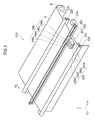
- Fig. 3 is a schematic view illustrating a structure of the image forming portion 210.
- the image forming portion 210 with a function of a so-called printer is housed in the housing 120 and is configured, for example, as follows.
- the image forming portion 210 includes a roll sheet R, sheet conveyor rollers 220, and a printer head 230.
- the printer head 230 includes, for example, ink tanks 240 (240c, 240m, 240y, and 240k) with cyan C, magenta M, yellow Y, and black K inks and discharge heads 250 (250c, 250m, 250y, and 250k) arranged on the ink tanks 240, respectively.
- the image forming portion 210 also includes a printer head slide shaft 260, a printer head drive motor 270, and a belt 280 attached to the printer head 230.
- the image forming portion 210 further includes a sheet discharge opening 290 from which a printed sheet S is discharged, and a sheet recovery unit 160.
- the sheet S as one end of the continuous roll sheet R is placed between the sheet conveyor rollers 220 rotated and driven by the driving mechanism and is conveyed in a conveyance direction F2 to a printing position.
- the printer head drive motor 270 mechanically moves the belt 280, and the printer head 230 moves in the printing direction (X direction) along the printer head slide shaft 260 to print the image on the sheet S based on the electric signal.
- the operation is repeated until the printing is finished, and the printed sheet S is cut in the X direction.
- the cut sheet S is discharged from the sheet discharge opening 290 by the sheet conveyor rollers 220.
- the sheet recovery unit 160 disposed below the housing 120 recovers the sheet S discharged from the sheet discharge opening 290.
- the type can be any type, such as an electrophotographic type, a thermal transfer type, and a dot impact type.
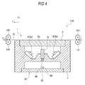
- Fig. 4 is a sectional view illustrating a configuration of part of the image reading portion 110 including the image sensor unit 1.
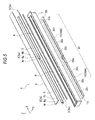
- Fig. 5 is a schematic exploded perspective view of the image sensor unit 1.
- the image sensor unit 1 includes a cover glass 2, light sources 3, rod-lens arrays 6 as light condensers, sensor substrate unit 91, a frame 7 as a supporting body that houses these components, and the like.
- the cover glass 2 and the frame 7 of the constituent members are formed long in the main-scan direction to handle the read length of the large original D.
- the frame 7 houses the constituent members of the image sensor unit 1.
- the frame 7 is rectangular, and a plurality of projections and recesses are formed inside to position and support the constituent members of the image sensor unit 1.
- the frame 7 is formed by a light-blocking resin material that is colored in black, for example. Polycarbonate can be applied as the resin material, for example.
- the cover glass 2 prevents dust from entering the frame 7.
- the cover glass 2 is planar and fixed on an upper part of the frame 7.
- the cover glass 2 is not essential in the present invention and can be omitted, it is desirable to set the cover glass 2 to protect the image sensor unit 1 from entrance of dust or scratches.
- the cover glass 2 is not limited to glass, and for example, a member formed by applying hard coating as necessary on the surface of a transparent resin material, such as an acrylic resin and polycarbonate, can be applied.
- each light source 3 includes, for example: light emitting elements 4r, 4g, and 4b with wavelengths of three colors of red R, green G, and blue B; and a substrate 5 for mounting the light emitting elements 4r, 4g, and 4b.
- the light emitting elements 4r, 4g, and 4b are, for example, LED chips and are mounted at predetermined intervals in a predetermined order on the substrate 5 formed long in the main-scan direction.
- the light sources 3a and 3b of the present embodiment include a plurality of substrates arranged in the main-scan direction, the substrates used in an image sensor unit that reads normal sized originals (for example, A4 and A3 sizes).
- the rod-lens array 6 is an optical member for focusing the reflected light from the original D on the sensor chip 30 mounted on a substrate body 14 or 19 of the sensor substrate 10.
- the rod-lens array 6 is disposed at a center position of the light source 3a and the light source 3b.
- the sensor chip 30 is positioned on an extension of an optical axis (alternate long and short dash line illustrated in Fig. 4 ) formed between an incident surface 6a and an emission surface 6b of the rod-lens array 6.
- the rod-lens array 6 includes a plurality of imaging elements (rod-lenses) of an erect equal magnification imaging type arranged in the main-scan direction.
- the rod-lens arrays 6 of the present embodiment are formed by arranging a plurality of rod-lens arrays in the main-scan direction, the arrays used in an image sensor unit that reads normal sized originals.
- Optical members with various well-known light condensing functions such as various micro-lens arrays, can be applied as the light condensers.
- the sensor substrate unit 91 includes a plurality of sensor substrates 10.
- the sensor substrate 10 includes the substrate bodies 14 and 19 and a plurality of sensor chips 30, the sensor chips 30 converting the reflected light focused by the rod-lens array 6 to electric signals.
- the plurality of sensor chips 30 are mounted on the substrate bodies 14 and 19 in the main-scan direction (longitudinal direction).
- the sensor substrate unit 91 is fixed under the frame 7.
- a plurality of sensor substrates 10 in a normal size are arranged and connected in the main-scan direction to form the sensor substrate unit 91 of the present embodiment at a predetermined read length. In this case, the sensor substrates 10 can be connected by a method described later to prevent damage of the sensor chips 30.
- the image reading portion 110 When the MFP 100 including the image sensor unit 1 configured as described above reads the original D, the image reading portion 110 successively activates the light emitting elements 4r, 4g, and 4b of the light sources 3a and 3b of the image sensor unit 1 to emit light on the original D conveyed by the original conveyor rollers 101 in a conveyance direction F1 at a predetermined conveyance speed.
- the light emitted from the light sources 3a and 3b is directed to the reading surface of the original D from two directions across the rod-lens array 6 to linearly and uniformly radiate the light throughout the main-scan direction.
- the original D reflects the radiated light to focus the light on photodiodes 31 described later of the sensor chips 30 through the rod-lens arrays 6.
- the sensor chips 30 convert the focused reflected light to electric signals, and a signal processing unit (not shown) processes the electric signals.
- the image reading portion 110 reads the reflected light of R, G, and B of one scan line to complete the reading operation of one scan line in the main-scan direction of the original D. After the end of the reading operation of one scan line, a reading operation of the next one scan line is performed in the same way as the operation described above along with the movement of the original D in the sub-scan direction. In this way, the image reading portion 110 repeats the reading operation of one scan line, while conveying the original D in the conveyance direction F1, to read the image of the entire surface of the original D.
- a configuration of the sensor substrate unit 91 will be described. The following description is about connection of two sensor substrates 10 in a line in the main-scan direction.
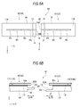
- Fig. 6A is a plan view of the sensor substrate unit 91.
- Fig. 6B is a view from an arrow A direction of Fig. 6A .
- the substrate body 14 of the sensor substrate 10A and the substrate body 19 of the sensor substrate 10B are formed in rectangular planar shapes long in the main-scan direction.
- ceramic substrates or glass epoxy substrates can be used as the substrate bodies 14 and 19.
- a plurality of (four each in Fig. 6A ) sensor chips 30 (30 1 to 30 4 and 30 5 to 30 8 ) are mounted on mounting surfaces 11A and 11B of the substrate bodies 14 and 19, the sensor chips 30 arranged in a line in the main-scan direction (longitudinal direction). As shown in Fig. 6B , the sensor chips 30 (30 1 to 30 8 ) are fixed on the mounting surfaces 11A and 11B by, for example, a thermosetting adhesive 12.
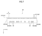
- Fig. 7 is a plan view illustrating a configuration of the sensor chip 30.
- the sensor chip 30 includes a plurality of photodiodes 31 as light receiving elements, a plurality of pads 32, circuit patterns (not shown), and the like.
- the photodiodes 31 play a role to detect the reflected light and are arranged in a line in the main-scan direction at equal pitches p.
- the photodiodes 31 are arranged throughout the whole length in the main-scan direction of the sensor chip 30. That is, the photodiodes 31A and 31B positioned at left and right edges of the sensor chip 30 are brought into close contact with farthest tips 33 (33A and 33B) in the main-scan direction of the sensor chip 30.
- the pads 32 play various roles, beginning with input/output pads 32A and 32B that input and output a start signal for detecting the reflected light.
- the input/output pads 32A and 32B are connected to the input/output pads 32A and 32B of the adjacent sensor chip 30 by wire bonding through thin metallic wires.
- the connection may be through the circuit patterns (not shown) on the substrate bodies 14 and 19.
- the start signal of the first sensor chip 30 of each sensor substrate is input from the outside.
- the input/output pads 32A and 32B are disposed farther from the farthest tips 33A and 33B of the sensor chip 30 compared to the photodiodes 31A and 31B.
- the circuit patterns of an analog output circuit, a shift register, and the like (not shown) on the sensor chip 30 and desired circuit patterns (not shown) on the substrate bodies 14 and 19 are connected by thin metallic wires through the pads 32.
- a "right side” denotes the side closer to the sensor substrate 10B in the main-scan direction
- a “left side” denotes the side closer to the sensor substrate 10A in the main-scan direction.
- the sensor substrate 10A will be described first.
- the substrate body 14 of the sensor substrate 10A is provided with an edge 13 on the right side that is the side connected to the sensor substrate 10B.
- the edge 13 is formed to protrude from the right side of the substrate body 14.
- the edge 13 is thinner than the thickness of the substrate body 14.
- the edge 13 protrudes from a middle portion in the thickness direction (Z direction) of the substrate body 14 toward the sensor substrate 10B, parallel to the mounting surface 11A of the substrate body 14.
- a tip on the right side of the edge 13 is a farthest edge 15 positioned at the extreme right of the sensor substrate 10A.
- An amount of protrusion of the edge 13, that is, a distance L1A (see Fig. 6B ) from a base end 16 of the edge 13 to the farthest edge 15, is the same as an amount of protrusion of an edge 18 of the substrate body 19 described later.
- a mounting position of the sensor chip 30 relative to the substrate body 14 will be described.
- the sensor chip 30 4 that may affect the pixel missing and that may be damaged, that is, the sensor chip 30 4 close to the side of the adjacent sensor substrate 10B, will be described.
- the farthest tip 33B on the right side is positioned inside (left side) of the farthest edge 15 of the sensor substrate 10A described above in the main-scan direction and is positioned and fixed outside (right side) beyond the base end 16 of the edge 13 in the main-scan direction.
- the right side (section including at least the farthest tip 33B) of the sensor chip 30 4 does not touch the edge 13, and the sensor chip 30 4 and the edge 13 are separated in the thickness direction of the substrate body 14.
- the width dimension (sub-scan direction) of the edge 13 is greater than the width dimension (sub-scan direction) of the sensor chip 30 4 .
- the width dimension of the edge 13 is the same as the width dimension of the substrate body 14.
- the farthest tip 33B of the sensor chip 30 4 is positioned inside of the farthest edge 15 of the sensor substrate 10A in the main-scan direction (longitudinal direction). Therefore, even if an obstacle touches the sensor substrate 10A during handling or storage, the edge 13 touches the obstacle first rather than the sensor chip 30 4 . As a result, the sensor chip 30 4 can be protected, and the damage can be prevented.
- the farthest tip 33B of the sensor chip 30 4 overlaps with the edge 13 in the thickness direction of the substrate body 14, in plan view of the sensor chip 30 4 as shown in Fig. 6A . Therefore, when the sensor substrate 10A and an obstacle come into contact during handling or storage, the edge 13 can be brought into touch with the obstacle first rather than the sensor chip 30 4 . As a result, the effect of preventing damage can be further improved.
- the width dimension of the edge 13 is greater than the width dimension of the sensor chip 30 4 , the farthest tip 33B of the sensor chip 30 4 is surrounded by the edge 13 in plan view. Therefore, the effect of preventing damage can be further improved.
- the sensor substrate 10B will be described.
- the substrate body 19 of the sensor substrate 10B is provided with the edge 18 on the left side that is the side connected to the sensor substrate 10A.
- the edge 18 is formed to protrude from the left side of the substrate body 19.
- the edge 18 is thinner than the thickness of the substrate body 19.
- the edge 18 protrudes from the bottom in the thickness direction (Z direction) of the substrate body 19 toward the sensor substrate 10A, parallel to the mounting surface 11B of the substrate body 19.
- the edge 18 protrudes at a position shifted from the aforementioned substrate body 19 in the thickness direction.
- a tip on the left side of the edge 18 is a farthest edge 20 positioned at the extreme left of the sensor substrate 10B.
- An amount of protrusion of the edge 18, that is, a distance L1B (see Fig. 6B ) from a base end 21 of the edge 18 to the farthest edge 20, is the same as the amount of protrusion L1A of the edge 13 of the adjacent substrate body 14.
- a mounting position of the sensor chip 30 relative to the substrate body 19 will be described.
- the sensor chip 30 5 that may affect the pixel missing and that may be damaged, that is, the sensor chip 30 5 close to the side of the adjacent sensor substrate 10A, will be described.
- the farthest tip 33A on the left side is positioned inside (right side) of the farthest edge 20 of the sensor substrate 10B described above in the main-scan direction and is positioned and fixed outside (left side) beyond the base end 21 of the edge 18 in the main-scan direction.
- the left side (section including at least the farthest tip 33A) of the sensor chip 30 5 does not touch the edge 18, and the sensor chip 30 5 and the edge 18 are separated in the thickness direction of the substrate body 19.
- the width dimension (sub-scan direction) of the edge 18 is greater than the width dimension (sub-scan direction) of the sensor chip 30 5 .
- the width dimension of the edge 18 is the same as the width dimension of the substrate body 19.
- the farthest tip 33A of the sensor chip 30 5 is positioned inside of the farthest edge 20 of the sensor substrate 10B in the main-scan direction (longitudinal direction). Therefore, even if an obstacle touches the sensor substrate 10B during handling or storage, the edge 18 touches the obstacle first rather than the sensor chip 30 5 . As a result, the sensor chip 30 5 can be protected, and the damage can be prevented.
- the farthest tip 33A of the sensor chip 30 5 overlaps with the edge 18 in the thickness direction of the substrate body 19, in plan view of the sensor chip 30 5 as shown in Fig. 6B . Therefore, when the sensor substrate 10B and an obstacle come into contact during handling or storage, the edge 18 can be brought into touch with the obstacle first rather than the sensor chip 30 5 . As a result, the effect of preventing damage can be further improved.
- the width dimension of the edge 18 is greater than the width dimension of the sensor chip 30 5 , the farthest tip 33A of the sensor chip 30 5 is surrounded by the edge 18 in plan view. Therefore, the effect of preventing damage can be further improved.
- a method of connecting the sensor substrates 10A and 10B will be described. There is a method in which an assembly worker uses a metallurgical microscope or a stereoscopic microscope to observe and connect the sensor substrates 10A and 10B. Hereinafter, a case in which the assembly worker uses a metallurgical microscope to observe and connect the sensor substrates 10A and 10B will be described.
- the assembly worker manufactures in advance the sensor substrates 10A and 10B on which the sensor chips 30 1 to 30 4 and 30 5 to 30 8 are mounted.
- the assembly worker uses a holder to hold the sensor substrates 10A and 10B so that the edge 13 of the sensor substrate 10A and the edge 18 of the sensor substrate 10B face each other as shown in Figs. 6A and 6B .
- the assembly worker makes an adjustment so that the sensor chips 30 1 to 30 4 of the sensor substrate 10A and the sensor chips 30 5 to 30 8 of the sensor substrate 10B form a line.
- the assembly worker moves the holder to gradually bring the sensor substrates 10A and 10B closer while maintaining the sensor chips 30 1 to 30 4 and the sensor chips 30 5 to 30 8 to form a line.
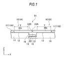
- Figs. 8A and 1 are diagrams illustrating a state that the sensor substrates 10A and 10B are brought into close contact.
- Fig. 8A is a plan view of the sensor substrate unit 91.
- Fig. 1 is a view from an arrow B direction illustrated in Fig. 8A .
- the edge 13 of the sensor substrate 10A and the edge 18 of the sensor substrate 10B overlap in the thickness direction without touching.
- the substrate bodies 14 and 19 do not touch each other below the area where the sensor chip 30 4 and the sensor chip 30 5 face each other, and a space 23 is formed.
- Fig. 8B is an enlarged view of a boundary section between the sensor substrate 10A and the sensor substrate 10B of Fig. 8A .
- the assembly worker adjusts the interval between the photodiode 31B of the sensor chip 30 4 of the sensor substrate 10A and the photodiode 31A of the sensor chip 30 5 of the sensor substrate 10B to be the same distance as the pitch p of the photodiodes 31.
- the farthest tip 33B of the sensor chip 30 4 is positioned outside of the base end 16 of the edge 13, and the farthest tip 33A of the sensor chip 30 5 is positioned outside of the base end 21 of the edge 18.
- the farthest tip 33B of the sensor chip 30 4 and the edge 13 are separated in the thickness direction of the substrate body 14, and the farthest tip 33A of the sensor chip 30 5 and the edge 18 are separated in the thickness direction of the substrate body 19. Therefore, other than the sensor chips 30, there is no obstacle that touches the sensor chips 30 at the nearest surrounding of the farthest tip 33B of the sensor chip 30 4 and the nearest surrounding of the farthest tip 33A of the sensor chip 30 5 . As a result, the intervals of the sensor chips 30 can be accurately determined without being inhibited by obstacles.
- the interval between the photodiode 31B of the sensor chip 30 4 and the photodiode 31A of the sensor chip 30 5 may not be the same distance as the pitch p and may be a distance greater than the pitch p if the distance is a predetermined distance. More specifically, as long as the interval between the photodiode 31B of the sensor chip 30 4 and the photodiode 31A of the sensor chip 30 5 is a predetermined distance, the image can be interpolated based on the predetermined distance after the image is read by the image sensor unit 1.
- a gap (distance q shown in Fig. 8B ) between the farthest tip 33B of the sensor chip 30 4 and the farthest tip 33A of the sensor chip 30 5 .
- the distance q of the gap is set to be smaller than a distance (distance r shown in Fig. 8B ) between the farthest edge 15 and the base end 21 and smaller than a distance (distance s shown in Fig. 8B ) between the farthest edge 20 and the base end 16.
- the contact of the farthest edge 15 with the base end 21 can be prevented before the distance between the photodiode 31B of the sensor chip 30 4 and the photodiode 31A of the sensor chip 30 5 is adjusted to the pitch p or the predetermined distance.
- the contact of the farthest edge 20 with the base end 16 before the distance between the photodiode 31B of the sensor chip 30 4 and the photodiode 31A of the sensor chip 30 5 is adjusted to the pitch p or the predetermined distance can be prevented.
- Fig. 9A is a plan view illustrating a state that the sensor substrates 10A and 10B are fixed by the fixation members 26.
- Fig. 9B is a sectional view of a I-I line shown in Fig. 9A .
- the fixation members 26 of the present embodiment are formed in a rectangular planar shape and are fixed at two sections on both sides of the sensor substrates 10A and 10B in the sub-scan direction (width direction). Specifically, the fixation members 26 are fixed across the mounting surface 11A of the substrate body 14 and the mounting surface 11B of the substrate body 19. Screws 28 are used to fix the fixation members 26 on the mounting surfaces 11A and 11B. Therefore, the fixation members 26 connect the sensor substrates 10, while the distance between the sensor substrates 10 is held.
- an abutment surface 27 of the fixation member 26 abutted with the mounting surface 11A of the substrate body 14 and the mounting surface 11B of the substrate body 19 is formed in a flat surface. Therefore, the mounting surface 11A of the substrate body 14 and the mounting surface 11B of the substrate body 19 can be held in a flush state, and the sensor chips 30 1 to 30 8 mounted on the mounting surfaces 11A and 11B can also be held in a flush state.
- the fixation members 26 are at least formed by a material with a coefficient of linear expansion lower than that of the substrate bodies 14 and 19. Since the fixation members 26 are fixed to the mounting surface 11A of the substrate body 14 and the mounting surface 11B of the substrate body 19, expansion and contraction of the fixation members 26 may affect the distance between the photodiode 31B of the sensor chip 30 4 and the photodiode 31A of the sensor chip 30 5 . Therefore, the fixation members 26 can be formed by a material with a coefficient of linear expansion lower than that of the material of the substrate bodies 14 and 19 to reduce the change in the distance between the photodiodes 31B and 31A. More specifically, even if the temperature of the storage location drops when the image sensor unit 1 is stored without being used, the contact of the sensor chips 30 4 and 30 5 can be prevented by reducing the contraction of the fixation members 26 in the main-scan direction.
- a space 23 is formed below the section where the sensor chips 30 4 and 30 5 face each other. Therefore, even if the flush state cannot be maintained between the sensor chips 30 4 and 30 5 and there is a difference in level in the direction orthogonal to the mounting surface 11, the formation of the space 29 can prevent the sensor chip 30 in the lower level from touching the mounting surface 11 of the sensor substrate 10.
- the assembly worker uses thin metallic wires to electrically connect, by wire bonding, the input/output pad 32B of the sensor chip 30 4 of the sensor substrate 10A and the input/output pad 32A of the sensor chip 30 5 of the sensor substrate 10B.
- the adhesive 12 and the substrate bodies 14 and 19 can support the force, and the load on the sensor chips 30 4 and 30 5 can be reduced. Therefore, when the sensor chips 30 4 and 30 5 are mounted on the substrate bodies 14 and 19, the input/output pads 32A and 32B are fixed at positions within a range (area T shown in Fig. 1 ) where the adhesive 12 is applied.
- the electric connection by wire bonding using the thin metallic wires may be performed just after the mounting of the sensor chips 30 1 to 30 4 and 30 5 to 30 8 on the substrate bodies 14 and 19 by the assembly worker.
- the assembly worker incorporates the sensor substrate unit 91 connected with sensor substrates 10A and 10B into the frame 7 shown in Fig. 5 to fix the sensor substrates 10A and 10B to the frame 7 by screws or adhesive to manufacture the image sensor unit 1.
- the pitch p or the predetermined distance is maintained between the sensor chips 30 4 and 30 5 in the manufactured image sensor unit 1 as described above, and the image can be read without missing pixels.
- the farthest tips 33B and 33A of the sensor chips 30 4 and 30 5 mounted on the substrate bodies 14 and 19 of the sensor substrates 10A and 10B are positioned inside of the farthest edges 15 and 20 of the edges 13 and 18 of the substrate bodies 14 and 19 in a longitudinal direction in the present embodiment. Therefore, even if an obstacle touches the sensor substrates 10A and 10B during handling or storage, the obstacle touches the edges 13 and 18 rather than the sensor chips 30 4 and 30 5 . As a result, the sensor chips 30 4 and 30 5 can be protected, and the damage can be prevented.
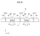
- Fig. 10 is a plan view illustrating configurations of the sensor substrate unit 92 according to the present embodiment.
- a plurality of (e.g. four each) sensor chips 50 (50 1 to 50 4 , 50 5 to 50 8 , and 50 9 to 50 12 ) are mounted on the mounting surfaces of the respective substrate bodies of the sensor substrates 40A, 40B, and 40C, and the sensor chips 50 are linearly arranged in the main-scan direction (longitudinal direction).
- Fig. 10 50 2 , 50 3 , 50 6 , 50 7 , 50 10 , and 50 11 will be omitted.
- the sensor substrate 40A of the three sensor substrates has similar components to those of the sensor substrate 10A of the first embodiment.
- the sensor substrate 40B has combined components of the sensor substrate 10A and the sensor substrate 10B of the first embodiment.
- the sensor substrate 40C has similar components to those of the sensor substrate 10B of the first embodiment.
- the similar components to those of the first embodiment are designated with the same reference numerals in Fig. 10 .
- the edge 13 is formed on the right side of the substrate body of the sensor substrate 40A, and the edge 18 is formed on the left side of the substrate body of the sensor substrate 40B.
- the edge 13 is formed on the right side of the substrate body of the sensor substrate 40B, and the edge 18 is formed on the left side of the substrate body of the sensor substrate 40C.
- the farthest tips 33B of the sensor chips 50 4 and 50 8 mounted on the substrate bodies of the sensor substrates 40A and 40B are positioned inside of the farthest edges 15 of the edges 13 in the main-scan direction.
- the farthest tips 33A of the sensor chips 50 5 and 50 9 mounted on the substrate bodies of the sensor substrates 40B and 40C are positioned inside of the farthest edges 20 of the edges 18 in the main-scan direction.
- the obstacle first touches the edges 13 and 18 rather than the sensor chips 50 4 , 50 5 , 50 8 , and 50 9 .
- the sensor chips 50 4 , 50 5 , 50 8 , and 50 9 can be protected, and the damage can be prevented.
- the assembly method of the sensor substrates 40A, 40B, and 40C is similar to that of the first embodiment, and the description will not be repeated.
- the edges 13 and 18 may be line-symmetric to a center line C shown in Fig. 10 in the three sensor substrates 40A, 40B, and 40C.
- the case of connecting the three sensor substrates 40A, 40B, and 40C has been described, the case is not limited to this. A case of connecting four or more sensor substrates can be similarly applied.
- the image reading apparatus is not limited to the sheet-feed type image scanner, and a flat-bed type image scanner can also be similarly applied.
- Fig. 11 is a plan view of sensor substrate unit 93 according to another embodiment.
- a plurality of (four each in Fig. 11 ) sensor chips 70 (70 1 to 70 4 , 70 5 to 70 8 , and 70 9 to 70 12 ) are mounted on mounting surfaces of substrate bodies of sensor substrates 60A, 60B, and 60C.
- the individual sensor chips 70 1 to 70 4 mounted on the substrate body of the sensor substrate 60A are alternately shifted in the width direction to form a staggered arrangement.
- the individual sensor chips 70 5 to 70 8 and 70 9 to 70 12 of the substrate bodies of the sensor substrates 60B and 60C are similarly arranged in the staggered manner.
- the arrangement in a line is not limited to the arrangement in a straight line, and the arrangement in a staggered manner that can be approximated to the arrangement in a line is also included.
- the sensor chips 30 1 to 30 4 and 30 5 to 30 8 (sensor chips 50 1 to 50 4 , 50 5 to 50 8 , and 50 9 to 50 12 ) form a line, specifically, a straight line.
- the arrangement is not limited to this, and a case of connecting the sensor substrates so that the sensor chips are arranged in a staggered manner when a plurality of sensor chips on the substrate body are seen as one sensor chip can also be similarly applied.
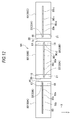
- Fig. 12 is a plan view of sensor substrate unit 94 of another embodiment.
- a plurality of (four each in Fig. 12 ) sensor chips 90 (90 1 to 90 4 , 90 5 to 90 8 , 90 9 to 90 12 ) are mounted on mounting surfaces of substrate bodies of sensor substrates 80A, 80B, and 80C, the sensor chips 90 arranged in a straight line.
- the sensor chips 90 1 to 90 4 mounted on the substrate body of the sensor substrate 80A and the sensor chips 90 5 to 90 8 mounted on the sensor substrate 80B are shifted in the sub-scan direction.
- the sensor chips 90 5 to 90 8 mounted on the substrate body of the sensor substrate 80B and the sensor chips 90 9 to 90 12 mounted on the substrate body of the sensor substrate 80C are shifted in the sub-scan direction. Therefore, the sensor substrates 80A, 80B, and 80C are connected so that the sensor chips are arranged in a staggered manner when the sensor chips 90 1 to 90 4 , 90 5 to 90 8 , and 90 9 to 90 12 are seen as one sensor chip each.
- the image sensor unit, the image reading apparatus, and the image forming apparatus according to the present invention are to prevent damage to sensor chips.
- a plurality of edges of sensor substrates are connected in a longitudinal direction in a sensor substrate unit. Farthest tips of sensor chips at the edges of the sensor substrates are positioned inside of farthest edges of the edges in the longitudinal direction. The edges of the connected sensor substrates overlap each other in a thickness direction of the sensor substrates in plan view.
Landscapes
- Engineering & Computer Science (AREA)
- Multimedia (AREA)
- Signal Processing (AREA)
- Facsimile Heads (AREA)
- Facsimile Scanning Arrangements (AREA)
- Solid State Image Pick-Up Elements (AREA)
- Image Input (AREA)
Applications Claiming Priority (1)
| Application Number | Priority Date | Filing Date | Title |
|---|---|---|---|
| JP2013128739A JP2015005827A (ja) | 2013-06-19 | 2013-06-19 | イメージセンサユニット、画像読取装置および画像形成装置 |
Publications (1)
| Publication Number | Publication Date |
|---|---|
| EP2816793A1 true EP2816793A1 (de) | 2014-12-24 |
Family
ID=50897372
Family Applications (1)
| Application Number | Title | Priority Date | Filing Date |
|---|---|---|---|
| EP14170167.2A Withdrawn EP2816793A1 (de) | 2013-06-19 | 2014-05-28 | Bildsensoreinheit, Bildlesevorrichtung und Bilderzeugungsvorrichtung |
Country Status (4)
| Country | Link |
|---|---|
| US (1) | US9100524B2 (de) |
| EP (1) | EP2816793A1 (de) |
| JP (1) | JP2015005827A (de) |
| CN (1) | CN104243756A (de) |
Cited By (1)
| Publication number | Priority date | Publication date | Assignee | Title |
|---|---|---|---|---|
| WO2017080904A1 (de) * | 2015-11-11 | 2017-05-18 | Protechna Herbst Gmbh & Co. Kg | Vorrichtung und verfahren zur überwachung einer laufenden warenbahn |
Families Citing this family (5)
| Publication number | Priority date | Publication date | Assignee | Title |
|---|---|---|---|---|
| JP2017092383A (ja) * | 2015-11-16 | 2017-05-25 | 日本電気株式会社 | 固体撮像ユニット、及び、これを用いた固体撮像装置 |
| JP6214836B1 (ja) | 2015-12-16 | 2017-10-18 | 三菱電機株式会社 | 受光ユニット及びイメージセンサ |
| CN108124075B (zh) * | 2017-11-15 | 2024-07-02 | 威海华菱光电股份有限公司 | 图像传感器 |
| US10944882B2 (en) | 2017-12-01 | 2021-03-09 | Hewlett-Packard Development Company, L.P. | Image sensor line orientation |
| DE112020004285T5 (de) * | 2019-09-11 | 2022-06-23 | Mitsubishi Electric Corporation | Bildlesevorrichtung |
Citations (7)
| Publication number | Priority date | Publication date | Assignee | Title |
|---|---|---|---|---|
| JPH0786541A (ja) | 1993-09-16 | 1995-03-31 | Rohm Co Ltd | 光電変換装置 |
| EP0751568A2 (de) * | 1995-05-31 | 1997-01-02 | Nippon Seiki Co., Ltd. | Bestücken von lichtemittierenden Vorrichtungen und Herstellungsverfahren |
| US5594260A (en) * | 1993-09-03 | 1997-01-14 | Rohm Co., Ltd. | Photoelectric converter with photoelectric conversion devices mounted separately from wiring boards |
| EP1650949A1 (de) * | 2004-10-25 | 2006-04-26 | Seiko Instruments Inc. | Vorlagenlesegerät, Bilderzeugungsgerät und Bildabtaster |
| US20100213355A1 (en) * | 2009-02-25 | 2010-08-26 | Weng-Lyang Wang | Full-width Line Image-sensing Head |
| EP2608519A2 (de) * | 2011-12-22 | 2013-06-26 | Canon Components, Inc. | Bildsensoreinheit, Bildlesevorrichtung und Bilderzeugungsvorrichtung |
| EP2608518A2 (de) * | 2011-12-22 | 2013-06-26 | Canon Components, Inc. | Bildsensoreinheit, Bildlesevorrichtung und Bilderzeugungsvorrichtung |
Family Cites Families (2)
| Publication number | Priority date | Publication date | Assignee | Title |
|---|---|---|---|---|
| JP4332374B2 (ja) * | 2003-06-17 | 2009-09-16 | キヤノン株式会社 | 画像読み取り装置 |
| CN2854956Y (zh) * | 2005-11-22 | 2007-01-03 | 威海华菱光电有限公司 | 接触式图像传感器(1) |
-
2013
- 2013-06-19 JP JP2013128739A patent/JP2015005827A/ja active Pending
-
2014
- 2014-05-21 US US14/283,309 patent/US9100524B2/en active Active
- 2014-05-28 EP EP14170167.2A patent/EP2816793A1/de not_active Withdrawn
- 2014-06-19 CN CN201410276957.9A patent/CN104243756A/zh active Pending
Patent Citations (7)
| Publication number | Priority date | Publication date | Assignee | Title |
|---|---|---|---|---|
| US5594260A (en) * | 1993-09-03 | 1997-01-14 | Rohm Co., Ltd. | Photoelectric converter with photoelectric conversion devices mounted separately from wiring boards |
| JPH0786541A (ja) | 1993-09-16 | 1995-03-31 | Rohm Co Ltd | 光電変換装置 |
| EP0751568A2 (de) * | 1995-05-31 | 1997-01-02 | Nippon Seiki Co., Ltd. | Bestücken von lichtemittierenden Vorrichtungen und Herstellungsverfahren |
| EP1650949A1 (de) * | 2004-10-25 | 2006-04-26 | Seiko Instruments Inc. | Vorlagenlesegerät, Bilderzeugungsgerät und Bildabtaster |
| US20100213355A1 (en) * | 2009-02-25 | 2010-08-26 | Weng-Lyang Wang | Full-width Line Image-sensing Head |
| EP2608519A2 (de) * | 2011-12-22 | 2013-06-26 | Canon Components, Inc. | Bildsensoreinheit, Bildlesevorrichtung und Bilderzeugungsvorrichtung |
| EP2608518A2 (de) * | 2011-12-22 | 2013-06-26 | Canon Components, Inc. | Bildsensoreinheit, Bildlesevorrichtung und Bilderzeugungsvorrichtung |
Cited By (1)
| Publication number | Priority date | Publication date | Assignee | Title |
|---|---|---|---|---|
| WO2017080904A1 (de) * | 2015-11-11 | 2017-05-18 | Protechna Herbst Gmbh & Co. Kg | Vorrichtung und verfahren zur überwachung einer laufenden warenbahn |
Also Published As
| Publication number | Publication date |
|---|---|
| CN104243756A (zh) | 2014-12-24 |
| JP2015005827A (ja) | 2015-01-08 |
| US9100524B2 (en) | 2015-08-04 |
| US20140376061A1 (en) | 2014-12-25 |
Similar Documents
| Publication | Publication Date | Title |
|---|---|---|
| US8848209B2 (en) | Image sensor unit, image reading apparatus, and image forming apparatus | |
| US9059367B2 (en) | Image sensor unit, image reading apparatus, image forming apparatus, and manufacturing method | |
| US9065959B2 (en) | Image sensor unit, image reading apparatus, and image forming apparatus | |
| US9100524B2 (en) | Image sensor unit, image reading apparatus, and image forming apparatus | |
| US9571689B2 (en) | Image sensor unit, image reading apparatus, and image forming apparatus | |
| US9158062B2 (en) | Illumination apparatus, image sensor unit, and image reading apparatus | |
| US9065961B2 (en) | Image sensor unit, image reading apparatus, and image forming apparatus | |
| JP3507284B2 (ja) | ロッドレンズアレイ及び密着型イメージセンサ及び画像読取装置 | |
| US9247095B2 (en) | Image sensor unit, image reading apparatus, and image forming apparatus | |
| JP7133681B2 (ja) | 照明装置、センサユニット、読取装置および画像形成装置 | |
| JP4206992B2 (ja) | 撮像ユニット及び画像読取装置 | |
| US7894105B2 (en) | Image reading unit and image reader | |
| US10091382B2 (en) | Illumination apparatus and sensor unit | |
| JP5734470B2 (ja) | イメージセンサユニット、画像読取装置および画像形成装置 | |
| US10136019B2 (en) | Illumination apparatus, sensor unit, and reading apparatus | |
| US10323825B2 (en) | Light guide, illumination device, sensor unit, reading apparatus, image forming apparatus, and paper sheet distinguishing apparatus | |
| JP2015195152A (ja) | 照明装置、イメージセンサユニット、画像読取装置および画像形成装置 | |
| JP2015128247A (ja) | イメージセンサユニット、画像読取装置および画像形成装置 | |
| JP2017175289A (ja) | 照明装置、イメージセンサユニット、画像読取装置および画像形成装置 |
Legal Events
| Date | Code | Title | Description |
|---|---|---|---|
| PUAI | Public reference made under article 153(3) epc to a published international application that has entered the european phase |
Free format text: ORIGINAL CODE: 0009012 |
|
| 17P | Request for examination filed |
Effective date: 20140528 |
|
| AK | Designated contracting states |
Kind code of ref document: A1 Designated state(s): AL AT BE BG CH CY CZ DE DK EE ES FI FR GB GR HR HU IE IS IT LI LT LU LV MC MK MT NL NO PL PT RO RS SE SI SK SM TR |
|
| AX | Request for extension of the european patent |
Extension state: BA ME |
|
| R17P | Request for examination filed (corrected) |
Effective date: 20150615 |
|
| RBV | Designated contracting states (corrected) |
Designated state(s): AL AT BE BG CH CY CZ DE DK EE ES FI FR GB GR HR HU IE IS IT LI LT LU LV MC MK MT NL NO PL PT RO RS SE SI SK SM TR |
|
| STAA | Information on the status of an ep patent application or granted ep patent |
Free format text: STATUS: THE APPLICATION HAS BEEN WITHDRAWN |
|
| 18W | Application withdrawn |
Effective date: 20160518 |