EP2819155B1 - Dünnfilmtransistorarraysubstrat und herstellungsverfahren dafür - Google Patents
Dünnfilmtransistorarraysubstrat und herstellungsverfahren dafür Download PDFInfo
- Publication number
- EP2819155B1 EP2819155B1 EP12869085.6A EP12869085A EP2819155B1 EP 2819155 B1 EP2819155 B1 EP 2819155B1 EP 12869085 A EP12869085 A EP 12869085A EP 2819155 B1 EP2819155 B1 EP 2819155B1
- Authority
- EP
- European Patent Office
- Prior art keywords
- thin film
- layer thin
- gate
- source
- insulating layer
- Prior art date
- Legal status (The legal status is an assumption and is not a legal conclusion. Google has not performed a legal analysis and makes no representation as to the accuracy of the status listed.)
- Active
Links
Images

Classifications
-
- H—ELECTRICITY
- H10—SEMICONDUCTOR DEVICES; ELECTRIC SOLID-STATE DEVICES NOT OTHERWISE PROVIDED FOR
- H10D—INORGANIC ELECTRIC SEMICONDUCTOR DEVICES
- H10D86/00—Integrated devices formed in or on insulating or conducting substrates, e.g. formed in silicon-on-insulator [SOI] substrates or on stainless steel or glass substrates
- H10D86/01—Manufacture or treatment
- H10D86/021—Manufacture or treatment of multiple TFTs
- H10D86/0221—Manufacture or treatment of multiple TFTs comprising manufacture, treatment or patterning of TFT semiconductor bodies
-
- H—ELECTRICITY
- H10—SEMICONDUCTOR DEVICES; ELECTRIC SOLID-STATE DEVICES NOT OTHERWISE PROVIDED FOR
- H10D—INORGANIC ELECTRIC SEMICONDUCTOR DEVICES
- H10D30/00—Field-effect transistors [FET]
- H10D30/60—Insulated-gate field-effect transistors [IGFET]
- H10D30/67—Thin-film transistors [TFT]
- H10D30/6704—Thin-film transistors [TFT] having supplementary regions or layers in the thin films or in the insulated bulk substrates for controlling properties of the device
- H10D30/6713—Thin-film transistors [TFT] having supplementary regions or layers in the thin films or in the insulated bulk substrates for controlling properties of the device characterised by the properties of the source or drain regions, e.g. compositions or sectional shapes
-
- G—PHYSICS
- G02—OPTICS
- G02F—OPTICAL DEVICES OR ARRANGEMENTS FOR THE CONTROL OF LIGHT BY MODIFICATION OF THE OPTICAL PROPERTIES OF THE MEDIA OF THE ELEMENTS INVOLVED THEREIN; NON-LINEAR OPTICS; FREQUENCY-CHANGING OF LIGHT; OPTICAL LOGIC ELEMENTS; OPTICAL ANALOGUE/DIGITAL CONVERTERS
- G02F1/00—Devices or arrangements for the control of the intensity, colour, phase, polarisation or direction of light arriving from an independent light source, e.g. switching, gating or modulating; Non-linear optics
- G02F1/01—Devices or arrangements for the control of the intensity, colour, phase, polarisation or direction of light arriving from an independent light source, e.g. switching, gating or modulating; Non-linear optics for the control of the intensity, phase, polarisation or colour
- G02F1/13—Devices or arrangements for the control of the intensity, colour, phase, polarisation or direction of light arriving from an independent light source, e.g. switching, gating or modulating; Non-linear optics for the control of the intensity, phase, polarisation or colour based on liquid crystals, e.g. single liquid crystal display cells
- G02F1/133—Constructional arrangements; Operation of liquid crystal cells; Circuit arrangements
- G02F1/136—Liquid crystal cells structurally associated with a semi-conducting layer or substrate, e.g. cells forming part of an integrated circuit
- G02F1/1362—Active matrix addressed cells
- G02F1/136286—Wiring, e.g. gate line, drain line
-
- H—ELECTRICITY
- H10—SEMICONDUCTOR DEVICES; ELECTRIC SOLID-STATE DEVICES NOT OTHERWISE PROVIDED FOR
- H10D—INORGANIC ELECTRIC SEMICONDUCTOR DEVICES
- H10D30/00—Field-effect transistors [FET]
- H10D30/60—Insulated-gate field-effect transistors [IGFET]
- H10D30/67—Thin-film transistors [TFT]
- H10D30/6729—Thin-film transistors [TFT] characterised by the electrodes
-
- H—ELECTRICITY
- H10—SEMICONDUCTOR DEVICES; ELECTRIC SOLID-STATE DEVICES NOT OTHERWISE PROVIDED FOR
- H10D—INORGANIC ELECTRIC SEMICONDUCTOR DEVICES
- H10D86/00—Integrated devices formed in or on insulating or conducting substrates, e.g. formed in silicon-on-insulator [SOI] substrates or on stainless steel or glass substrates
- H10D86/01—Manufacture or treatment
- H10D86/021—Manufacture or treatment of multiple TFTs
- H10D86/0231—Manufacture or treatment of multiple TFTs using masks, e.g. half-tone masks
-
- H—ELECTRICITY
- H10—SEMICONDUCTOR DEVICES; ELECTRIC SOLID-STATE DEVICES NOT OTHERWISE PROVIDED FOR
- H10D—INORGANIC ELECTRIC SEMICONDUCTOR DEVICES
- H10D86/00—Integrated devices formed in or on insulating or conducting substrates, e.g. formed in silicon-on-insulator [SOI] substrates or on stainless steel or glass substrates
- H10D86/40—Integrated devices formed in or on insulating or conducting substrates, e.g. formed in silicon-on-insulator [SOI] substrates or on stainless steel or glass substrates characterised by multiple TFTs
- H10D86/421—Integrated devices formed in or on insulating or conducting substrates, e.g. formed in silicon-on-insulator [SOI] substrates or on stainless steel or glass substrates characterised by multiple TFTs having a particular composition, shape or crystalline structure of the active layer
- H10D86/423—Integrated devices formed in or on insulating or conducting substrates, e.g. formed in silicon-on-insulator [SOI] substrates or on stainless steel or glass substrates characterised by multiple TFTs having a particular composition, shape or crystalline structure of the active layer comprising semiconductor materials not belonging to the Group IV, e.g. InGaZnO
-
- H—ELECTRICITY
- H10—SEMICONDUCTOR DEVICES; ELECTRIC SOLID-STATE DEVICES NOT OTHERWISE PROVIDED FOR
- H10D—INORGANIC ELECTRIC SEMICONDUCTOR DEVICES
- H10D86/00—Integrated devices formed in or on insulating or conducting substrates, e.g. formed in silicon-on-insulator [SOI] substrates or on stainless steel or glass substrates
- H10D86/40—Integrated devices formed in or on insulating or conducting substrates, e.g. formed in silicon-on-insulator [SOI] substrates or on stainless steel or glass substrates characterised by multiple TFTs
- H10D86/441—Interconnections, e.g. scanning lines
-
- H—ELECTRICITY
- H10—SEMICONDUCTOR DEVICES; ELECTRIC SOLID-STATE DEVICES NOT OTHERWISE PROVIDED FOR
- H10D—INORGANIC ELECTRIC SEMICONDUCTOR DEVICES
- H10D86/00—Integrated devices formed in or on insulating or conducting substrates, e.g. formed in silicon-on-insulator [SOI] substrates or on stainless steel or glass substrates
- H10D86/40—Integrated devices formed in or on insulating or conducting substrates, e.g. formed in silicon-on-insulator [SOI] substrates or on stainless steel or glass substrates characterised by multiple TFTs
- H10D86/60—Integrated devices formed in or on insulating or conducting substrates, e.g. formed in silicon-on-insulator [SOI] substrates or on stainless steel or glass substrates characterised by multiple TFTs wherein the TFTs are in active matrices
Definitions
- the present invention relates to a thin film transistor array substrate and a manufacturing method thereof.
- AMLCD Active Matrix Liquid Crystal Display
- the band gap of the a-Si material is only 1.7eV, it is opaque to visible light and is photosensitive within the range of the visible light, thus an opaque metal mask plate (black matrix) needs to be added to shield the light, correspondingly the complexity of the production process of the TFT array substrate is increased, then the cost is increased and the reliability and opening rate are lowered. Meanwhile, to obtain enough brightness, the light strength of a light source needs to be enhanced, and correspondingly power consumption is increased. In addition, the mobility of the a-Si material can hardly exceed 1cm 2 ⁇ V -1 ⁇ s -1 , thus current TFT array substrates can hardly meet needs of liquid crystal televisions with a continuously increasing size and drive circuits with better performance.
- an oxide semiconductor TFT has been widely paid attention due to its various advantages and has been undergoing fast development during recent years.
- An oxide semiconductor being transparent and having a high mobility, fine uniformity and a simple fabrication process, can better meet needs of large- ⁇ sized liquid crystal displays.
- the production of the oxide TFT can satisfactorily match current LCD production lines, then the transition is easy, thus people have paid more attention to the oxide TFT which has been a hot research topic recently.
- the prior art need to use at least 4 masking exposing processes during manufacturing the oxide TFT array substrate, then the production process is very complex and the cost of the mask plate is high, correspondingly the production cost of the product is increased, the yield of the product is lowered, and equipment capacity is decreased.
- a TFT substrate comprises: a substrate; a first oxide layer formed above the substrate; a second oxide layer formed above the first oxide layer with a channel part interposed therebetween; a gate insulating film formed above the substrate, the first oxide layer and the second oxide layer; a gate electrode and a gate wire formed above the gate insulating film.
- US 2010/208153 A1 discloses a thin film transistor liquid crystal display (TFT-LCD) array substrate and a manufacturing method thereof.
- the TFT-LCD array substrate comprises a gate line and a data line that define a pixel region, wherein the pixel region is provided with a thin film transistor, a pixel electrode formed on the array substrate, and a storage electrode of transparent structure that overlaps with the pixel electrode and, together with the pixel electrode, constitutes a storage capacitor.
- EP 1 947 695 A2 discloses a manufacturing method of a thin film transistor array Substrate, comprising a plurality of pixel units, the method comprising: forming a channel region portion being an active layer thin film and a conductive layer thin film on a substrate, comprising: depositing an oxide thin film on the substrate, and conducting surface treatment to the oxide thin film so as to form a layer of conductive layer thin film on the surface of the oxide thin film; and the oxide thin film that has not been treated under the conductive layer thin film being the active layer thin film; wherein the active layer of the thin film transistor is located within the pixel unit and is distributed within the whole area of the pixel unit.
- the embodiment of the present invention provides a manufacturing method of the TFT array substrate, comprising following steps:
- the TFT array substrate is formed.
- the TFT array substrate is assembled to a liquid crystal display, one end of all the gate scanning lines is connected to a scan drive circuit through a pin, and one end of all the data lines is connected to a data drive circuit through the through hole.
- the drawings of the present invention mainly show the section views near the TFT. Therefore, the through hole for the connection between the data lines and the data drive circuit is not illustrated.
- the position of the through hole can be any position as in the prior art, and is not limited in the embodiments of the present invention.
- the TFT array substrate as formed can comprise a plurality of pixel units, and Fig. 1 is a top view of a pixel unit of the TFT array substrate, the horizontally arranged are the parallel gate scanning lines 20, the data lines 21 are arranged to cross with the gate scanning lines 20 (for example, perpendicular to each other), and the area separated by the gate scanning lines 20 and the data lines 21 is a pixel unit.
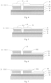
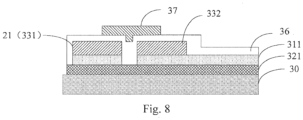
- the steps of manufacturing the TFT array substrate of the present invention with 3 mask plates will be detailed hereinafter in combination with Figs. 2-8 , the section view at position A-A' in Fig. 1 is to show the structure of the TFT device, in which the source electrode 331, the drain electrode 332 and the gate electrode 337 of the TFT device are illustrated, and the section view at position A-A' will be described in each step hereinafter.
- the substrate 30 provided for manufacturing the TFT array substrate can be quartz glass, ordinary glass, plastic substrate and etc.
- An oxide thin film is deposited on the substrate 30, methods such as magnetron sputtering can be used to deposit ZnO, In 2 O 3 , IGZO and etc., and the thickness of the deposited oxide thin film is, for example, 100-150nm; surface treatment is conducted to the oxide thin film, after the treatment a layer of conductive layer thin film 31 is formed on the surface of the oxide thin film, and the oxide thin film below the conductive layer thin film that has not been treated is the active layer thin film 32.
- the surface treatment can be methods such as ion implantation and plasma method.
- the method of ion implantation can be used to implant metal such as Al and In to the ZnO thin film, the metal Sn can be implanted into the In 2 O 3 thin film, of course, other metals can also be implanted.
- the plasma method can also be used to ionize H 2 or N 2 to plasma, and then the ZnO thin film, the IGZO thin film and etc. are treated.
- the thickness of the transparent conductive layer thin film 31 formed after the surface treatment is, for example, 50-100nm.
- the first masking process is a first masking process
- a gray tone or half tone mask plate (description is made hereinafter taking the gray tone mask plate as an example), that is, the first mask plate, is used to conduct exposing and developing to the photoresist.
- the positions corresponding to the data lines, the pixel electrode, the source electrode of the TFT and the channel are not exposed, the position corresponding to the drain electrode of the TFT is partially exposed, and the other positions are completely exposed, thus the conductive layer thin film and the source/drain electrode layer thin film are etched to obtain at least two data lines 21, the pixel electrode 311 and the source electrode 331 of the TFT.
- the data lines and the source electrode of the TFT are obtained from the source/drain electrode layer thin film and are connected together.
- the thickness of the deposited source/drain electrode layer thin film is, for example, 200-300nm, and the material as used can be one of, or the alloy of a plurality of, metals such as Cr, Mo, Ti, Cu or Al, for example, alloy of Mo and Al.
- Fig. 3 is the section view at position A-A' after the developing;
- Fig. 4 is the section view at position A-A' after the etching, and at least two data lines 21, the pixel electrode 311 and the source electrode 331 of the TFT are obtained from the etched source/drain electrode layer thin film 33.
- Ashing treatment is conducted to the exposed and developed photoresist 34, and
- Fig. 5 shows the section view at position A-A' after the ashing.
- the source/drain electrode layer thin film 33 which is exposed after the ashing treatment is etched to obtain the drain electrode 332 of the TFT, and Fig. 6 shows the section view of position A-A' after etching and removing the photoresist subjected to the ashing treatment.
- the portion in the active layer thin film between the source electrode 331 and the drain electrode 332 forms the channel 35.
- the insulating layer thin film covering the active layer thin film 32, the source electrode 331, the drain electrode 332, the data lines 21 and the pixel electrode 311 is deposited, the photoresist is coated on the deposited insulating layer thin film, after exposing with mask and developing are conducted to the photoresist with a second mask plate, the insulating layer thin film and the active layer thin film 32 are etched to form the through hole and the gate insulating layer 36 and the active layer 321 of the TFT.
- the whole active layer thin film is divided into several pieces each of which forms the active layer of the TFT device in one pixel unit.
- the active layer of the TFT is located within the area separated by the gate scanning lines and the data lines and is distributed within the whole area, that is, it is distributed within the whole area of each pixel unit (as illustrated in Fig. 8 ).
- the through hole is provided at the selected position in the area corresponding to each data line, and the data line at the position of the through hole is exposed for connecting the data drive circuit; the selected position is within the data line area, for example, it can be located at the edge position or the central position of the data line area, and a preferable one is the edge position of the data line area.
- Fig. 7 illustrates the section view of the position A-A' after manufacturing the insulating layer of the TFT device.
- PECVD Plasma Enhanced Chemical Vapor Deposition
- SiN x Silicon Nitride
- SiO x Silicon Oxide
- a physical sputtering method is used to deposit, for example, an insulating layer thin film of 300-500nm, and the material can be Aluminum Oxide (Al 2 O 3 ) and etc.
- the gate layer thin film is deposited on the insulating layer 36, the photoresist is coated on the gate layer thin film, after exposing with mask and developing are conducted to the photoresist with a third mask plate, the gate layer thin film is etched to form the gate electrode 37 of the TFT and at least two gate scanning lines 20 crossing with the data lines 21.
- Methods such as magnetron sputtering can be used to deposit, for example, a gate layer thin film of 200-300nm, and the material as used can be one of, or the alloy of a plurality of, metals such as Cr, Mo, Ti, Cu or Al, for example, alloy of Mo and Al.
- Fig. 8 is a section view of position A-A' after forming the gate scanning lines and the gate electrode of the TFT device.
- the TFT array substrate in the embodiments of the present invention uses one mask plate in manufacturing the data lines, the pixel electrode, and the source/drain electrodes and channel of the TFT, uses one mask plate in manufacturing the through hole, and the gate insulating layer and the active layer of the TFT, and uses one mask plate in manufacturing the gate scanning lines and the gate electrode of the TFT, and the TFT array substrate produced with this method needs 3 mask plates.
- this method lowers product cost compared with the array substrate in the prior art that needs at least 4 mask plates. Due to the decrease of the number of the mask plates, corresponding treatment processes are also decreased, then the possibility of product damage is lowered, that is, the product defect rate is lowered, thus the yield and equipment capacity are improved.
- the embodiments of the present invention provide a TFT array substrate comprising a substrate and a pixel unit array separated by data lines and gate scanning lines crossing with each other, and each data line is connected to the source electrodes of a column of TFTs, a through hole is provided at a selected position in the area corresponding to each data line, and each gate scanning line is connected to the gate electrode of a row of TFTs.
- each pixel unit comprises: the active layer 321 of the TFT on the substrate 30; the pixel electrode 311 above the active layer 321 of the TFT and the channel 35 of the TFT; the data lines 21 and the source electrode 331 and the drain electrode 332 of the TFT above the pixel electrode; the gate insulating layer 36 of the TFT covering the data lines 21, the channel 35, and the source electrode 331, the drain electrode 332 and the active layer 321 of the TFT; and the gate electrode 37 of the TFT on the gate insulating layer 36 of the TFT.
- the active layer of the TFT is located within the areas of the pixel units separated by the gate scanning lines and the data lines and is distributed within the whole area of each pixel unit (as illustrated in Fig 8 ).
Landscapes
- Physics & Mathematics (AREA)
- Nonlinear Science (AREA)
- Engineering & Computer Science (AREA)
- Mathematical Physics (AREA)
- Chemical & Material Sciences (AREA)
- Crystallography & Structural Chemistry (AREA)
- Microelectronics & Electronic Packaging (AREA)
- General Physics & Mathematics (AREA)
- Optics & Photonics (AREA)
- Thin Film Transistor (AREA)
- Liquid Crystal (AREA)
- Electrodes Of Semiconductors (AREA)
- Devices For Indicating Variable Information By Combining Individual Elements (AREA)
- Manufacturing & Machinery (AREA)
Claims (9)
- Herstellungsverfahren für ein Dünnschichttransistor-Array-Substrat, mit einer Vielzahl von Pixel-Einheiten, wobei das Verfahren aufweist:Abscheiden einer Oxid-Dünnschicht auf einem Substrat (30) und Durchführen einer Oberflächenbehandlung an der Oxid-Dünnschicht, wodurch eine Leitschicht-Dünnschicht (31) auf einer Oberfläche der Oxid-Dünnschicht gebildet wird; und wobei die Oxid-Dünnschicht, die nicht unter der Leitschicht-Dünnschicht behandelt worden ist, eine Aktivschicht-Dünnschicht (32) ist, sodass die Aktivschicht-Dünnschicht (32) und die Leitschicht-Dünnschicht (31) auf dem Substrat (30) gebildet werden;Abscheiden einer Source-/Drain-Elektrodenschicht-Dünnschicht (33) auf der Leitschicht-Dünnschicht (31), Strukturieren der Leitschicht-Dünnschicht (31) und der Source-/Drain-Elektrodenschicht-Dünnschicht (33) unter Verwendung eines Grauton- oder Halbton-Maskierungsprozesses, um Datenleitungen (21) zu bilden, um für jede Pixel-Einheit eine Pixel-Elektrode (311) mit der strukturierten Leitschicht zu bilden, und für jede Pixel-Einheit Source-/Drain-Elektroden (331, 332) eines Dünnschichttransistors mit der strukturierten Source-/Drain-Elektrodenschicht-Dünnschicht zu bilden, wobei die Source-Elektrode (331) des Dünnschichttransistors mit einer der Datenleitungen (21) verbunden ist;Bilden, nach dem Abscheiden einer Isolierschicht-Dünnschicht (36), welche die Dünnschicht der aktiven Schicht (32), die Source-/Drain-Elektroden (331, 332), die Datenleitungen (21) und die Pixel-Elektroden (311) bedeckt, in jeder Pixel-Einheit ein Durchgangsloch in der Isolierschicht-Dünnschicht (36) und eine Gate-Isolierschicht durch Strukturierung der Isolierschicht-Dünnschicht (36) und der Dünnschicht der aktiven Schicht (32), um eine Aktivschicht (321) des Dünnschichttransistors mit der strukturierten Aktivschicht-Dünnschicht zu bilden, wobei das Durchgangsloch an einer ausgewählten Position in dem Bereich vorgesehen ist, welcher der einen der Datenleitungen (21) entspricht; undBilden einer Gate-Elektrode (37) des entsprechenden Dünnschichttransistors und von Gate-Abtastleitungen (20), die sich mit den Datenleitungen (21) auf der Isolierschicht kreuzen, für jede Pixel-Einheit, wobei die Gate-Elektrode (37) des Dünnschichttransistors mit einer der Gate-Abtastleitungen (20) verbunden ist,wobei das Bilden des Durchgangslochs in der Isolierschicht-Dünnschicht (36) und der Gate-Isolierschicht des Dünnschichttransistors für jede Pixel-Einheit zur Bildung der Aktivschicht (321) des Dünnschichttransistors aufweist:
Auftragen von Fotolack auf die abgeschiedene Isolierschicht-Dünnschicht (36), nach Belichtung und Entwicklung des Fotolacks Ätzen der Isolierschicht-Dünnschicht (36) und der Aktivschicht-Dünnschicht (32), um in jeder Pixel-Einheit das Durchgangsloch und die Gate-Isolierschicht und die Aktivschicht (321) des Dünnschichttransistors zu erhalten; wobei sich in jeder Pixel-Einheit, deren Grenzen durch zwei entsprechende Gate-Leitungen (20) und zwei entsprechende Datenleitungen (21) definiert sind, die Aktivschicht (321) des Dünnschichttransistors innerhalb der Pixel-Einheit befindet und über die gesamte Fläche der Pixel-Einheit verteilt ist. - Verfahren nach Anspruch 1, wobei die Durchführung einer Oberflächenbehandlung der Oxid-Dünnschicht aufweist: Verwendung eines Ionenimplantationsverfahrens oder eines Plasmaverfahrens zur Durchführung der Oberflächenbehandlung der Oxid-Dünnschicht.
- Verfahren nach Anspruch 1 oder 2, wobei,eine Dicke der abgeschiedenen Oxid-Dünnschicht 100-150nm beträgt; und/oderdie Dicke der gebildeten Leitschicht-Dünnschicht (31) nach der Behandlung 50-100nm beträgt.
- Verfahren nach einem der Ansprüche 1 bis 3, wobei die Behandlung der Leitschicht-Dünnschicht (31) und der Source-/Drain-Elektrodenschicht-Dünnschicht (33) unter Verwendung des Grauton- oder Halbton-Maskierungsverfahrens zur Bildung der Datenleitung (21), der Pixel-Elektrode (311) und der Source-/Drain-Elektroden (331, 332) des Dünnschichttransistors aufweist:Auftragen von Fotolack auf die Source-/Drain-Elektrodenschicht-Dünnschicht (33), nach Belichtung und Entwicklung des Fotolacks mit einer Grauton- oder Halbton-Maskenplatte, Ätzen der Leitschicht-Dünnschicht (31) und der Source-/Drain-Elektrodenschicht-Dünnschicht (33), um die Datenleitung (21), die Pixelelektrode (311) und die Source-Elektrode (331) des Dünnschichttransistors zu erhalten;Durchführen einer Veraschungsbehandlung für den belichteten und entwickelten Fotolack; undÄtzen der Source-/Drain-Elektrodenschicht-Dünnschicht (33), die nach der Veraschungsbehandlung freigelegt wurde, um die Drain-Elektrode (332) des Dünnschichttransistors zu erhalten.
- Verfahren nach einem der Ansprüche 1 bis 4, wobei die Dicke der abgeschiedenen Isolierschicht-Dünnschicht (36) 300-500nm beträgt.
- Verfahren nach einem der Ansprüche 1 bis 5, wobei die Bildung der Gate-Elektrode (37) des Dünnschichttransistors und der Gate-Leitungen (20), die sich mit den Datenleitungen (21) kreuzen, auf der Isolierschicht aufweist:Abscheiden einer der Gate-Schicht-Dünnschicht auf der Isolierschicht (36); undAuftragen von Fotolack auf die Gate-Schicht-Dünnschicht, nach dem Belichten und Entwickeln des Fotolacks, Ätzen der Gate-Schicht-Dünnschicht, um die Gate-Elektrode (37) des Dünnschichttransistors und die Gate-Abtastleitungen (20), die sich mit den Datenleitungen (21) kreuzen, zu erhalten.
- Verfahren nach Anspruch 6, wobei eine Dicke der abgeschiedenen Source-/Drain-Elektroden-Dünnschicht (33) und/oder der Gate-Schicht-Dünnschicht 200-300nm beträgt.
- Verfahren nach einem der Ansprüche 1 bis 7, wobei die Aktivschicht-Dünnschicht (32) eine Oxid-Halbleiter-Dünnschicht ist.
- Verfahren nach Anspruch 8, wobei das Material der Oxid-Halbleiter-Dünnschicht Zinkoxid, Indiumoxid und Indium-Gallium-Zinkoxid aufweist.
Applications Claiming Priority (2)
| Application Number | Priority Date | Filing Date | Title |
|---|---|---|---|
| CN201210043853.4A CN102629590B (zh) | 2012-02-23 | 2012-02-23 | 一种薄膜晶体管阵列基板及其制作方法 |
| PCT/CN2012/084970 WO2013123786A1 (zh) | 2012-02-23 | 2012-11-21 | 薄膜晶体管阵列基板及其制作方法 |
Publications (3)
| Publication Number | Publication Date |
|---|---|
| EP2819155A1 EP2819155A1 (de) | 2014-12-31 |
| EP2819155A4 EP2819155A4 (de) | 2015-09-30 |
| EP2819155B1 true EP2819155B1 (de) | 2023-04-26 |
Family
ID=46587818
Family Applications (1)
| Application Number | Title | Priority Date | Filing Date |
|---|---|---|---|
| EP12869085.6A Active EP2819155B1 (de) | 2012-02-23 | 2012-11-21 | Dünnfilmtransistorarraysubstrat und herstellungsverfahren dafür |
Country Status (6)
| Country | Link |
|---|---|
| US (1) | US9240424B2 (de) |
| EP (1) | EP2819155B1 (de) |
| JP (1) | JP6110412B2 (de) |
| KR (2) | KR20160101211A (de) |
| CN (1) | CN102629590B (de) |
| WO (1) | WO2013123786A1 (de) |
Families Citing this family (6)
| Publication number | Priority date | Publication date | Assignee | Title |
|---|---|---|---|---|
| CN102629590B (zh) | 2012-02-23 | 2014-10-22 | 京东方科技集团股份有限公司 | 一种薄膜晶体管阵列基板及其制作方法 |
| JP2015012048A (ja) * | 2013-06-27 | 2015-01-19 | 三菱電機株式会社 | アクティブマトリクス基板およびその製造方法 |
| CN104576523A (zh) * | 2013-10-16 | 2015-04-29 | 北京京东方光电科技有限公司 | 一种阵列基板及其制作方法和显示装置 |
| CN108231906A (zh) * | 2017-12-29 | 2018-06-29 | 深圳市华星光电技术有限公司 | 薄膜晶体管及其制作方法、阵列基板 |
| CN108922966A (zh) * | 2018-06-19 | 2018-11-30 | 信利半导体有限公司 | 一种有机薄膜晶体管及其制备方法 |
| USD939563S1 (en) | 2018-12-20 | 2021-12-28 | Samsung Electronics Co., Ltd. | Display screen or portion thereof with transitional graphical user interface |
Citations (1)
| Publication number | Priority date | Publication date | Assignee | Title |
|---|---|---|---|---|
| EP1947695A2 (de) * | 2007-01-16 | 2008-07-23 | Hitachi Displays, Ltd. | Anzeigevorrichtung |
Family Cites Families (22)
| Publication number | Priority date | Publication date | Assignee | Title |
|---|---|---|---|---|
| US20050170643A1 (en) | 2004-01-29 | 2005-08-04 | Semiconductor Energy Laboratory Co., Ltd. | Forming method of contact hole, and manufacturing method of semiconductor device, liquid crystal display device and EL display device |
| WO2007063966A1 (ja) | 2005-12-02 | 2007-06-07 | Idemitsu Kosan Co., Ltd. | Tft基板及びtft基板の製造方法 |
| JP5110803B2 (ja) | 2006-03-17 | 2012-12-26 | キヤノン株式会社 | 酸化物膜をチャネルに用いた電界効果型トランジスタ及びその製造方法 |
| JP5128091B2 (ja) * | 2006-08-04 | 2013-01-23 | 三菱電機株式会社 | 表示装置及びその製造方法 |
| KR101294260B1 (ko) * | 2006-08-18 | 2013-08-06 | 삼성디스플레이 주식회사 | 유기 발광 표시 장치 및 그 제조 방법 |
| JP2008112909A (ja) * | 2006-10-31 | 2008-05-15 | Kochi Prefecture Sangyo Shinko Center | 薄膜半導体装置及びその製造方法 |
| KR101363555B1 (ko) * | 2006-12-14 | 2014-02-19 | 삼성디스플레이 주식회사 | 박막 트랜지스터 기판 및 그 제조 방법 |
| WO2008136505A1 (ja) * | 2007-05-08 | 2008-11-13 | Idemitsu Kosan Co., Ltd. | 半導体デバイス及び薄膜トランジスタ、並びに、それらの製造方法 |
| KR100907400B1 (ko) * | 2007-08-28 | 2009-07-10 | 삼성모바일디스플레이주식회사 | 박막 트랜지스터 및 이를 이용한 발광표시장치 |
| TWI348765B (en) | 2007-08-29 | 2011-09-11 | Au Optronics Corp | Pixel structure and fabricating method for thereof |
| CN101123261A (zh) * | 2007-09-06 | 2008-02-13 | 友达光电股份有限公司 | 液晶显示器的薄膜晶体管阵列基板及可修复电容 |
| KR20090124527A (ko) | 2008-05-30 | 2009-12-03 | 삼성모바일디스플레이주식회사 | 박막 트랜지스터, 그의 제조 방법 및 박막 트랜지스터를구비하는 평판 표시 장치 |
| KR101827333B1 (ko) * | 2008-09-19 | 2018-02-09 | 가부시키가이샤 한도오따이 에네루기 켄큐쇼 | 반도체장치 |
| WO2010047288A1 (en) * | 2008-10-24 | 2010-04-29 | Semiconductor Energy Laboratory Co., Ltd. | Method for manufacturing semiconductordevice |
| TWM362097U (en) | 2009-02-18 | 2009-08-01 | Oav Equipment & Amp Tools Inc | Positioning device for blade of cutter |
| CN101807583B (zh) * | 2009-02-18 | 2011-07-27 | 北京京东方光电科技有限公司 | Tft-lcd阵列基板及其制造方法 |
| CN101840118A (zh) * | 2009-03-20 | 2010-09-22 | 北京京东方光电科技有限公司 | 液晶显示面板及其制造方法 |
| TWI396916B (zh) | 2009-07-17 | 2013-05-21 | Chunghwa Picture Tubes Ltd | 薄膜電晶體陣列基板之製作方法 |
| JP5599026B2 (ja) * | 2009-10-23 | 2014-10-01 | キヤノン株式会社 | 薄膜トランジスタの製造方法 |
| WO2011151970A1 (ja) | 2010-06-02 | 2011-12-08 | シャープ株式会社 | 薄膜トランジスタ、コンタクト構造、基板、表示装置及びこれらの製造方法 |
| CN102651341B (zh) * | 2012-01-13 | 2014-06-11 | 京东方科技集团股份有限公司 | 一种tft阵列基板的制造方法 |
| CN102629590B (zh) | 2012-02-23 | 2014-10-22 | 京东方科技集团股份有限公司 | 一种薄膜晶体管阵列基板及其制作方法 |
-
2012
- 2012-02-23 CN CN201210043853.4A patent/CN102629590B/zh not_active Expired - Fee Related
- 2012-11-21 EP EP12869085.6A patent/EP2819155B1/de active Active
- 2012-11-21 KR KR1020167022350A patent/KR20160101211A/ko not_active Ceased
- 2012-11-21 JP JP2014557975A patent/JP6110412B2/ja not_active Expired - Fee Related
- 2012-11-21 US US14/127,245 patent/US9240424B2/en active Active
- 2012-11-21 WO PCT/CN2012/084970 patent/WO2013123786A1/zh not_active Ceased
- 2012-11-21 KR KR20147000991A patent/KR20140025577A/ko not_active Ceased
Patent Citations (1)
| Publication number | Priority date | Publication date | Assignee | Title |
|---|---|---|---|---|
| EP1947695A2 (de) * | 2007-01-16 | 2008-07-23 | Hitachi Displays, Ltd. | Anzeigevorrichtung |
Also Published As
| Publication number | Publication date |
|---|---|
| US9240424B2 (en) | 2016-01-19 |
| JP2015515121A (ja) | 2015-05-21 |
| KR20140025577A (ko) | 2014-03-04 |
| CN102629590B (zh) | 2014-10-22 |
| KR20160101211A (ko) | 2016-08-24 |
| EP2819155A1 (de) | 2014-12-31 |
| JP6110412B2 (ja) | 2017-04-05 |
| WO2013123786A1 (zh) | 2013-08-29 |
| CN102629590A (zh) | 2012-08-08 |
| EP2819155A4 (de) | 2015-09-30 |
| US20140117372A1 (en) | 2014-05-01 |
Similar Documents
| Publication | Publication Date | Title |
|---|---|---|
| US10490670B2 (en) | Manufacturing method of array substrate, array substrate with active layer being above first electrode, and display device | |
| CN102751240B (zh) | 薄膜晶体管阵列基板及其制造方法、显示面板、显示装置 | |
| US9349760B2 (en) | Method of manufacturing a TFT-LCD array substrate having light blocking layer on the surface treated semiconductor layer | |
| US9716110B2 (en) | Array substrate, method for manufacturing the same, and display device | |
| CN103700665B (zh) | 金属氧化物薄膜晶体管阵列基板及其制作方法、显示装置 | |
| CN106505033B (zh) | 阵列基板及其制备方法、显示装置 | |
| WO2017166341A1 (zh) | Tft基板的制作方法及制得的tft基板 | |
| CN105448823A (zh) | 氧化物薄膜晶体管阵列基板及制作方法与液晶显示面板 | |
| CN102033370B (zh) | 液晶显示基板及其制造方法 | |
| CN101807583A (zh) | Tft-lcd阵列基板及其制造方法 | |
| CN103489918A (zh) | 一种薄膜晶体管和阵列基板及其制造方法 | |
| US9240424B2 (en) | Thin film transistor array substrate and producing method thereof | |
| CN103227147A (zh) | Tft-lcd阵列基板及其制造方法、液晶显示器 | |
| CN105655359A (zh) | Tft基板的制作方法 | |
| CN107978608B (zh) | Ips型薄膜晶体管阵列基板及其制作方法 | |
| CN101799603B (zh) | Tft-lcd阵列基板及其制造方法 | |
| US10403761B2 (en) | Array substrate and manufacturing method thereof, and display device | |
| CN102693938B (zh) | 薄膜晶体管液晶显示器、阵列基板及其制造方法 | |
| CN202009000U (zh) | 阵列基板及液晶显示器 | |
| US7414691B2 (en) | Liquid crystal display device with prevention of defective disconnection of drain/pixel electrodes by forming two conductive layers on top of entire pixel electrode and then removing a portion of both therefrom | |
| CN102655114B (zh) | Tft-lcd阵列基板制造方法及其阵列基板和相关器件 | |
| US7049163B1 (en) | Manufacture method of pixel structure | |
| US8329518B1 (en) | Methods for manufacturing thin film transistor array substrate and display panel |
Legal Events
| Date | Code | Title | Description |
|---|---|---|---|
| PUAI | Public reference made under article 153(3) epc to a published international application that has entered the european phase |
Free format text: ORIGINAL CODE: 0009012 |
|
| 17P | Request for examination filed |
Effective date: 20140115 |
|
| AK | Designated contracting states |
Kind code of ref document: A1 Designated state(s): AL AT BE BG CH CY CZ DE DK EE ES FI FR GB GR HR HU IE IS IT LI LT LU LV MC MK MT NL NO PL PT RO RS SE SI SK SM TR |
|
| AX | Request for extension of the european patent |
Extension state: BA ME |
|
| DAX | Request for extension of the european patent (deleted) | ||
| RA4 | Supplementary search report drawn up and despatched (corrected) |
Effective date: 20150828 |
|
| RIC1 | Information provided on ipc code assigned before grant |
Ipc: H01L 21/77 20060101AFI20150824BHEP Ipc: H01L 27/12 20060101ALI20150824BHEP |
|
| STAA | Information on the status of an ep patent application or granted ep patent |
Free format text: STATUS: EXAMINATION IS IN PROGRESS |
|
| 17Q | First examination report despatched |
Effective date: 20181030 |
|
| GRAP | Despatch of communication of intention to grant a patent |
Free format text: ORIGINAL CODE: EPIDOSNIGR1 |
|
| STAA | Information on the status of an ep patent application or granted ep patent |
Free format text: STATUS: GRANT OF PATENT IS INTENDED |
|
| INTG | Intention to grant announced |
Effective date: 20221129 |
|
| GRAS | Grant fee paid |
Free format text: ORIGINAL CODE: EPIDOSNIGR3 |
|
| GRAA | (expected) grant |
Free format text: ORIGINAL CODE: 0009210 |
|
| STAA | Information on the status of an ep patent application or granted ep patent |
Free format text: STATUS: THE PATENT HAS BEEN GRANTED |
|
| AK | Designated contracting states |
Kind code of ref document: B1 Designated state(s): AL AT BE BG CH CY CZ DE DK EE ES FI FR GB GR HR HU IE IS IT LI LT LU LV MC MK MT NL NO PL PT RO RS SE SI SK SM TR |
|
| REG | Reference to a national code |
Ref country code: GB Ref legal event code: FG4D |
|
| REG | Reference to a national code |
Ref country code: CH Ref legal event code: EP |
|
| REG | Reference to a national code |
Ref country code: DE Ref legal event code: R096 Ref document number: 602012079503 Country of ref document: DE |
|
| REG | Reference to a national code |
Ref country code: AT Ref legal event code: REF Ref document number: 1563455 Country of ref document: AT Kind code of ref document: T Effective date: 20230515 |
|
| REG | Reference to a national code |
Ref country code: IE Ref legal event code: FG4D |
|
| REG | Reference to a national code |
Ref country code: LT Ref legal event code: MG9D |
|
| REG | Reference to a national code |
Ref country code: NL Ref legal event code: MP Effective date: 20230426 |
|
| REG | Reference to a national code |
Ref country code: AT Ref legal event code: MK05 Ref document number: 1563455 Country of ref document: AT Kind code of ref document: T Effective date: 20230426 |
|
| PG25 | Lapsed in a contracting state [announced via postgrant information from national office to epo] |
Ref country code: NL Free format text: LAPSE BECAUSE OF FAILURE TO SUBMIT A TRANSLATION OF THE DESCRIPTION OR TO PAY THE FEE WITHIN THE PRESCRIBED TIME-LIMIT Effective date: 20230426 |
|
| PG25 | Lapsed in a contracting state [announced via postgrant information from national office to epo] |
Ref country code: SE Free format text: LAPSE BECAUSE OF FAILURE TO SUBMIT A TRANSLATION OF THE DESCRIPTION OR TO PAY THE FEE WITHIN THE PRESCRIBED TIME-LIMIT Effective date: 20230426 Ref country code: PT Free format text: LAPSE BECAUSE OF FAILURE TO SUBMIT A TRANSLATION OF THE DESCRIPTION OR TO PAY THE FEE WITHIN THE PRESCRIBED TIME-LIMIT Effective date: 20230828 Ref country code: NO Free format text: LAPSE BECAUSE OF FAILURE TO SUBMIT A TRANSLATION OF THE DESCRIPTION OR TO PAY THE FEE WITHIN THE PRESCRIBED TIME-LIMIT Effective date: 20230726 Ref country code: ES Free format text: LAPSE BECAUSE OF FAILURE TO SUBMIT A TRANSLATION OF THE DESCRIPTION OR TO PAY THE FEE WITHIN THE PRESCRIBED TIME-LIMIT Effective date: 20230426 Ref country code: AT Free format text: LAPSE BECAUSE OF FAILURE TO SUBMIT A TRANSLATION OF THE DESCRIPTION OR TO PAY THE FEE WITHIN THE PRESCRIBED TIME-LIMIT Effective date: 20230426 |
|
| PG25 | Lapsed in a contracting state [announced via postgrant information from national office to epo] |
Ref country code: RS Free format text: LAPSE BECAUSE OF FAILURE TO SUBMIT A TRANSLATION OF THE DESCRIPTION OR TO PAY THE FEE WITHIN THE PRESCRIBED TIME-LIMIT Effective date: 20230426 Ref country code: PL Free format text: LAPSE BECAUSE OF FAILURE TO SUBMIT A TRANSLATION OF THE DESCRIPTION OR TO PAY THE FEE WITHIN THE PRESCRIBED TIME-LIMIT Effective date: 20230426 Ref country code: LV Free format text: LAPSE BECAUSE OF FAILURE TO SUBMIT A TRANSLATION OF THE DESCRIPTION OR TO PAY THE FEE WITHIN THE PRESCRIBED TIME-LIMIT Effective date: 20230426 Ref country code: LT Free format text: LAPSE BECAUSE OF FAILURE TO SUBMIT A TRANSLATION OF THE DESCRIPTION OR TO PAY THE FEE WITHIN THE PRESCRIBED TIME-LIMIT Effective date: 20230426 Ref country code: IS Free format text: LAPSE BECAUSE OF FAILURE TO SUBMIT A TRANSLATION OF THE DESCRIPTION OR TO PAY THE FEE WITHIN THE PRESCRIBED TIME-LIMIT Effective date: 20230826 Ref country code: HR Free format text: LAPSE BECAUSE OF FAILURE TO SUBMIT A TRANSLATION OF THE DESCRIPTION OR TO PAY THE FEE WITHIN THE PRESCRIBED TIME-LIMIT Effective date: 20230426 Ref country code: GR Free format text: LAPSE BECAUSE OF FAILURE TO SUBMIT A TRANSLATION OF THE DESCRIPTION OR TO PAY THE FEE WITHIN THE PRESCRIBED TIME-LIMIT Effective date: 20230727 |
|
| PG25 | Lapsed in a contracting state [announced via postgrant information from national office to epo] |
Ref country code: FI Free format text: LAPSE BECAUSE OF FAILURE TO SUBMIT A TRANSLATION OF THE DESCRIPTION OR TO PAY THE FEE WITHIN THE PRESCRIBED TIME-LIMIT Effective date: 20230426 |
|
| PG25 | Lapsed in a contracting state [announced via postgrant information from national office to epo] |
Ref country code: SK Free format text: LAPSE BECAUSE OF FAILURE TO SUBMIT A TRANSLATION OF THE DESCRIPTION OR TO PAY THE FEE WITHIN THE PRESCRIBED TIME-LIMIT Effective date: 20230426 |
|
| REG | Reference to a national code |
Ref country code: DE Ref legal event code: R097 Ref document number: 602012079503 Country of ref document: DE |
|
| PG25 | Lapsed in a contracting state [announced via postgrant information from national office to epo] |
Ref country code: SM Free format text: LAPSE BECAUSE OF FAILURE TO SUBMIT A TRANSLATION OF THE DESCRIPTION OR TO PAY THE FEE WITHIN THE PRESCRIBED TIME-LIMIT Effective date: 20230426 Ref country code: SK Free format text: LAPSE BECAUSE OF FAILURE TO SUBMIT A TRANSLATION OF THE DESCRIPTION OR TO PAY THE FEE WITHIN THE PRESCRIBED TIME-LIMIT Effective date: 20230426 Ref country code: RO Free format text: LAPSE BECAUSE OF FAILURE TO SUBMIT A TRANSLATION OF THE DESCRIPTION OR TO PAY THE FEE WITHIN THE PRESCRIBED TIME-LIMIT Effective date: 20230426 Ref country code: EE Free format text: LAPSE BECAUSE OF FAILURE TO SUBMIT A TRANSLATION OF THE DESCRIPTION OR TO PAY THE FEE WITHIN THE PRESCRIBED TIME-LIMIT Effective date: 20230426 Ref country code: DK Free format text: LAPSE BECAUSE OF FAILURE TO SUBMIT A TRANSLATION OF THE DESCRIPTION OR TO PAY THE FEE WITHIN THE PRESCRIBED TIME-LIMIT Effective date: 20230426 Ref country code: CZ Free format text: LAPSE BECAUSE OF FAILURE TO SUBMIT A TRANSLATION OF THE DESCRIPTION OR TO PAY THE FEE WITHIN THE PRESCRIBED TIME-LIMIT Effective date: 20230426 |
|
| PGFP | Annual fee paid to national office [announced via postgrant information from national office to epo] |
Ref country code: DE Payment date: 20231121 Year of fee payment: 12 |
|
| PLBE | No opposition filed within time limit |
Free format text: ORIGINAL CODE: 0009261 |
|
| STAA | Information on the status of an ep patent application or granted ep patent |
Free format text: STATUS: NO OPPOSITION FILED WITHIN TIME LIMIT |
|
| 26N | No opposition filed |
Effective date: 20240129 |
|
| PG25 | Lapsed in a contracting state [announced via postgrant information from national office to epo] |
Ref country code: SI Free format text: LAPSE BECAUSE OF FAILURE TO SUBMIT A TRANSLATION OF THE DESCRIPTION OR TO PAY THE FEE WITHIN THE PRESCRIBED TIME-LIMIT Effective date: 20230426 |
|
| PG25 | Lapsed in a contracting state [announced via postgrant information from national office to epo] |
Ref country code: SI Free format text: LAPSE BECAUSE OF FAILURE TO SUBMIT A TRANSLATION OF THE DESCRIPTION OR TO PAY THE FEE WITHIN THE PRESCRIBED TIME-LIMIT Effective date: 20230426 Ref country code: IT Free format text: LAPSE BECAUSE OF FAILURE TO SUBMIT A TRANSLATION OF THE DESCRIPTION OR TO PAY THE FEE WITHIN THE PRESCRIBED TIME-LIMIT Effective date: 20230426 |
|
| REG | Reference to a national code |
Ref country code: CH Ref legal event code: PL |
|
| PG25 | Lapsed in a contracting state [announced via postgrant information from national office to epo] |
Ref country code: MC Free format text: LAPSE BECAUSE OF FAILURE TO SUBMIT A TRANSLATION OF THE DESCRIPTION OR TO PAY THE FEE WITHIN THE PRESCRIBED TIME-LIMIT Effective date: 20230426 |
|
| PG25 | Lapsed in a contracting state [announced via postgrant information from national office to epo] |
Ref country code: LU Free format text: LAPSE BECAUSE OF NON-PAYMENT OF DUE FEES Effective date: 20231121 |
|
| PG25 | Lapsed in a contracting state [announced via postgrant information from national office to epo] |
Ref country code: CH Free format text: LAPSE BECAUSE OF NON-PAYMENT OF DUE FEES Effective date: 20231130 |
|
| GBPC | Gb: european patent ceased through non-payment of renewal fee |
Effective date: 20231121 |
|
| PG25 | Lapsed in a contracting state [announced via postgrant information from national office to epo] |
Ref country code: MC Free format text: LAPSE BECAUSE OF FAILURE TO SUBMIT A TRANSLATION OF THE DESCRIPTION OR TO PAY THE FEE WITHIN THE PRESCRIBED TIME-LIMIT Effective date: 20230426 Ref country code: LU Free format text: LAPSE BECAUSE OF NON-PAYMENT OF DUE FEES Effective date: 20231121 Ref country code: CH Free format text: LAPSE BECAUSE OF NON-PAYMENT OF DUE FEES Effective date: 20231130 |
|
| REG | Reference to a national code |
Ref country code: BE Ref legal event code: MM Effective date: 20231130 |
|
| REG | Reference to a national code |
Ref country code: IE Ref legal event code: MM4A |
|
| PG25 | Lapsed in a contracting state [announced via postgrant information from national office to epo] |
Ref country code: IE Free format text: LAPSE BECAUSE OF NON-PAYMENT OF DUE FEES Effective date: 20231121 |
|
| PG25 | Lapsed in a contracting state [announced via postgrant information from national office to epo] |
Ref country code: GB Free format text: LAPSE BECAUSE OF NON-PAYMENT OF DUE FEES Effective date: 20231121 |
|
| PG25 | Lapsed in a contracting state [announced via postgrant information from national office to epo] |
Ref country code: BE Free format text: LAPSE BECAUSE OF NON-PAYMENT OF DUE FEES Effective date: 20231130 |
|
| PG25 | Lapsed in a contracting state [announced via postgrant information from national office to epo] |
Ref country code: FR Free format text: LAPSE BECAUSE OF NON-PAYMENT OF DUE FEES Effective date: 20231130 |
|
| PG25 | Lapsed in a contracting state [announced via postgrant information from national office to epo] |
Ref country code: IE Free format text: LAPSE BECAUSE OF NON-PAYMENT OF DUE FEES Effective date: 20231121 Ref country code: GB Free format text: LAPSE BECAUSE OF NON-PAYMENT OF DUE FEES Effective date: 20231121 Ref country code: FR Free format text: LAPSE BECAUSE OF NON-PAYMENT OF DUE FEES Effective date: 20231130 Ref country code: BE Free format text: LAPSE BECAUSE OF NON-PAYMENT OF DUE FEES Effective date: 20231130 |
|
| PG25 | Lapsed in a contracting state [announced via postgrant information from national office to epo] |
Ref country code: BG Free format text: LAPSE BECAUSE OF FAILURE TO SUBMIT A TRANSLATION OF THE DESCRIPTION OR TO PAY THE FEE WITHIN THE PRESCRIBED TIME-LIMIT Effective date: 20230426 |
|
| PG25 | Lapsed in a contracting state [announced via postgrant information from national office to epo] |
Ref country code: BG Free format text: LAPSE BECAUSE OF FAILURE TO SUBMIT A TRANSLATION OF THE DESCRIPTION OR TO PAY THE FEE WITHIN THE PRESCRIBED TIME-LIMIT Effective date: 20230426 |
|
| REG | Reference to a national code |
Ref country code: DE Ref legal event code: R119 Ref document number: 602012079503 Country of ref document: DE |
|
| PG25 | Lapsed in a contracting state [announced via postgrant information from national office to epo] |
Ref country code: CY Free format text: LAPSE BECAUSE OF FAILURE TO SUBMIT A TRANSLATION OF THE DESCRIPTION OR TO PAY THE FEE WITHIN THE PRESCRIBED TIME-LIMIT; INVALID AB INITIO Effective date: 20121121 |
|
| PG25 | Lapsed in a contracting state [announced via postgrant information from national office to epo] |
Ref country code: HU Free format text: LAPSE BECAUSE OF FAILURE TO SUBMIT A TRANSLATION OF THE DESCRIPTION OR TO PAY THE FEE WITHIN THE PRESCRIBED TIME-LIMIT; INVALID AB INITIO Effective date: 20121121 |
|
| PG25 | Lapsed in a contracting state [announced via postgrant information from national office to epo] |
Ref country code: DE Free format text: LAPSE BECAUSE OF NON-PAYMENT OF DUE FEES Effective date: 20250603 |
|
| PG25 | Lapsed in a contracting state [announced via postgrant information from national office to epo] |
Ref country code: TR Free format text: LAPSE BECAUSE OF FAILURE TO SUBMIT A TRANSLATION OF THE DESCRIPTION OR TO PAY THE FEE WITHIN THE PRESCRIBED TIME-LIMIT Effective date: 20230426 |