EP2820657B1 - Leitende nanodrahtfilme - Google Patents
Leitende nanodrahtfilme Download PDFInfo
- Publication number
- EP2820657B1 EP2820657B1 EP13754789.9A EP13754789A EP2820657B1 EP 2820657 B1 EP2820657 B1 EP 2820657B1 EP 13754789 A EP13754789 A EP 13754789A EP 2820657 B1 EP2820657 B1 EP 2820657B1
- Authority
- EP
- European Patent Office
- Prior art keywords
- metal
- nanowires
- film
- solution
- precursor
- Prior art date
- Legal status (The legal status is an assumption and is not a legal conclusion. Google has not performed a legal analysis and makes no representation as to the accuracy of the status listed.)
- Active
Links
Images




Classifications
-
- H—ELECTRICITY
- H01—ELECTRIC ELEMENTS
- H01B—CABLES; CONDUCTORS; INSULATORS; SELECTION OF MATERIALS FOR THEIR CONDUCTIVE, INSULATING OR DIELECTRIC PROPERTIES
- H01B1/00—Conductors or conductive bodies characterised by the conductive materials; Selection of materials as conductors
- H01B1/02—Conductors or conductive bodies characterised by the conductive materials; Selection of materials as conductors mainly consisting of metals or alloys
-
- C—CHEMISTRY; METALLURGY
- C23—COATING METALLIC MATERIAL; COATING MATERIAL WITH METALLIC MATERIAL; CHEMICAL SURFACE TREATMENT; DIFFUSION TREATMENT OF METALLIC MATERIAL; COATING BY VACUUM EVAPORATION, BY SPUTTERING, BY ION IMPLANTATION OR BY CHEMICAL VAPOUR DEPOSITION, IN GENERAL; INHIBITING CORROSION OF METALLIC MATERIAL OR INCRUSTATION IN GENERAL
- C23C—COATING METALLIC MATERIAL; COATING MATERIAL WITH METALLIC MATERIAL; SURFACE TREATMENT OF METALLIC MATERIAL BY DIFFUSION INTO THE SURFACE, BY CHEMICAL CONVERSION OR SUBSTITUTION; COATING BY VACUUM EVAPORATION, BY SPUTTERING, BY ION IMPLANTATION OR BY CHEMICAL VAPOUR DEPOSITION, IN GENERAL
- C23C18/00—Chemical coating by decomposition of either liquid compounds or solutions of the coating forming compounds, without leaving reaction products of surface material in the coating; Contact plating
- C23C18/16—Chemical coating by decomposition of either liquid compounds or solutions of the coating forming compounds, without leaving reaction products of surface material in the coating; Contact plating by reduction or substitution, e.g. electroless plating
- C23C18/1601—Process or apparatus
- C23C18/1633—Process of electroless plating
- C23C18/1646—Characteristics of the product obtained
- C23C18/165—Multilayered product
- C23C18/1651—Two or more layers only obtained by electroless plating
-
- C—CHEMISTRY; METALLURGY
- C23—COATING METALLIC MATERIAL; COATING MATERIAL WITH METALLIC MATERIAL; CHEMICAL SURFACE TREATMENT; DIFFUSION TREATMENT OF METALLIC MATERIAL; COATING BY VACUUM EVAPORATION, BY SPUTTERING, BY ION IMPLANTATION OR BY CHEMICAL VAPOUR DEPOSITION, IN GENERAL; INHIBITING CORROSION OF METALLIC MATERIAL OR INCRUSTATION IN GENERAL
- C23C—COATING METALLIC MATERIAL; COATING MATERIAL WITH METALLIC MATERIAL; SURFACE TREATMENT OF METALLIC MATERIAL BY DIFFUSION INTO THE SURFACE, BY CHEMICAL CONVERSION OR SUBSTITUTION; COATING BY VACUUM EVAPORATION, BY SPUTTERING, BY ION IMPLANTATION OR BY CHEMICAL VAPOUR DEPOSITION, IN GENERAL
- C23C18/00—Chemical coating by decomposition of either liquid compounds or solutions of the coating forming compounds, without leaving reaction products of surface material in the coating; Contact plating
- C23C18/16—Chemical coating by decomposition of either liquid compounds or solutions of the coating forming compounds, without leaving reaction products of surface material in the coating; Contact plating by reduction or substitution, e.g. electroless plating
- C23C18/1601—Process or apparatus
- C23C18/1633—Process of electroless plating
- C23C18/1655—Process features
- C23C18/1662—Use of incorporated material in the solution or dispersion, e.g. particles, whiskers, wires
-
- C—CHEMISTRY; METALLURGY
- C23—COATING METALLIC MATERIAL; COATING MATERIAL WITH METALLIC MATERIAL; CHEMICAL SURFACE TREATMENT; DIFFUSION TREATMENT OF METALLIC MATERIAL; COATING BY VACUUM EVAPORATION, BY SPUTTERING, BY ION IMPLANTATION OR BY CHEMICAL VAPOUR DEPOSITION, IN GENERAL; INHIBITING CORROSION OF METALLIC MATERIAL OR INCRUSTATION IN GENERAL
- C23C—COATING METALLIC MATERIAL; COATING MATERIAL WITH METALLIC MATERIAL; SURFACE TREATMENT OF METALLIC MATERIAL BY DIFFUSION INTO THE SURFACE, BY CHEMICAL CONVERSION OR SUBSTITUTION; COATING BY VACUUM EVAPORATION, BY SPUTTERING, BY ION IMPLANTATION OR BY CHEMICAL VAPOUR DEPOSITION, IN GENERAL
- C23C18/00—Chemical coating by decomposition of either liquid compounds or solutions of the coating forming compounds, without leaving reaction products of surface material in the coating; Contact plating
- C23C18/16—Chemical coating by decomposition of either liquid compounds or solutions of the coating forming compounds, without leaving reaction products of surface material in the coating; Contact plating by reduction or substitution, e.g. electroless plating
- C23C18/31—Coating with metals
- C23C18/42—Coating with noble metals
- C23C18/44—Coating with noble metals using reducing agents
-
- H—ELECTRICITY
- H10—SEMICONDUCTOR DEVICES; ELECTRIC SOLID-STATE DEVICES NOT OTHERWISE PROVIDED FOR
- H10D—INORGANIC ELECTRIC SEMICONDUCTOR DEVICES
- H10D64/00—Electrodes of devices having potential barriers
- H10D64/60—Electrodes characterised by their materials
- H10D64/62—Electrodes ohmically coupled to a semiconductor
-
- H—ELECTRICITY
- H10—SEMICONDUCTOR DEVICES; ELECTRIC SOLID-STATE DEVICES NOT OTHERWISE PROVIDED FOR
- H10F—INORGANIC SEMICONDUCTOR DEVICES SENSITIVE TO INFRARED RADIATION, LIGHT, ELECTROMAGNETIC RADIATION OF SHORTER WAVELENGTH OR CORPUSCULAR RADIATION
- H10F71/00—Manufacture or treatment of devices covered by this subclass
- H10F71/138—Manufacture of transparent electrodes, e.g. transparent conductive oxides [TCO] or indium tin oxide [ITO] electrodes
-
- H—ELECTRICITY
- H10—SEMICONDUCTOR DEVICES; ELECTRIC SOLID-STATE DEVICES NOT OTHERWISE PROVIDED FOR
- H10F—INORGANIC SEMICONDUCTOR DEVICES SENSITIVE TO INFRARED RADIATION, LIGHT, ELECTROMAGNETIC RADIATION OF SHORTER WAVELENGTH OR CORPUSCULAR RADIATION
- H10F77/00—Constructional details of devices covered by this subclass
- H10F77/20—Electrodes
- H10F77/244—Electrodes made of transparent conductive layers, e.g. transparent conductive oxide [TCO] layers
-
- H—ELECTRICITY
- H10—SEMICONDUCTOR DEVICES; ELECTRIC SOLID-STATE DEVICES NOT OTHERWISE PROVIDED FOR
- H10F—INORGANIC SEMICONDUCTOR DEVICES SENSITIVE TO INFRARED RADIATION, LIGHT, ELECTROMAGNETIC RADIATION OF SHORTER WAVELENGTH OR CORPUSCULAR RADIATION
- H10F77/00—Constructional details of devices covered by this subclass
- H10F77/20—Electrodes
- H10F77/244—Electrodes made of transparent conductive layers, e.g. transparent conductive oxide [TCO] layers
- H10F77/254—Electrodes made of transparent conductive layers, e.g. transparent conductive oxide [TCO] layers comprising a metal, e.g. transparent gold
-
- H—ELECTRICITY
- H10—SEMICONDUCTOR DEVICES; ELECTRIC SOLID-STATE DEVICES NOT OTHERWISE PROVIDED FOR
- H10P—GENERIC PROCESSES OR APPARATUS FOR THE MANUFACTURE OR TREATMENT OF DEVICES COVERED BY CLASS H10
- H10P14/00—Formation of materials, e.g. in the shape of layers or pillars
- H10P14/40—Formation of materials, e.g. in the shape of layers or pillars of conductive or resistive materials
- H10P14/46—Formation of materials, e.g. in the shape of layers or pillars of conductive or resistive materials using a liquid
-
- B—PERFORMING OPERATIONS; TRANSPORTING
- B82—NANOTECHNOLOGY
- B82Y—SPECIFIC USES OR APPLICATIONS OF NANOSTRUCTURES; MEASUREMENT OR ANALYSIS OF NANOSTRUCTURES; MANUFACTURE OR TREATMENT OF NANOSTRUCTURES
- B82Y30/00—Nanotechnology for materials or surface science, e.g. nanocomposites
-
- B—PERFORMING OPERATIONS; TRANSPORTING
- B82—NANOTECHNOLOGY
- B82Y—SPECIFIC USES OR APPLICATIONS OF NANOSTRUCTURES; MEASUREMENT OR ANALYSIS OF NANOSTRUCTURES; MANUFACTURE OR TREATMENT OF NANOSTRUCTURES
- B82Y40/00—Manufacture or treatment of nanostructures
-
- G—PHYSICS
- G02—OPTICS
- G02F—OPTICAL DEVICES OR ARRANGEMENTS FOR THE CONTROL OF LIGHT BY MODIFICATION OF THE OPTICAL PROPERTIES OF THE MEDIA OF THE ELEMENTS INVOLVED THEREIN; NON-LINEAR OPTICS; FREQUENCY-CHANGING OF LIGHT; OPTICAL LOGIC ELEMENTS; OPTICAL ANALOGUE/DIGITAL CONVERTERS
- G02F1/00—Devices or arrangements for the control of the intensity, colour, phase, polarisation or direction of light arriving from an independent light source, e.g. switching, gating or modulating; Non-linear optics
- G02F1/01—Devices or arrangements for the control of the intensity, colour, phase, polarisation or direction of light arriving from an independent light source, e.g. switching, gating or modulating; Non-linear optics for the control of the intensity, phase, polarisation or colour
- G02F1/13—Devices or arrangements for the control of the intensity, colour, phase, polarisation or direction of light arriving from an independent light source, e.g. switching, gating or modulating; Non-linear optics for the control of the intensity, phase, polarisation or colour based on liquid crystals, e.g. single liquid crystal display cells
- G02F1/133—Constructional arrangements; Operation of liquid crystal cells; Circuit arrangements
- G02F1/1333—Constructional arrangements; Manufacturing methods
- G02F1/1343—Electrodes
- G02F1/13439—Electrodes characterised by their electrical, optical, physical properties; materials therefor; method of making
-
- G—PHYSICS
- G02—OPTICS
- G02F—OPTICAL DEVICES OR ARRANGEMENTS FOR THE CONTROL OF LIGHT BY MODIFICATION OF THE OPTICAL PROPERTIES OF THE MEDIA OF THE ELEMENTS INVOLVED THEREIN; NON-LINEAR OPTICS; FREQUENCY-CHANGING OF LIGHT; OPTICAL LOGIC ELEMENTS; OPTICAL ANALOGUE/DIGITAL CONVERTERS
- G02F2202/00—Materials and properties
- G02F2202/36—Micro- or nanomaterials
-
- H—ELECTRICITY
- H10—SEMICONDUCTOR DEVICES; ELECTRIC SOLID-STATE DEVICES NOT OTHERWISE PROVIDED FOR
- H10K—ORGANIC ELECTRIC SOLID-STATE DEVICES
- H10K50/00—Organic light-emitting devices
- H10K50/80—Constructional details
- H10K50/805—Electrodes
-
- Y—GENERAL TAGGING OF NEW TECHNOLOGICAL DEVELOPMENTS; GENERAL TAGGING OF CROSS-SECTIONAL TECHNOLOGIES SPANNING OVER SEVERAL SECTIONS OF THE IPC; TECHNICAL SUBJECTS COVERED BY FORMER USPC CROSS-REFERENCE ART COLLECTIONS [XRACs] AND DIGESTS
- Y02—TECHNOLOGIES OR APPLICATIONS FOR MITIGATION OR ADAPTATION AGAINST CLIMATE CHANGE
- Y02E—REDUCTION OF GREENHOUSE GAS [GHG] EMISSIONS, RELATED TO ENERGY GENERATION, TRANSMISSION OR DISTRIBUTION
- Y02E10/00—Energy generation through renewable energy sources
- Y02E10/50—Photovoltaic [PV] energy
-
- Y—GENERAL TAGGING OF NEW TECHNOLOGICAL DEVELOPMENTS; GENERAL TAGGING OF CROSS-SECTIONAL TECHNOLOGIES SPANNING OVER SEVERAL SECTIONS OF THE IPC; TECHNICAL SUBJECTS COVERED BY FORMER USPC CROSS-REFERENCE ART COLLECTIONS [XRACs] AND DIGESTS
- Y10—TECHNICAL SUBJECTS COVERED BY FORMER USPC
- Y10T—TECHNICAL SUBJECTS COVERED BY FORMER US CLASSIFICATION
- Y10T428/00—Stock material or miscellaneous articles
- Y10T428/249921—Web or sheet containing structurally defined element or component
Definitions
- This invention generally relates to conductive nanowire films and uses thereof.
- TE transparent electrode
- ITO indium tin oxide
- ZnO zinc oxide
- SnO 2 :F fluorine-doped tin oxide
- TEs can potentially meet the new generation device requirements due to their inexpensive deposition processes as well as their flexibility and large-scale implementation. Moreover, their production does not include a high vacuum deposition step, as do traditional TCOs.
- the traditional deposition methods are often incompatible with the emerging organic semiconductor based devices such as light emitting diodes or transistors due to sensitivity of the organic material to the sputter-coating process. This is basically true when the TC is required as a top electrode in the final phase of the device production.
- Some of the new TE materials, such as metallic NWs, have an additional key advantage - their solution-based deposition implementation.
- EP2363891 discloses a transparent conductor including a conductive layer coated on a substrate, the conductive layer comprising a network of nanowires which may be embedded in a matrix.
- the conductive layer is optically transparent and flexible.
- US2008143906 discloses a transparent conductor including a conductive layer coated on a substrate, the conductive layer comprising a network of nanowires that may be embedded in a matrix.
- the conductive layer is optically clear, patternable and is suitable as a transparent electrode in visual display devices such as touch screens, liquid crystal displays, plasma display panels and the like.
- US2011162870 discloses a conductive nanowire film based on a high aspect-ratio metal, produced by inducing metal reduction in a concentrated surfactant solution containing metal precursor ions, a surfactant and a reducing agent.
- Conductive films in the nanometric or micrometric range
- transparent and conductive films are vastly used in the electronic, solar cells and opto-electronic industries and there is a continuous demand for films with improved features, i.e., conductivity, durability, flexibility as well as transparency and scaled down films.
- the present invention provides conductive films composed of stacked layers of nanowires, demonstrating improved properties, as further detailed hereinbelow.
- a conductive film comprising one or more conductive layers, wherein each of said one or more conductive layers comprising an arrangement (assembly) of electrically conductive metal nanowires, said film having the improved characteristics disclosed hereinbelow.
- the film of the invention comprises at least one conductive layer as defined in claim 1.
- the film is a conductive stacked multilayer, wherein at least two of the layers comprise nanowires.
- the conductive stacked multilayer film comprises 3 or 4 or more layers of nanowires.
- the film is a conductive stacked multilayer, exhibiting a resistivity proportional to 1/x n , wherein x is the number of conductive layers in said multilayer and n being greater than 1.
- the film comprises at least one conductive layer of nanowires, said film exhibiting a resistivity which decreases non-linearly with an increase in metal quantity and/or the number of layers.
- the film comprises at least one conductive layer of metal nanowires, each of said nanowires being a composite of gold and at least one other metal.
- the nanowires are of a composite of gold and silver. In some embodiments, the film comprises two or more such layers.
- a conductive stacked multilayer comprising at least one or more conductive layers, each of said one or more conductive layers comprising an arrangement (assembly) of electrically conductive metal nanowires (which may or may not be arranged as clusters), the nanowires having on average an aspect-ratio of at least 100,000.
- a conductive stacked multilayer comprising at one or more conductive layer, each of said one or more conductive layers comprising an arrangement of electrically conductive metal nanowires, each of said nanowires being a composite of gold and at least one other metal.
- the disclosure also provides a conductive stacked multilayer comprising one or more conductive layers, each of said at least two conductive layers comprising an arrangement of at least one electrically conductive cluster of metal nanowires.
- the disclosure further contemplates a conductive stacked multilayer comprising at least two conductive layer, said multilayer exhibiting a sheet resistance proportional to 1/x n , wherein x is the number of conductive layers in said multilayer and n being greater than 1. In some embodiments, n is greater than 1 but smaller than 5. In other embodiments, n is between 2 and 3.
- the " nanowires film " of the invention comprises of one or more layers of nanowires, which are positioned (stacked) one on top of the other such that the first layer is sandwiched between a substrate surface and a second layer which may or may not be conductive, the second layer being sandwiched between the first and third layers and each subsequent layer is sandwiched between a previous and subsequent layers.
- the film may comprise one or more additional non-conductive layers which may be positioned between the one or more conductive layers or as a top layer(s).
- the layers are not visually distinct and the multilayer, comprising of any number of layers, appears as a single film of randomly intersecting nanowires or clusters thereof.
- the multilayer structure making up a film according to the present invention may be determined based on the parameters given herein for the film structure (nanowire aspect ratio, the presence of clusters, etc).
- the number of layers in the multilayer is less than 50. In other embodiments, the number of layers is between 2 to 10. In further embodiments, the number of layers is 2 or 3 or 4 or 5 or 6 or 7 or 8 or 9 or 10 layers. In still further embodiments, the number of layers is 2 or 3 or 4 or 5 layers.
- the film comprises at least one conductive layer and at least one protective top layer.
- Each of the layers in the multilayer film of the invention comprises a plurality of metal nanowires arranged in the layer as separate nanowires randomly or directionally distributed.
- the nanowires within the layer may be arranged individually, as separate nanowires, i.e., each being randomly orientated, or as clusters of nanowires.
- cluster refers to a group of nanowires which comprises two or more codirectionally oriented nanowires (said two or more nanowires are oriented along the same axis or generally run parallel to each other, e.g., some of the clusters may be curved or branched).
- the nanowires in a typical cluster are arranged within an organic template formed by the surrounding surfactant material.
- the surfactant may be arranged as bilayers between each two nanowires, thereby defining the distance between each two nanowires.
- the nanowires within the cluster are homogeneously spaced.
- the distance (space) between each two nanowires (i.e., inter-wire spacing) within the cluster is less than 20 nm. In other embodiments, the distance is 2 or 3 or 4 or 5 or 6 or 7 or 8 or 9 or 10 nm.
- a cluster of nanowires may be further characterized by a plurality of metal granules, namely metal nanoparticles, ranging in size from 3 nm to about 200 nm; the granules decorating (e.g., are in contact with the surface of) one or more nanowires or are positioned at an inter-wire spacing between nanowires in a cluster.
- the metal granules may also be observed at substrate surfaces between the plurality of nanowires or clusters.
- the shape and density of the granules may change from one metal to the other; however, on average, the granules are spherical in shape and may be in direct contact with one, two, or more nanowires.
- Each " nanowire " in the layers making up the film is of a continuous elongated shape (wire) of a material which may be in the form of straight, curved or branched forms, independently of whether the nanowires are arranged in clusters or individually spread on the surface of a substrate.
- the independent nanowires or clusters thereof may also take on the form of a mesh, namely a formation of closely spaced and randomly crossing metal nanowires, said mesh being conductive throughout, namely at any two arbitrary points thereof.
- the nanowire material is typically of a material which renders the nanowire (and thus the film containing it) conductive.
- the nanowire material comprises one or more elemental metal, a metal alloy and/or a metallic compound, e.g., a metal oxide.
- the material is metal or alloys thereof.
- the material is a metal selected from Sc, Ti, V, Cr, Mn, Fe, Ni, Cu, Zn, Y, Zr, Nb, Tc, Ru, Mo, Rh, W, Au, Pt, Pd, Ag, Mn, Co, Cd, Hf, Ta, Re, Os, Ir and Hg.
- the metal nanowires are of a metal selected from gold, silver, copper, nickel, palladium or combinations thereof.
- the metal nanowires are of gold and silver or combinations thereof.
- the metal nanowires are of gold and silver, or a combination thereof, each nanowire being decorated with metal granules, as further detailed herein, wherein said metal granules are of gold and/or silver.
- the metal granules, as defined are gold granules.
- the metal granules, as defined are silver granules.
- the nanowires are on average of an aspect-ratio (the ratio of length of the nanowire to its width) greater than 1,000,000. In some embodiments, the average aspect-ratio is greater than 100,000.
- the nanowires are additionally or alternatively characterized by an average cross sectional diameter of less than 100 nm.
- the cross-sectional diameter is less than 50 nm; in other embodiments, less than 10 nm and in further embodiments, the cross-sectional diameter is between 2 and 10 nm, or 2 and 9 nm, or 2 and 8 nm, or 2 and 7 nm, or 2 and 6 nm, or 2 and 5 nm, or 2 and 4 nm, or 3 and 5 nm.
- the nanowire cross-sectional diameter is 1 nm, or 2 nm, or 3 nm, or 4 nm, or 5 nm, or 6 nm, or 7 nm, or 8 nm, or 9 nm, or 10 nm.
- each film comprises at least one layer in which the nanowires are arranged in clusters or at least a number of nanowires are arranged in a cluster.
- the invention provides a transparent conductive film, with low sheet resistance, and which comprises at least one layer in which the nanowires are arranged in randomly laid clusters.
- one or more of said nanowire clusters comprises a few to hundreds of distinct nanowires. In some embodiments, the nanowire cluster may comprise between 2 and 500 nanowires.
- the number of nanowires per cluster ranges between 2 and 400, between 2 and 300, between 2 and 200, between 2 and 100, between 2 and 50, between 2 and 40, between 2 and 30, between 2 and 20, between 2 and 10, between 2 and 9, between 2 and 8, between 2 and 7, between 2 and 6, between 2 and 5 or between 2 and 4.
- the number of nanowires per cluster ranges between 10 and 500, between 10 and 400, between 10 and 300, between 10 and 100, between 10 and 50, between 10 and 40 or between 10 and 30.
- the nanowire film as a whole, and each of the layers irrespective of the other in the multilayer, are said to be conductive. Since the nanowire film comprises of metal nanowires, electrical conductivity is observed with electrical charge percolation from one metal nanowire to another. The nanowire film has thus electrical conductivity. As one versed in the art would recognize, the conductivity referred to is a metallic electrical conductivity or ohmic electrical conductivity, i.e., exhibiting linear current/voltage curves.
- the films of the invention exhibit high conductivity and low total (film) sheet resistance.
- the nanowire film of the invention, or the single layers making up the film present a total sheet resistance which is not linear with the number of layers or metal quantity, namely: the sheet resistance Rs is proportional to 1/X n , where X is the number of layers and n>1.
- n is greater than 1 but smaller than 5. In other embodiments, n is between 2 and 3.
- the sheet resistance is below 1,000 ⁇ /square. In other embodiments, the sheet resistance is below 500 ⁇ /square. In further embodiments, the sheet resistance is below 100 ⁇ /square. In further embodiments, the sheet resistance is below 50 ⁇ /square. In other embodiment, the sheet resistance is between 10 to 50 ⁇ /square. In other embodiment, the sheet resistance is between 50 to 500 ⁇ /square. In still other embodiments, the sheet resistance is between 100 to 500 ⁇ /square, in other embodiments, the sheet resistance is between 10 to 100 ⁇ /square and in yet additional embodiments, the sheet resistance is about 100 ⁇ /square.
- the nanowire film additionally has high transparency to light due to the low volume filling of the metal in the film, namely the occupation of overall only a small surface area by the nanowires.
- the nanowire film is transparent between 400-800 nm.
- the nanowires film is transparent homogenously, enabling production of reliable large scale films having about the same transparency value at each measurement point throughout the film.
- the term "homogeneously transparent film” or “uniform transparent film” refers to a film having about the same transparency at most regions in the film.
- the term “about the same transparency” as referred herein means transparency values which may fluctuate within the range of ⁇ 5% or ⁇ 10% or ⁇ 20% of the comparable value.
- the term "most of the areas” as referred herein means above 90% or above 80% or above 70% of the total film area (or total film area, which is covered with nanowires).
- the homogeneously transparent film may have an area in the scale regime of millimeters or centimeters or decimeters or meters.
- the size of the film area is above 1 ⁇ 1 mm 2 .
- the size of the film area is above 1 ⁇ 1 cm 2 .
- the size of the film area is above 1 ⁇ 1 dm 2 .
- the size of the film area is above 1 ⁇ 1 m 2 .
- the size of the film area is between 1 ⁇ 1 mm 2 to 1 ⁇ 1 dm 2 .
- the light transmission of the nanowire film is at least 75% and can be as high as 98% depending on the number of layers in the film. In some further embodiments, the transmission is between 75 and 85%.
- the invention further provides a conductive film constructed of between 1 and 4 layers of metal nanowires, each nanowire being of gold and silver, said film being characterized by:
- the sheet resistance is below 1,000 ⁇ /square. In other embodiments, the sheet resistance is below 500 ⁇ /square. In further embodiments, the sheet resistance is below 100 ⁇ /square. In further embodiments, the sheet resistance is below 50 ⁇ /square. In other embodiment, the sheet resistance is between 10 to 50 ⁇ /square. In other embodiment, the sheet resistance is between 50 to 500 ⁇ /square. In still other embodiments, the sheet resistance is between 100 to 500 ⁇ /square, in other embodiments, the sheet resistance is between 10 to 100 ⁇ /square and in yet additional embodiments, the sheet resistance is about 100 ⁇ /square.
- the gold-to-silver ratio in each conductive layer is between 100:1 to 1:100. In some embodiments, the Au:Ag ratio is 50:1 to 1:50. In some embodiments, the Au:Ag ratio is 10:1 to 1:10. In some embodiments, the gold-to-silver in each conductive layer is between 9:1 to 1:9. In some embodiments, the Au:Ag ratio is 7:3 to 3:7.
- the invention also provides a conductive film constructed of between 1 and 4 layers of metal nanowires, each nanowire being of gold and silver, at least a portion of said nanowires being decorated with one or more metal granules (gold, silver, or combination thereof), said film being characterized by:
- the sheet resistance is below 1,000 ⁇ /square. In other embodiments, the sheet resistance is below 500 ⁇ /square. In further embodiments, the sheet resistance is below 100 ⁇ /square. In further embodiments, the sheet resistance is below 50 ⁇ /square.
- the sheet resistance is between 10 to 50 ⁇ /square. In other embodiment, the sheet resistance is between 50 to 500 ⁇ /square. In still other embodiments, the sheet resistance is between 100 to 500 ⁇ /square, in other embodiments, the sheet resistance is between 10 to 100 ⁇ /square and in yet additional embodiments, the sheet resistance is about 100 ⁇ /square.
- the gold-to-silver ratio in each conductive layer is between 100:1 to 1:100. In some embodiments, the Au:Ag ratio is 50:1 to 1:50. In some embodiments, the Au:Ag ratio is 10:1 to 1:10. In some embodiments, the gold-to-silver in each conductive layer is between 9:1 to 1:9. In some embodiments, the Au:Ag ratio is 7:3 to 3:7.
- each cluster can comprises between 2 and 500 nanowires, and wherein said conductive film having a transparency of between 75 and 97% and sheet resistance of between 50 and 1,000 Ohm/square.
- each of said nanowires can be a composite of gold and at least one other metal.
- each cluster can comprises between 2 and 500 nanowires and a plurality of metal granules in direct contact with one or more of said nanowires.
- the present invention also provides a process for the preparation of a conductive film according to the present invention.
- the process of the invention is a self-assembly type process where the nanowire film forms spontaneously on contacting, e.g., dipping, coating, printing, the substrate with a growth solution. This process allows for nanowire deposition one on top of the other and enables tuning of optical transmission vs. conductivity.
- the films of the invention form electrical contact to semiconductor substrates, demonstrating low contact resistance, on which they are deposited without any special treatments.
- the invention provides a process for the production of the conductive film of the present invention on a surface of a substrate, said process comprising:
- step (d) is carried out one or more times and step (e) is not carried out.
- step (d) is not carried out and step (e) is carried out.
- the process comprises:
- the process of the invention comprises a step of pretreating the surface of the substrate to prepare it to better receive the deposition of the solution.
- the pre-treatment may include, in a non-limiting fashion, solvent or chemical washing (e.g., by a non-liquid medium such as a gas), etching, heating, deposition of an optionally patterned intermediate layer to present an appropriate chemical or ionic state to the nanowire formation, as well as further surface treatments such as plasma treatment, UV-ozone treatment, or corona discharge.
- the process further comprises the step of post-treating the resulting conductive nanowire film.
- the post-treatment involves at least one of washing the conductive nanowire film with an aqueous or organic liquid or solution to e.g., remove excess surfactant, and thermally treating the film, e.g., at a temperature not exceeding 120°C.
- post-treatment involves forming a protective layer on top of the upper-most layer (being one or more conductive layers) by treating the top layer with a solution comprising at least one surfactant, at least one metal precursor, wherein in some embodiments the metal precursor is of gold and/or silver, and at least one weak metal reducing agent (e.g., an ascorbate salt), to thereby reconstruct or correct fractures in the formed nanowires.
- the treating of the top layer to form the protective layer is achieved by placing (e.g., dipping) on top of the substrate surface said solution. The contact with the solution, e.g., by dipping, may be for a few minutes, e.g., 1, 2, 3, 4, 5, 6, 7, 8, 9, 10, 11, 12, 13, 14, 15, 16, 17, 18, 19 or 20 minutes or more.
- the post-treatment may include, in a non-limiting fashion, etching, lamination, heating, deposition of an optionally other layer, as well as further surface treatments such as plasma treatment, UV-ozone treatment, or corona discharge.
- the process comprises the step of washing each nanowire layer with an alcohol solution, such as ethanol (e.g. 70% ethanol, or absolute ethanol) to remove excess surfactant, nanoparticles, unreacted metal salts etc. Subsequently, the washing solution may be allowed to dry.
- an alcohol solution such as ethanol (e.g. 70% ethanol, or absolute ethanol) to remove excess surfactant, nanoparticles, unreacted metal salts etc.
- the washing solution may be allowed to dry.
- the aqueous solution comprising the at least one metal precursor, at least one surfactant and at least one metal reducing agent, herein referred to as the precursor solution, may be prepared by forming a solution or a mixture (by mixing, admixing) of the components together at a temperature which permits complete dissolution of the components in each other or in an inert medium (such as water), permitting formation of a substantially homogenous solution.
- the term "solution” should be given its broadest definition to encompass a liquid state in which one component is fully dissolved in another or in a liquid medium, a liquid state of emulsion (nano- or microemulsion) of one or more components of the precursor solution in another or in a medium, and a state of dispersion (nano- or microdispersion) of one or more components of the precursor solution in another or in a medium.
- the precursor solution is a homogenous nano- or micro-emulsion.
- the aqueous precursor solution further comprises nanoparticles, said nanoparticles need not be of the same metal as the metal precursor.
- said nanoparticles are of a material selected from metal and semiconductor.
- said nanoparticles are metal nanoparticles.
- the nanoparticles are metal nanoparticles having an averaged diameter of about 1.4 nm to 3 nm, e.g., Nanogold particles.
- the metal nanoparticles are pre-formed metal/semiconductor/metal oxide seeds.
- the amount of said nanoparticles is catalytic.
- one or more of said at least one metal reducing agent may be replaced with metal nanoparticles having an averaged diameter of about 1.4 nm to 3 nm, e.g., Nanogold particles.
- one or more of said at least one metal reducing agent may be replaced with pre-formed metal, or semiconductor, or metal oxide seeds (e.g., nanoparticles).
- the precursor solution is prepared, in some embodiments, by combining (mixing, admixing) the components at room temperature. In some other embodiments the mixing is carried out at a temperature above room temperature, e.g., in different embodiments the temperature is between 25-100°C, between 25-75°C, between 30-50°C, between 30-40°C, between 40-75°C, or between 50-75°C.
- the precursor solution is prepared by first forming a solution of at least two of the components, e.g., the at least one first metal precursor and at least one surfactant at a temperature allowing dissolution of one component in the other, or both components in an inert medium such as water (or another medium which permits their dissolution or emulsification), followed by the addition (e.g., by way of admixing) of the at least one other component, e.g., reducing agent and/or at least one second metal precursor, while maintaining the temperature so as to sustain a substantially homogenous solution.
- an inert medium such as water (or another medium which permits their dissolution or emulsification)
- the at least one other component e.g., reducing agent and/or at least one second metal precursor
- the aqueous precursor solution is prepared by first forming a solution of at least one first metal precursor, at least one surfactant and at least one second metal precursor at a temperature allowing dissolution, followed by the addition of at least one reducing agent.
- the aqueous precursor solution is prepared by first forming a solution of at least one first metal precursor, at least one surfactant, at least one reducing agent and at least one second metal precursor at a temperature allowing dissolution, followed by the addition of at least one second reducing agent.
- the process of the invention is suitable for the preparation of a great variety of conductive metal nanowires.
- the metal nanowires may be of any of the metals recited hereinabove, including gold, silver, copper, nickel, palladium, platinum or combinations thereof.
- the at least one metal precursor is thus a metal precursor containing the element (in any form, e.g., ionic or non-ionic) making up the nanowire.
- the metal precursor is in the form of metal ions or in a form which under the reaction conditions dissociates into metal ions.
- Non-limiting examples of metal precursors are chloroauric acid, HAuCl 4 , as a source of gold; AgNO 3 as a source of silver; (NH 4 ) 2 PdCl 6 as a source of palladium; Cu(NO 3 ) 2 as a source of copper; NiCl 2 as a source of nickel; and H 2 PtCl 6 as a source of platinum.
- the at least one metal precursor is a single metal precursor. In other embodiments, the at least one metal precursor is a combination of two or more metal precursors of the same metal or of different metals.
- the metal precursor is a gold precursor, such as chloroauric acid. In other embodiments, the metal precursor is a combination of gold and silver metal precursors. In still further embodiments, the metal precursor is a combination of palladium, silver and/or gold metal precursors.
- the metal precursor concentration is about at least 1 mM. In some embodiments, the concentration is between 1 and 15 mM. In other embodiments, the concentration is between 1 and 10 mM.
- the at least one surfactant may be a single surfactant or a mixture of two or more surfactants.
- the at least one surfactant is typically selected amongst cationic-type surfactants, typically quaternary ammonium based molecules, such as those having at least one alkyl chain of 10 or more carbon atoms; in some embodiments of at least 14 carbon atoms, e.g., 14, 16 or 18 carbon atoms.
- the at least one surfactant has one alkyl chain of between 14 and 16 carbon atoms.
- the at least one surfactant is a multi-chain surfactant having two or more alkyl chains, each of between 10 and 16 carbon atoms.
- Non-limiting examples of said surfactant are cetyltrimethylammonium bromide (CTAB), didodecyldimethylammonium bromide, tetradecyltrimethylammonium bromide, didecyldimethylammonium bromide, cetyltrimethylammonium chloride, didodecyldimethylammonium chloride, tetradecyltrimethylammonium chloride, didecyldimethylammonium chloride, cetyltrimethylammonium iodide, didodecyldimethylammonium iodide, tetradecyltrimethylammonium iodide and didecyldimethylammonium iodide.
- CTAB cetyltrimethylammonium bromide
- CAB cetyltrimethylammonium bromide
- didodecyldimethylammonium bromide didodecyldimethylammonium bro
- the concentration of the at least one surfactant is above 5%, in further embodiments above 10%, in still other embodiments above 15%, and in yet other embodiments, the concentration is above 20%. In some additional embodiments, the surfactant concentration is at most 30%. In additional embodiments, the surfactant concentration is between 7.5 and 21%.
- the at least one reducing agent employed in the precursor solution is an agent capable of reducing the at least one first and/or second metal precursors.
- the metal reducing agent is inorganic and in other embodiments, the metal reducing agent is an organic agent.
- Non-limiting examples of such reducing agents are metal borohydride, e.g., such as sodium borohydride and other hydride derivatives, such as cyanoborohydride, sodium ascorbate, hydroquinone and hydroquinone derivatives, hydrazine and hydrazine derivatives, such as methylhydrazine and any combinations thereof.
- the at least one reducing agent is two or more agents introduced into the reaction mixture at the same time or at different times.
- the two or more reducing agents are different in their reducing ability; the first may be a weak reducing agent such as sodium ascorbate and the second may be a strong reducing agent such as a metal borohydride.
- the second reducing agent e.g., metal borohydride may be replaced by metal nanoparticles having an averaged diameter of about 1.4 nm to 3 nm, e.g., Nanogold particles.
- the second reducing agent e.g., metal borohydride may be replaced by adding pre-formed metal/semiconductor/metal oxide seeds.
- the aqueous precursor solution is prepared by:
- the reduction of the at least one first metal precursor is induced by the addition of at least one second metal precursor.
- said at least one second metal precursor is a silver metal precursor.
- the at least one first metal precursor is gold metal precursor and the aqueous precursor solution is obtained by:
- the metal reducing agent is sodium ascorbate.
- the concentration of said at least one surfactant is between 1% and 10% (w/w) of the total weight of the precursor solution. In some embodiments, the concentration is between 1% and 5%. In other embodiments, the concentration is between 1% and 3%. In other embodiments the concentration is between 1% and 2%. In still further embodiments, the surfactant concentration is 1.6% (w/w).
- the concentration of said at least one surfactant is between 1% and 10% (w/w) of the total weight of the precursor solution. In some embodiments, the concentration is between 1% and 5%. In other embodiments, the concentration is between 1% and 3%. In other embodiments the concentration is between 1% and 2%. In still further embodiments, the surfactant concentration is 1.6% (w/w).
- the process for the preparation of a conductive nanowire film on a surface of a substrate comprises:
- the step of adding a metal borohydride is replaced by adding metal nanoparticles having an averaged diameter of about 1.4 nm to 3 nm, e.g., Nanogold particles.
- the step of adding a metal borohydride is replaced by adding pre-formed metal/semiconductor/metal oxide seeds.
- the at least one surfactant employed with this process of the invention is as defined hereinabove.
- the at least one surfactant is one comprising at least one quaternary ammonium group.
- the solution or an aliquot thereof is placed on at least a portion of the surface to be coated (which had optionally been pre-treated) and a thin-film is allowed to form thereon.
- the thickness of the film depends on the thickness of each of the layers, as may be measured after removal of excess surfactant, unreacted materials and metal nanoparticles and further after drying (e.g., evaporation) of the washing solution, as further detailed herein.
- the thickness of the film which is formed is between 10 and 100 nm.
- the surface of a substrate or an object on which the first layer is formed according to the process of the present invention may be of any rigid or flexible substrate or object.
- the substrate can be clear (transparent; any degree of transparency) or opaque.
- the surface may be hydrophobic or hydrophilic in nature (or at any degree of hydrophobicity/hydrophilicity or a surface which may be switched between the two states).
- the surface may be an organic or inorganic surface such as a silicon surface (such as a standard, polished silicon wafer), a fused silica surface (such as a standard fused silica window polished to optical quality), a carbon surface (such as a highly oriented pyrolitic graphite), a surface of a relatively smooth polymer sheet (such as polycarbonate copying machine transparency film and a semiconducting polymer layer comprising the active layer of an organic light emitting diode made, for example from MEH-PPV or doped polyacetylene), and any other surface.
- a silicon surface such as a standard, polished silicon wafer
- a fused silica surface such as a standard fused silica window polished to optical quality
- a carbon surface such as a highly oriented pyrolitic graphite
- a surface of a relatively smooth polymer sheet such as polycarbonate copying machine transparency film and a semiconducting polymer layer comprising the active layer of an organic light emitting diode made,
- the surface may be whole surface or a portion thereof.
- the portion (region) of the substrate's surface to be coated may be of any size and structure, the portion may be continuous or comprise of several non-continuous sub-regions on the surface.
- the surface of the substrate is substantially two-dimensional.
- the surface is that of a three-dimensional object.
- the at least one portion of the substrate's (or object's) surface is its whole surface.
- nanowire formation in each of the layers may be induced (initiated), accelerated or generally controlled (controlling the morphology of the nanowires, their formation, their length, aspect ratio, cluster formation, accelerating their formation, arresting their formation, etc) by irradiating the film of the precursor solution (on at least a portion of the surface of a substrate) with ultraviolet light (UV).
- UV ultraviolet light
- the film is irradiated with a UV light at 254 nm (e.g., mercury lamp).
- the exposure duration may be from a few seconds to a few hours depending on the thickness of the film, the concentration of the surfactant, the temperature of the film, the size of the substrate and other factors.
- the film is exposed to a 100W mercury lamp, in some embodiments, for 1-30 minutes.
- the invention also provides a process for the preparation of the nanowire film of the present invention on a surface of a substrate, said process comprising:
- the invention further provides a process for the preparation of the nanowire film of the present invention on a surface of a substrate, said process comprising:
- said aqueous precursor solution comprising further metal nanoparticles for inducing or triggering formation of metal seed particles in solution, and subsequent formation of metal nanowires.
- the concentration of the at least one surfactant in said solution is at least 5% (w/w).
- the aqueous precursor solution being prepared by:
- the invention provides a conductive film prepared by a method of the invention, the film being characterized by an arrangement (assembly) of electrically conductive metal nanowires, the nanowires having an averaged aspect ratio of at least 100,000, at least a portion of said metal nanowires being arranged in clusters, wherein each cluster comprises between 2 and 500 nanowires, and wherein said conductive film having a transparency of between 75 and 97% and sheet resistivity of between 50 and 1,000 Ohm/square.
- the invention further provides a conductive film prepared by a method of the invention, the film comprising at least one or more conductive layers, each of said one or more conductive layers comprising an arrangement (assembly) of electrically conductive metal nanowires (which may or may not be arranged as clusters), the nanowires having on average an aspect-ratio of at least 100,000, and wherein each of said nanowires being a composite of gold and at least one other metal.
- the invention additionally provides a film prepared by a method of the invention, the film being characterized by an arrangement (assembly) of electrically conductive metal nanowires, the nanowires having an averaged aspect ratio of at least 100,000, at least a portion of said metal nanowires being arranged in clusters, wherein each cluster comprises between 2 and 500 nanowires and a plurality of metal granules in direct contact with one or more of said nanowires.
- the metal nanowires and the conductive nanowire films of the invention may be fabricated into substantially any device that can utilize such nanostructures or articles associated therewith.
- Such nanostructures and articles of the invention can be used in a variety of applications, such as sensors (such as electrochemical sensors, mechanical sensors, electromechanical sensors), tags or probes, electrodes (such as transparent electrodes), switches, transistors, displays, photovoltaic cells and other opto- electronic devices.
- the structural, chemical and electronic properties of the specific metal nanowire or film may be used in the design and manufacture of a variety of such devices.
- the metal nanowires or films are integrated into a functional component of a device for use, in some non-limiting examples, in surface-enhanced Raman scattering, sub-wavelength optical waveguiding, biolabeling, and biosensing, particularly where the nanowires of composed or gold and/or silver metals.
- the metal nanowires of the invention and the film comprising same may be further functionalized to impart to the film certain surface properties.
- Functionalization of the conductive nanowire film of the invention may be through functionalization of the metal nanowires or through functionalization of the exterior surfaces of the film.
- the nanowire film may also comprise at least one additional additives selected from pigments, semiconductor materials, binders, and others. The additives may be introduced into the precursor solution at the beginning of the manufacturing process or may be added to the individual layers after the nanowires have been formed.
- the invention thus provides an electrode structure comprising an electrically conductive film of the invention comprising a plurality of electrically conductive nanowires on a substrate, which may or may not be optically transparent.
- the electrode structure is configured as a photocathode.
- the substrate is optically transparent.
- the film comprising said plurality of electrically conductive nanowires according to the invention may be a portion of a substrate.
- the invention further provides a photocathode structure comprising an optically transparent substrate carrying a layer formed by an arrangement (e.g., a mesh) of the conductive nanowires.
- An optically transparent electrode is also provided, said electrode comprising a conductive layer, according to the invention, formed by an arrangement of the conductive nanowires on an optically transparent substrate.
- the invention also provides an electronic device comprising an electrodes assembly wherein at least one of the electrodes comprises a conductive layer comprised of an arrangement of conductive nanowires according to the invention on a substrate.
- the electronic device is configured and operable as a marker (e.g., unique random pattern of wires having unique distribution/profile of electric and/or magnetic field along the substrate); a sensor (photodetector); a switch (transistor) and other related devices.
- the electrodes' assembly may be selected from a diode, triode, transistor, etc.
- the transparent conductive films of the invention may be integrated in devices that requires transmittance of visible, UV, IR, and/or NIR regions of the electromagnetic spectrum, including for example, photoconductors, photodiodes; solar cells; light emitting diodes (LEDs), including organic light emitting diodes and lasers; light sensors, as well as specialized transistors, including organic transistors, inorganic transistors, or hybrid transistors.
- Other applications for utilization of such coatings are related to the following categories: printed electronics, touch screens, display backplanes and large or small area flexible applications. Flexible applications further include large area arrays, flexible displays, and e-paper (electronic books, journals, newspapers).
- a transistor device wherein at least one of source, drain and gate electrodes comprises the electrically conductive layer of the conductive nanowires of the invention, on a substrate.
- a transistor device is also provided, wherein the device comprises a gate on insulator structure having an electrically insulating substrate carrying a conductive layer of electrically conductive nanowires according to the invention.
- the present invention also provides an electroluminescent screen device comprising a luminescent substrate structure carrying a layer of conductive nanowires according to the invention.
- nanowire film it may be necessary to embed the nanowire film in a solid matrix, with portions of the nanowires extending from the matrix to enable access to a conductive network.
- a matrix may provide protection to the nanowires from adverse factors such as corrosion and abrasion.
- the matrix may also offer mechanical properties to the conductive nanowire layer.
- performance-enhancing layers may be used to further enhance the characteristics of the nanowire film. This, for example, may be achieved by introducing additional layers in the transparent conductor structure of the invention.
- the invention also provides a multi-layer transparent conductor which comprises the conductive nanowire film of the invention and at least one additional layer selected from an anti-reflective layer, an anti-glare layer, an adhesive layer, a barrier layer, and a protective coat.
- the invention thus provides a transparent conductor comprising a substrate and a conductive film on at least a portion of a surface of said substrate, the conductive film comprising a plurality of metal nanowires as disclosed herein, and optionally at least one performance enhancing layer, as disclosed.
- the nanowire conductive film is used for multiple conductors in an integrated circuit chip.
- the nanowire film may be treated, during manufacture or after it has been formed with a polymeric surfactant such as a cationic polymeric surfactant, so as to endow the nanowires or the film as a whole with increased physical stability.
- a polymeric surfactant such as a cationic polymeric surfactant
- the polymeric surfactant is poly-diallyldimethylammonium chloride.
- polymerizable monomers such as styrene, that can be polymerized after film drying and nanowire formation using a polymerization initiator solution may be employed.
- the invention provides an article or a device having at least one surface coated with a conductive film of the invention , said film being characterized by an arrangement (assembly) of electrically conductive metal nanowires, the nanowires having an averaged aspect ratio of at least 100,000, at least a portion of said metal nanowires being arranged in clusters, wherein each cluster comprises between 2 and 500 nanowires, and wherein said conductive film having a transparency of between 75 and 97% and sheet resistivity of between 50 and 1,000 Ohm/square.
- the invention further provides an article or a device having at least one surface coated with a conductive film of the invention , said film comprising at least one or more conductive layers, each of said one or more conductive layers comprising an arrangement (assembly) of electrically conductive metal nanowires (which may or may not be arranged as clusters), the nanowires having on average an aspect-ratio of at least 100,000, and wherein each of said nanowires being a composite of gold and at least one other metal.
- the invention provides an article or a device having at least one surface coated with a conductive film of the invention , said film characterized by an arrangement (assembly) of electrically conductive metal nanowires, the nanowires having an averaged aspect ratio of at least 100,000, at least a portion of said metal nanowires being arranged in clusters, wherein each cluster comprises between 2 and 500 nanowires and a plurality of metal granules in direct contact with one or more od said nanowires.
- Conductive and transparent devices made of two or more layers of high aspect ratio nanowires clusters have been prepared in accordance with the processes of the invention.
- the transparent and conductive devices demonstrated the following properties: a sheet resistance of 100 ⁇ /square and light transmission in the visible range of about 85%.
- Procedure 1 A multilayer film on a PET substrate
- aqueous solution (10 ml) of cetyltrimethylammonium bromide (CTAB) (0.25M) at 35°C was mixed with 500 ⁇ l of 25mM tetrachloroauric acid (HAuCl 4 ⁇ 3H 2 O) solution and 250 ⁇ l of 100mM silver nitrate (AgNO 3 ) solution.
- the 425 ⁇ l of 1.82M sodium ascorbate solution was added.
- the final step involved the addition of 64 ⁇ l of sodium borohydride (NaBH 4 ) solution (20 ⁇ M).
- NaBH 4 sodium borohydride
- This step was repeated 3 times with a fresh solution mixture each time to thereby obtain a 3-layer film on the substrate.
- the multilayer film was dipped 10 minutes in an aqueous solution which was prepared as follows: (10 ml) of cetyltrimethylammonium bromide (CTAB) (0.25M) was mixed with 500 ⁇ l of 25mM tetrachloroauric acid (HAuCl 4 ⁇ 3H 2 O) solution and 425 ⁇ l of 1.82M sodium ascorbate solution.
- CAB cetyltrimethylammonium bromide
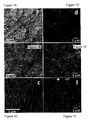
- FIG. 1D A SEM image of a film prepared according to this procedure of the invention is shown in Figs. 1D ,E,F.
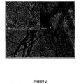
- TEM images are provided in Fig. 2 .
- Procedure 1 above was repeated on a glass substrate for deposition by silanization prior to dipping in the nanowire growth solution.
- Each layer was made of clusters of nanowires with very high aspect ratios.
- a typical cluster contained 10-100 nanowires, each being 2-3 nm wide and the distance between them was of similar dimensions.
- the cluster length was between 10-100 ⁇ m or more, leading to individual nanowire aspect ratios of the order of 50,000.
- the nanowires consisted of mostly gold and silver and were coated with the surfactant material (CTAB).
- the clusters were randomly arranged while the nanowires were well oriented within the clusters.
- Table 1 sheet resistance and transmission of films with a different number of layers. Number of layers Rs (k ⁇ sq.) Transmission at 590nm 1 9 ⁇ 1 99 ⁇ 1% 2 1.5 ⁇ 0.2 98 ⁇ 1% 3 0.36 ⁇ 0.07 93 ⁇ 2%
- the electrical properties of the film can be tuned by the number of layers. While a small reduction in the transmission of the film was observed when the number of layers increased to 3, the sheet resistance was dramatically decreased.
- the contact resistance Rc was low: while a single layer exhibited a sheet resistance of many kilo ohms, the contact resistance for the film as a whole was in the range of 500 and 100 ohm/cm 2 . Considering that the wires cover only a fraction of the surface area, the contact resistance was fairly low.
- the total sheet resistance was not linear with the number of layers (or metal quantity).
- the correlation was Rs proportional to 1/X n , where X is the number of layers and n>1.
- Table 2 sheet resistance and contact resistance of films of a different number of layers. Number of layers Rs (k ⁇ sq.) Rc (k ⁇ ) 1 9 ⁇ 1 1 2 1.5 ⁇ 0.2 0.43 3 0.36 ⁇ 0.07 0.32 bath 0.077 ⁇ 0.020 0.32
- the film of the presented invention comprises very small amounts of metal, as demonstrated in Tables 3.
- Table 3 Metal quantity Minimum Maximum Average Units SEM (estimated) 0.002 0.004 0.003 g/m 2 one layer SEM (estimated) 0.014 g/m 2 two layer + protection layer; 100-150 ohms
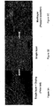
- Figs. 3A provide a SEM image of a film comprising a single nanowire layer prepared according to procedure described in the prior art [13], which involves a post-production drying step.
- Fig. 3B is a SEM image of a film comprising a single nanowire layer with no further treatments
- Fig. 3C is a SEM image of a multilayer nanowires film, according to the present invention.
- the results clearly show a difference in uniformity and quality.
- the prior art procedure which involves a drying step, produces clusters that are thicker but more separated from each other and cover the substrate non-uniformly, as well as non-wire metal aggregates.
- the single monolayer procedure with no further steps produces thinner clusters, more evenly spaced, uniformly covering the substrate, along with relatively low amount of non-wire metal aggregates.
- the multilayer according to procedure 1 also shows clusters, which uniformly covered the substrate, and relatively low amount of non-wire metal aggregates compared to the prior art procedure, and therefore, the film has a homogenous transparency.
- a nanowire film according to the present invention is characterized by a uniform cover of nanowires, leading to a uniform transmittance, as well as good conductivity (low sheet resistance) compared to prior art procedure.
- a short illumination with light from a 100W mercury lamp which provides a strong emission peak at 254 nm over a continuous white spectrum down to about 200 nm was used to photo-reduce metal ions to form small metal seed particles to trigger the start of nanowires growth. About 10 watts hit the 1 cm 2 sample.
- Precursor solution an aqueous solution (10 ml) of cetyltrimethylammonium bromide (CTAB) (0.25M) was mixed with 500 ⁇ l of 25mM tetrachloroauric acid (HAuCl 4 ⁇ 3H 2 O) solution and 250 ⁇ l of 100mM silver nitrate (AgNO 3 ) solution. Then 425 ⁇ l of 1.82M sodium ascorbate solution was added, and the color of the solution changed from a yellow-brown to colorless. The final step involved irradiating the back of a 1 cm 2 fused silica substrate with the mercury lamp for 10 seconds.
- CAB cetyltrimethylammonium bromide
- a second dipping in a gold deposition bath was used to reduce sheet resistance and stabilize the metal nanowires: the aqueous solution (10 ml) of CTAB (0.25M) was mixed with 500 ⁇ l of 25mM HAuCl 4 ⁇ 3H 2 O solution. The substrate with the nanowire film was dipped for 10 minutes in this solution and washed for 1 minute in an ethanol/water 70%/30% solution. Subsequently, metal granulates were obtained on the nanowires.
- seed particles at varying concentrations, were added to the standard nanowire growth solution and carbon coated TEM grid substrates were dipped in the growth solution.
- Nanogold seeds Nanogold seed particles (55-60 gold atoms, ⁇ 1.5 nm) coated with triphenylphsphine - were bought from Molecular Probes.
- CAB cetyltrimethylammonium bromide
- a concentrated seed solution (10-100 ⁇ l - depending on experiment) was added and stirred for a few seconds. Then a few drops were deposited on the TEM substrate for 30 min and maintained at 35°C. Washing was done by dipping the substrate gently into the washing solution of ethanol 70% for 15-30 seconds.
- nanowire clusters were formed.
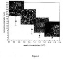
- the seed concentration was reduced to 1.5 ⁇ 10 -10 mol of nanogold seeds per 10 mL growth solution, thicker single nanowires were formed with a thickness of 10 ⁇ 5 nm. Lowering the to 3 ⁇ 10 -11 mol of nanogold seeds per 10 mL growth solution, resulted in nanowires having 15 nm average diameter.
- Undecagold seeds (11 gold atoms, ⁇ 1 nm) coated with triphenylphosphine were bought from Molecular Probes. Procedure 1 was repeated with Undecagold particles at similar concentrations.
- CTAB coated seeds Pre -made seed particles, made by reduction of gold ions in the presence of CTAB.
- Au seeds preparation A CTAB solution (20 mL, 0.05 M) was mixed with 5.0 mL of 0.5 mM HAuCl 4 . To the stirred solution, 0.60 mL of ice-cold 0.010 M NaBH 4 was added, which resulted in the formation of a brownish yellow solution. Vigorous stirring of the seed solution was continued for 2 min. Solution stirring speed was 200 rpm at all stages. After the seed solution was prepared, it was kept at 25°C. Observed seed size ⁇ 2-3 nm.
- nanowires When adding less than 20 ⁇ L seed solution per 10 mL growth solution, thick nanowires resulted (as in the low Nanogold concentration). When the seed solution volumes were larger than 20 ⁇ L seed solution per 10 mL growth solution, nanowire clusters were formed.
- the diameter of the nanowires in the clusters seemed to be fixed (2-3 nm) regardless of seed size or concentration (assuming that both in the commercial small seeds and the pre-made larger seeds there was a substantial amount of seeds smaller than the final nanowire diameter ( ⁇ 2 nm)).
- a wet chemical approach was developed for a unique on-surface synthesis of transparent conductive films consisting of ultrathin gold/silver nanowires directly grown on top of CdSe nanowire array photoconductive devices enclosed in polycarbonate membranes.
- the metal nanowire film formed an ohmic contact to the semiconductor nanowires without additional treatment.
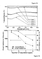
- the sheet resistance and transparency of the metal nanowire arrays could be controlled by the number of metal nanowire layers deposited, ranging from ⁇ 98-99% transmission through the visible range and several kOhm/sq sheet resistance for a single layer, to 80-85% transmission and ⁇ 100 Ohm/sq sheet resistance for 4 layers.
- Fig. 5 shows a schematic presentation of metal nanowire on top of CdSe nanowire array.
- a single film of this type deposited on glass, SiO 2 or transparent plastic would typically have a sheet resistance on the 10 3 ⁇ /sq scale and net light transmission (relative to the bare substrate) of >98% throughout the visible range.
- the seed particles are coated by a surfactant bilayer and when adsorbed with excess surfactant to the solution-substrate interface fuse into larger tubular-vesicular structures. Then, additional metal ions complexed with the CTAB are catalytically reduced within these structures by ascorbate anions available in large excess.
- the high optical transmission in addition to the good contact between layers, permitted to perform multiple layer depositions, where after 3 deposition cycles the sheet resistance decreased to ⁇ 100 ⁇ /sq with an optical transmission of ⁇ 88% at a wavelength of 600 nm.
- Fig. 6A shows a scanning electron microscope (SEM) image of a focused ion beam (FIB) cut of a nanowire film deposited by the self-assembly process, excess solution removed, and the remaining solution film dried without washing.
- SEM scanning electron microscope
- FIB focused ion beam
- Fig. 6D presents an unbinding description of the current understanding of the mechanism leading to nanowire formation; as the substrate is dipped into the growth solution, after triggering the formation of small metal seed particles in solution, the surfactant molecules quickly accumulate at the substrate-solution interface.
- the seed nanoparticles, coated with a surfactant bilayer also adsorb to this interface and apparently induce the formation of elongated vesicular structures which connect between several seed particles to form long nanotubules filled with solution.
- These nanotubules contain the ascorbate ions, which catalytically reduce gold and silver ions complexed with the surfactant at the surface of the seed particles and eventually lead to continuous metal nanowires.
- the ascorbate served as a mild reducing agent.
- Fig. 1 displays the evolution of the resulting nanowire film along the sequential deposition of 3 layers of nanowires, observed both by TEM and SEM.
- the first layer the nanowire network seems to be a random mesh primarily consisting of clusters of 2-3 nm diameter Au-Ag NWs, entwined into 50-100 nm wide clusters together with a small amount of thicker ⁇ 20 nm single nanowires.
- EDS Energy dispersive spectroscopy
- Fig. 7 shows the optical transmission spectra and the corresponding sheet resistance of the Au-Ag NWs random network after 1-4 layers deposition steps.
- a single deposited layer has a net transmission of ⁇ 99% at 600 nm, and a sheet resistance of 5-8 k ⁇ /Sq.
- Deposition of a second layer reduced the sheet resistance to 1-3 k ⁇ /Sq and the resultant transmission to 97-98%.
- Deposition of a third layer further reduced both the sheet resistance and the transmission of the nanowire film to typical values of 100-400 ⁇ /Sq and 88% (at 600 nm), respectively.
- the same process was repeated on various substrates, such as silicon, quartz, and polyethylene terphtalate (PET), with up to 5% variation of the measured optical transparency.
- the transmission data refers to transmission of the film without a substrate.
- TEM and SEM images displayed in Fig. 1 can shed light on the relation between the physical properties of the films and the structural evolution of the films with successive deposition steps.
- the deposition of successive layers resulted in the addition of new nanowire clusters as well as thickening of pre-deposited wires, which caused the suppression of transmission.
- This effect is accompanied by a parallel reduction of the sheet resistivity due to the formation of a denser network possessing an increased number of percolating pathways and is, therefore, characterized by a higher electrical homogeneity. In that manner, control of the trade-off between electrical and optical properties is attained. This fact facilitates the tailoring of the TE properties to the desired application.
- the Au-Ag nanowire film deposited on top of the membrane filled with CdSe NWs was confined to the center of the membrane by a ring of PDMS, protecting the edges from deposition of nanowires that might short-circuit to the bottom gold electrode.
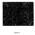
- a representative SEM image of the surface of the resulting device shows a random network of Au-Ag NW clusters covering the membrane surface, enabling electric contact with nearly each CdSe NW and a percolating pathway across the device. Some metallic aggregates adsorbed to the metallic clusters and un-filled pores were observed as well.
- I-V measurements were carried out in a two-probe configuration, employing a probe station, with the bias applied between the Au bottom electrode to the TE via silver paste and the probe station tip.
- Fig. 9 presents the I-V characteristics of the above-mentioned device measured both in dark and under microscope objective white light illumination.
- a device resistance of ca. 3 ⁇ 10 7 ⁇ can be calculated from the dark currents under ⁇ 1V.
- the curve under white-light illumination reveals higher current values throughout the scan from 1V to -1V, implying a decrease of device resistivity by a factor of ca. 15, which was observed in both the positive and negative branches of the I-V curve.
- This invention provides a simple solution-based deposition approach to easily form a metal nanowire-based top transparent contact to a photo-conductive device, showing ohmic current/voltage characteristics.
- the sheet resistance and optical transmission of the film could be controlled by changing the number of deposited nanowire layers.
- an important aspect of the deposition of the TE film is that it does not require any thermal treatment that may harm the underlaying active layer of the device. This is particularly important in devices consisting of organic materials.
- the CdSe nanowires-filled PC membrane is a highly flexible substrate and the conductivity of the metal Au-Ag nanowire top contact did not seem to be affected by membrane curvature. This flexibility is an inherent property of such ultrathin nanowire films.
- the membrane edge was protected by coating it with silicon rubber (GE Bayer Silicones RTV 11/DBT) to avoid a short circuit between the two membrane faces.
- the deposition processes were repeated over carbon coated copper grids, 1 cm 2 Si pieces and 2 cm 2 fused silica pieces for TEM, SEM and optical transmission measurements, respectively.
- Metal nanowire film characterizations The optical transparency of the films was measured against a reference substrate in a fiber-coupled array spectrophotometer (Ocean Optics, S2000) configuration, at a wavelength range of 400-900nm. Sheet resistance measurements were carried out on the same substrates employing a Fluke true rms multi-meter using silver paste at the edges of fused silica substrates for defining the contacts.
- CdSe nanowire array preparation The vertical CdSe NWs array was electrochemically grown, employing a track-etched polycarbonate membrane as a template, as previously described. Briefly, polycarbonate membranes with a specified pore diameter of 100 nm and 6 ⁇ m thickness (Whatman Inc.) were coated with a 200 nm thick thermally-evaporated Au layer. This layer, defining the membrane's back side, served both as a working electrode for the electrochemical deposition process, and as a back contact electrode for the photoconductive device. The membrane was then placed in an electrochemical cell (containing 0.25M CdSO 4 , 0.25M H 2 SO 4 , and 14mM SeO 2 ).
- the deposition was carried out at room temperature employing a CHI621-A potentiostat (CH Instruments, Austin) with a platinum wire as the counter electrode and an Ag/AgCl (3M NaCl) reference electrode. During the electrodeposition process, the potential was held at a constant optimized voltage of 0.75 V (versus the Ag/AgCl reference electrode) for 20 minutes. Once the CdSe NWs were grown, the electrolyte solution was removed and the electrochemical cell was washed with distilled water, the membrane was carefully wiped and washed with water to remove CdSe residue grown on its surface and then dried under a dry N 2 stream.
- Photoactive device characterizations were carried out in a two-probe configuration, employing a probe station (Janis, ST-500), with the bias applied between the Au bottom electrode to the TE via silver paste and the probe station tip.
- the voltage reading was converted to current using a preamplifier (DL 1211) and was collected through a computer-controlled rack-mounted breakout accessory (National Instruments, BNC 2090) and a DAQ card (National Instruments, PCI-MIO-16XE).
- ITO Indium Tin Oxide
- MNWM metal nanowire mesh
- AuAg nanowire mesh (AuAgNWM) electrode was prepared.
- the substrate of choice for this process was fused silica and the penetration depth of the light in the solution was estimated to be 14 ⁇ m according to absorbance measurement of the precursor solution before exposure to light radiation (supporting information). This allows for an AuAgNWM to be formed in close proximity to the substrate/solution interface.
- the AuAgNWM film obtained by the uv-radiation method had transmittance (at 590nm) and sheet resistance values of 97.46 ⁇ 0.96(%) and 3.0 ⁇ 1.4(kohm), respectively (see Fig. 10 ).
- the initial sheet resistance was unstable and increases as time passed. The exact reason for conduction degradation is still not completely understood, but it is reasonable to assume that stability of nanowires requires proper surfactant capping which could be removed or damaged due to exposure to the humidity in air.
- gold was additionally precipitated on the nanowires by dipping the substrate for 10 minutes in a treatment solution containing the same concentration of CTAB and gold ions as the precursor solution.
- Fig. 11 Shown in Fig. 11 is a SEM image of a AuAgNWM film after the treatment. Films created by this method were used as bottom electrodes for OLED devices.
- Fig. 12 presents a schematic illustration of an OLED device based on an AuAgNWM electrode.
- the device can be easily fabricated and does not require any buffer (passivation) layers such PEDOT:PSS or LiF which are usually incorporated in OLED devices for adjusting the components' work functions.
- buffer (passivation) layers such PEDOT:PSS or LiF which are usually incorporated in OLED devices for adjusting the components' work functions.
- the work functions of ITO and AuAgNWM electrode, -4.7eV and -5.1eV respectively are quite suitable for the organic layer of MEH-PPV used in the device, which has a HOMO of -5.02eV.
- the work function of aluminum is -4.3eV and therefore not as suitable for MEH-PPV's LUMO of -2.7eV, however the incorporation of other top electrodes such as those based on calcium adds complexity and cost to the device and thus were dismissed.
- the I-V curves for both types of devices show typical OLED behavior and luminance characterizations have comparable efficiency proving that AuAgNWM electrodes are capable of functioning as alternatives to transparent conducting oxides (see Fig. 13 ). It is clearly seen that V turn-on of our electrode is higher and provides half the amount of light the ITO based OLEDs produce. The reasons for this are twofold; first, the conductivity of the AuAgNWM electrode is about a quarter of the conductivity of ITO. Secondly, the porous morphology of AuAgNWM electrode (see Fig. 11 ) means that there is a smaller effective area in comparison to the continuous ITO electrode.
- the ITO based OLED provides only double the amount of light generated by the AuAgNWM based OLED.
- the AuAgNWM electrode can be planarized with a buffer layer, such as a layer of PEDOT:PSS, in order to achieve uniform morphology, higher conductivity and improve hole-injection through the anode.
- the spectrum of light emitted from the OLED device is similar to other MEH-PPV devices described in the literature.
- Precursor solution the aqueous solution (10 ml) of cetyltrimethylammonium bromide (CTAB) (0.25M) was mixed with 500 ⁇ l of 25mM tetrachloroauric acid (HAuCl 4 ⁇ 3H 2 O) solution and 250 ⁇ l of 100mM silver nitrate (AgNO 3 ) solution. Then 425 ⁇ l of 1.82M sodium ascorbate solution was added, and the color of the solution changed from a yellow-brown to a colorless one. The final step involved radiating the solution with a mercury lamp for 10 seconds. The light passes through the fused silica substrate, which was located at the liquid-air interface producing a solid (substrate)-liquid interface.
- CAB cetyltrimethylammonium bromide
- the substrate was pulled out and the remaining thin film of the precursor solution was allowed to dry out for a few seconds. Then, the substrate was washed for 1 minute in an ethanol/water 70%/30% solution. Two strips of silver paint were applied on parallel edges of the substrate in order to create two electrodes for the measurement of sheet resistance.
- Treatment solution the aqueous solution (10 ml) of CTAB (0.25M) was mixed with 500 ⁇ l of 25mM HAuCl 4 ⁇ 3H 2 O solution.
- the AuAgNWM substrates were subsequently dipped for 10 minutes in the treatment solution and washed for 1 minute in an ethanol/water 70%/30% solution.
- OLEDs were fabricated with AuAgNWM electrodes as well as on commercial ITO electrodes.
- the two types of transparent electrodes were used as a bottom electrode on which a solution of MEH-PPV in chloroform (3 mg/ml) was spin coated at 1500 rpm for 40 seconds.
- Top contacts were evaporated over the MEH-PPV layer by consecutive deposition of aluminum and gold, using a shadow mask (see Fig. 12 ).
- the devices were examined with an electroluminescence measurement system. For each device the I-V and luminance curves were produced and in addition the electroluminescence spectrums were measured at maximum light output.
- the same type of devices can also be fabricated using the standard nanowire deposition technique with borohydride reduction trigger or addition of pre-prepared small metal seed particles (typically ⁇ 2 nm in size). There is no basic difference in the films prepared by UV irradiation and this type.
Landscapes
- Chemical & Material Sciences (AREA)
- Metallurgy (AREA)
- Chemical Kinetics & Catalysis (AREA)
- Engineering & Computer Science (AREA)
- Materials Engineering (AREA)
- Mechanical Engineering (AREA)
- General Chemical & Material Sciences (AREA)
- Organic Chemistry (AREA)
- Dispersion Chemistry (AREA)
- Non-Insulated Conductors (AREA)
- Manufacture Of Metal Powder And Suspensions Thereof (AREA)
- Laminated Bodies (AREA)
- Powder Metallurgy (AREA)
- Manufacturing Of Electric Cables (AREA)
Claims (14)
- Ein leitender Film umfassend mindestens eine leitende Schicht, umfassend eine Anordnung von elektrisch leitenden Metall-Nanodrähten, wobei die Nanodrähte ein durchschnittliches Aspektverhältnis von mindestens 100,000 haben, wobei 70% oder 80% oder 90% oder 95% oder 99% der genannten Nanodrähte in einem oder mehreren Clustern angeordnet sind, worin jeder Cluster zwei oder mehr Nanodrähte parallel zueinander entlang derselben Achse ausgerichtet umfasst, worin der Drahtabstand innerhalb des Clusters weniger als 20 nm beträgt.
- Der Film gemäß Anspruch 1, umfassend mindestens einen Schutzfilm.
- Der Film gemäß Anspruch 1, worin die genannten Nanodrähte in einem Film aus mindestens einem oberflächenaktiven Stoff beschichtet werden.
- Der Film gemäß Anspruch 3, worin die Nanodrähte in den genannten Clustern in die gleiche Richtung ausgerichtet sind.
- Der Film gemäß Anspruch 4, worin die Nanodrähte verzweigt und/oder gebogen sind.
- Der Film gemäß Anspruch 3, worin die Nanodrähte in einer organischen Matrize angeordnet sind, die durch ein umgebendes oberflächenaktives Material gebildet wird.
- Der Film gemäß Anspruch 1, worin der genannte Cluster homogen voneinander beabstandete Nanodrähte umfasst.
- Ein Verfahren für die Herstellung eines leitenden Films gemäß Anspruch 1, wobei das Verfahren Folgendes umfasst:(a) Herstellen einer wässerigen Vorläuferlösung umfassend mindestens einen Metallvorläufer, mindestens einen oberflächenaktiven Stoff und mindestens ein Metall-reduzierendes Mittel;(b) Bilden eines dünnen Films aus der Vorläuferlösung auf mindestens einem Teil einer Oberfläche des Substrats; und(c) Erlauben, dass sich eine Schicht von Metall-Nanodrähten bildet;(d) Wahlweise Wiederholen der Schritte (a), (b) und (c) auf der Schicht von Metall-Nanodrähten (erhalten in Schritt (c)), worin die genannten Schritte ein oder mehrmals wiederholt werden, um dabei eine Aufeinanderstapelung von zwei oder mehreren Metall-Nanodrahtschichten zu erhalten; und(e) Wahlweise behandeln des Films mit einer Lösung, die mindestens einen oberflächenaktiven Stoff, mindestens einen Metallvorläufer und mindestens ein schwaches Metall-reduzierendes Mittel umfasst;worin einer oder beide der Schritte (d) und (e) durchgeführt werden; um dadurch einen leitenden Film von Nanodrähten auf mindestens einem Teil der genannten Oberfläche zu erhalten.
- Das Verfahren gemäß Anspruch 8, worin die genannte Vorläuferlösung Metall-, Halbleiter- oder Metalloxidnanopartikel umfasst.
- Das Verfahren gemäß Anspruch 8, das Folgendes umfasst:(a) Herstellen einer wässerigen Vorläuferlösung umfassend mindestens einen Metallvorläufer, mindestens einen oberflächenaktiven Stoff und mindestens ein Metall-reduzierendes Mittel, worin das genannte mindestens eine Metall-reduzierende Mittel die Bildung von Metallimpfpartikeln in Lösung triggert;(b) Bilden eines dünnen Films aus der Vorläuferlösung auf mindestens einem Teil einer Oberfläche des Substrats; und(c) Erlauben, dass sich eine Schicht von Metall-Nanodrähten bildet;(d) Behandeln des Films mit einer Lösung umfassend mindestens einen oberflächenaktiven Stoff, mindestens einen Metallvorläufer und mindestens ein schwaches Metall-reduzierendes Mittel;wodurch ein leitender Film von Nanodrähten auf mindestens einem Teil der genannten Oberfläche erhalten wird.
- Das Verfahren gemäß Anspruch 8, das Folgendes umfasst:(a) Herstellen einer wässerigen Vorläuferlösung, wobei die genannte Lösung folgendermaßen hergestellt wird:(i) Bilden einer Lösung aus mindestens einem oberflächenaktiven Stoff bei einer Konzentration von zwischen 1-10% (Massenprozent), mindestens einem Goldmetallvorläufer und Natriumascorbat in einem wässerigen Medium;(ii) Hinzufügen von mindestens einem Silbermetallvorläufer;(b) Bilden einer Schicht aus der Lösung von Schritt (a) auf mindestens einem Teil einer Oberfläche eines Substrats; und(c) Wahlweise Wiederholen von Schritt (b) ein oder mehrere Male auf einer vorhergehenden Schicht, wie weiter oben ausführlich dargelegt;(d) Behandeln des Films mit einer Lösung, die mindestens einen oberflächenaktiven Stoff, mindestens einen Metallvorläufer und mindestens ein schwaches Metall-reduzierendes Mittel umfasst;wodurch ein Gold/Silber-Nanodrahtfilm auf mindestens einem Teil einer Oberfläche erhalten wird.
- Das Verfahren gemäß Anspruch 8, das folgendes umfasst:(a) Herstellen einer wässerigen Vorläuferlösung, wobei die genannte Lösung folgendermaßen hergestellt wird:(i) Bilden einer Lösung aus mindestens einem oberlfächenaktiven Stoff bei einer Konzentration zwischen 1-10% (Massenprozent), mindestens einem Gold-Metallvorläufer und mindestens einem SilberMetallvorläufer und mindestens einem Ascorbat-Reduktionsmittel in einem wässerigen Medium;(ii) Hinzufügen eines Metallborhydrids, und/oder Nanopartikeln gewählt aus Metall-Nanopartikeln, Halbleiter-Nanopartikeln und Metalloxid-Nanopartikeln;(b) Bilden einer Schicht aus der Lösung von Schritt (a) auf mindestens einem Teil einer Oberfläche eines Substrats; und(c) Wahlweise Wiederholen von Schritt (b) ein oder mehrere Male auf einer vorhergehenden Schicht;(d) Behandeln des Films mit einer Lösung, die mindestens einen oberflächenaktiven Stoff, mindestens einen Metallvorläufer und mindestens ein schwaches Metall-reduzierendes Mittel umfasst;wodurch ein Gold/Silber-Nanodrahtfilm auf mindestens einem Teil der genannten Oberfläche erhalten wird.
- Eine Elektrodenstruktur umfassend einen leitenden Film gemäß Anspruch 1, oder hergestellt durch das Verfahren von Anspruch 8.
- Eine Vorrichtung integriert mit einem Film gemäß Anspruch 1, oder hergestellt durch das Verfahren von Anspruch 8, wobei die Vorrichtung gewählt ist aus Photoleitern, Photodioden; Solarzellen; Leuchtdioden (LEDs), organischen Leuchtdioden, Lasern; Lichtsensoren, spezialisierten Transistoren, organischen Transistoren, anorganischen Transistoren, und Hybrid-Transistoren.
Applications Claiming Priority (2)
| Application Number | Priority Date | Filing Date | Title |
|---|---|---|---|
| US201261605421P | 2012-03-01 | 2012-03-01 | |
| PCT/IL2013/050184 WO2013128458A1 (en) | 2012-03-01 | 2013-02-28 | Conductive nanowire films |
Publications (3)
| Publication Number | Publication Date |
|---|---|
| EP2820657A1 EP2820657A1 (de) | 2015-01-07 |
| EP2820657A4 EP2820657A4 (de) | 2015-12-02 |
| EP2820657B1 true EP2820657B1 (de) | 2019-11-27 |
Family
ID=49081743
Family Applications (1)
| Application Number | Title | Priority Date | Filing Date |
|---|---|---|---|
| EP13754789.9A Active EP2820657B1 (de) | 2012-03-01 | 2013-02-28 | Leitende nanodrahtfilme |
Country Status (4)
| Country | Link |
|---|---|
| US (2) | US9373515B2 (de) |
| EP (1) | EP2820657B1 (de) |
| CN (1) | CN104508758B (de) |
| WO (1) | WO2013128458A1 (de) |
Families Citing this family (59)
| Publication number | Priority date | Publication date | Assignee | Title |
|---|---|---|---|---|
| US9574272B2 (en) | 2008-09-02 | 2017-02-21 | Ramot At Tel-Aviv University Ltd | Metal nanowire thin-films |
| CN104508758B (zh) | 2012-03-01 | 2018-08-07 | 雷蒙特亚特特拉维夫大学有限公司 | 导电纳米线膜 |
| US9920207B2 (en) | 2012-06-22 | 2018-03-20 | C3Nano Inc. | Metal nanostructured networks and transparent conductive material |
| US10029916B2 (en) | 2012-06-22 | 2018-07-24 | C3Nano Inc. | Metal nanowire networks and transparent conductive material |
| EP2958481A4 (de) | 2013-02-20 | 2017-03-08 | Sloan-Kettering Institute for Cancer Research | Ramanbildgebungsvorrichtung mit weitem sichtfeld und zugehörige verfahren |
| US10020807B2 (en) | 2013-02-26 | 2018-07-10 | C3Nano Inc. | Fused metal nanostructured networks, fusing solutions with reducing agents and methods for forming metal networks |
| US10173265B2 (en) * | 2013-03-22 | 2019-01-08 | University of Pittsburgh—of the Commonwealth System of Higher Education | Method for producing small metal alloy nanoparticles |
| KR20150001528A (ko) * | 2013-06-27 | 2015-01-06 | 삼성전자주식회사 | 수직형 유기 발광 트랜지스터 및 이를 구비한 유기 엘이디 조명장치 |
| US11274223B2 (en) | 2013-11-22 | 2022-03-15 | C3 Nano, Inc. | Transparent conductive coatings based on metal nanowires and polymer binders, solution processing thereof, and patterning approaches |
| KR102142334B1 (ko) * | 2013-12-27 | 2020-08-07 | 주식회사 동진쎄미켐 | 탄소-메탈 복합체의 제조방법 |
| US10081058B2 (en) * | 2014-04-11 | 2018-09-25 | Cam Holding Corporation | Methods of controlling nanowire morphology |
| US9183968B1 (en) | 2014-07-31 | 2015-11-10 | C3Nano Inc. | Metal nanowire inks for the formation of transparent conductive films with fused networks |
| KR102238180B1 (ko) * | 2014-08-05 | 2021-04-08 | 엘지디스플레이 주식회사 | 플렉서블 표시장치 및 그 제조방법 |
| US9808781B2 (en) * | 2014-08-08 | 2017-11-07 | The University Of Hong Kong | Conductive metal networks including metal nanowires and metal nanoparticles and methods of fabricating the same |
| TWI561462B (en) * | 2014-10-07 | 2016-12-11 | Iner Aec Executive Yuan | A method for forming dendritic silver with periodic structure as light-trapping layer |
| GB201500748D0 (en) * | 2015-01-16 | 2015-03-04 | Cambridge Display Tech Ltd | Method of forming a light-emitting device |
| WO2016122004A1 (en) * | 2015-01-26 | 2016-08-04 | Duksan Hi-Metal Co., Ltd. | Metal nanowire, method for synthesizing the metal nanowire, and transparent electrode and organic light emitting diode including the metal nanowire manufactured by the method |
| US9468989B2 (en) | 2015-02-26 | 2016-10-18 | Northrop Grumman Systems Corporation | High-conductivity bonding of metal nanowire arrays |
| US20160374209A1 (en) * | 2015-06-18 | 2016-12-22 | Postech Academy - Industry Foundation | Method of fabricating metal nanowire pattern |
| WO2017004301A1 (en) * | 2015-07-01 | 2017-01-05 | Memorial Sloan Kettering Cancer Center | Anisotropic particles, methods and uses thereof |
| US10829605B2 (en) | 2015-07-02 | 2020-11-10 | Sabic Global Technologies B.V. | Process and material for growth of adsorbed compound via nanoscale-controlled resistive heating and uses thereof |
| KR20170018718A (ko) * | 2015-08-10 | 2017-02-20 | 삼성전자주식회사 | 비정질 합금을 이용한 투명 전극 및 그 제조 방법 |
| WO2017033444A1 (en) * | 2015-08-24 | 2017-03-02 | Okinawa Institute Of Science And Technology School Corporation | In-situ growth and catalytic nanoparticle decoration of metal oxide nanowires |
| DE102015115004A1 (de) * | 2015-09-07 | 2017-03-09 | Leibniz-Institut Für Neue Materialien Gemeinnützige Gmbh | Verfahren zur Herstellung von strukturierten Oberflächen |
| ES2625024B1 (es) * | 2015-12-18 | 2018-05-10 | Consejo Superior De Investigaciones Cientificas | Material que comprende tectómeros de oligoglicina y nanohilos |
| CN105568270B (zh) * | 2016-01-11 | 2018-07-10 | 合肥银派科技有限公司 | 一种银纳米线焊接液及焊接成膜方法 |
| ES2638068B1 (es) * | 2016-02-29 | 2018-09-06 | Universidad De La Laguna | Célula fotoeléctrica de alta eficiencia |
| EP3440904A4 (de) * | 2016-04-07 | 2019-12-11 | Technology Innovation Momentum Fund (Israel) Limited Partnership | Drucken von nanodrahtfolien |
| CN105798447B (zh) * | 2016-04-12 | 2018-06-29 | 苏州大学 | 一种利用纳米互连制备金属纳米线的方法及其应用 |
| JP6139009B1 (ja) * | 2016-12-12 | 2017-05-31 | マイクロ波化学株式会社 | 銀ナノワイヤの製造方法、銀ナノワイヤ、分散液、及び透明導電膜 |
| US11387012B2 (en) * | 2017-05-01 | 2022-07-12 | Monash University | Standing nanowire-based elastic conductor |
| KR102081391B1 (ko) * | 2017-09-22 | 2020-02-25 | 한양대학교 에리카산학협력단 | 이방성 이중금속 나노와이어, 이중금속 나노와이어 내장 폴리머 나노섬유, 이중금속 나노와이어 포함 sers 기판, 이의 제조방법 및 용도 |
| US10860618B2 (en) | 2017-09-25 | 2020-12-08 | Splunk Inc. | Low-latency streaming analytics |
| CN107741418B (zh) * | 2017-10-19 | 2020-05-22 | 重庆大学 | 基于针尖增强拉曼技术检测金属封装内部分子信号的方法 |
| US10997180B2 (en) | 2018-01-31 | 2021-05-04 | Splunk Inc. | Dynamic query processor for streaming and batch queries |
| CN109239990A (zh) * | 2018-08-22 | 2019-01-18 | 苏州美嘉写智能显示科技有限公司 | 一种上转化纳米材料掺杂的液晶复合薄膜及其制备方法 |
| US11106107B2 (en) * | 2018-09-09 | 2021-08-31 | Zhejiang Jingyi New Material Technology Co., Ltd | Ultra-flexible and robust silver nanowire films for controlling light transmission and method of making the same |
| US10936585B1 (en) | 2018-10-31 | 2021-03-02 | Splunk Inc. | Unified data processing across streaming and indexed data sets |
| CN110102264B (zh) * | 2019-06-04 | 2021-03-02 | 太原理工大学 | 一种超高磁响应性纳米团簇微球的制备及废水处理方法 |
| CN112151204A (zh) * | 2019-06-26 | 2020-12-29 | 南京大学昆山创新研究院 | 一种背电极浆料和其制备方法及对应背电极制备方法 |
| US11238048B1 (en) | 2019-07-16 | 2022-02-01 | Splunk Inc. | Guided creation interface for streaming data processing pipelines |
| US20220272798A1 (en) * | 2019-07-31 | 2022-08-25 | Ited Inc. | Transparent heating film |
| CN110560703B (zh) * | 2019-09-18 | 2020-09-18 | 清华大学 | 基于飞秒激光的高催化活性金纳米棒制备方法及其系统 |
| CN110681873A (zh) * | 2019-10-16 | 2020-01-14 | 重庆邮电大学 | 一种基于铁纳米线的柔性应变传感器及其制备方法 |
| CN110739097B (zh) * | 2019-11-07 | 2021-07-16 | 浙江大学 | 功函数可调的银纳米线复合透明导电薄膜的制备方法 |
| US11614923B2 (en) | 2020-04-30 | 2023-03-28 | Splunk Inc. | Dual textual/graphical programming interfaces for streaming data processing pipelines |
| US11987717B2 (en) * | 2020-07-10 | 2024-05-21 | The Research Foundation For The State University Of New York | Air-stable conductive ink |
| US11650995B2 (en) | 2021-01-29 | 2023-05-16 | Splunk Inc. | User defined data stream for routing data to a data destination based on a data route |
| US12164524B2 (en) | 2021-01-29 | 2024-12-10 | Splunk Inc. | User interface for customizing data streams and processing pipelines |
| US11687487B1 (en) | 2021-03-11 | 2023-06-27 | Splunk Inc. | Text files updates to an active processing pipeline |
| CN113130136B (zh) * | 2021-04-19 | 2023-11-14 | 重庆烯宇新材料科技有限公司 | 纳米银线mxene复合透明导电膜、制备方法及应用 |
| US11663219B1 (en) | 2021-04-23 | 2023-05-30 | Splunk Inc. | Determining a set of parameter values for a processing pipeline |
| US11604789B1 (en) | 2021-04-30 | 2023-03-14 | Splunk Inc. | Bi-directional query updates in a user interface |
| US12242892B1 (en) | 2021-04-30 | 2025-03-04 | Splunk Inc. | Implementation of a data processing pipeline using assignable resources and pre-configured resources |
| US11989592B1 (en) | 2021-07-30 | 2024-05-21 | Splunk Inc. | Workload coordinator for providing state credentials to processing tasks of a data processing pipeline |
| US12164522B1 (en) | 2021-09-15 | 2024-12-10 | Splunk Inc. | Metric processing for streaming machine learning applications |
| CN114927618B (zh) * | 2022-03-18 | 2025-12-16 | 江苏大学 | 一种基于Bayer模型的多波段复合光电探测器及其制备方法 |
| CN116539546B (zh) * | 2023-06-28 | 2023-09-15 | 江西省农业科学院农产品质量安全与标准研究所 | 一种四价硒离子表面等离子体共振检测方法及应用 |
| CN120518328B (zh) * | 2025-07-22 | 2026-03-06 | 电子科技大学 | 微纳小球自组装掩膜制备随机网栅透明导电薄膜的方法 |
Family Cites Families (15)
| Publication number | Priority date | Publication date | Assignee | Title |
|---|---|---|---|---|
| US5294370A (en) | 1988-11-15 | 1994-03-15 | Hbt Holland Biotechnology B.V. | Selenium or tellurium elemental hydrosols and their preparation |
| JP2004064039A (ja) | 2002-06-07 | 2004-02-26 | Fuji Photo Film Co Ltd | パターン形成方法及びパターン形成装置 |
| US7051945B2 (en) * | 2002-09-30 | 2006-05-30 | Nanosys, Inc | Applications of nano-enabled large area macroelectronic substrates incorporating nanowires and nanowire composites |
| JP4636454B2 (ja) | 2003-05-13 | 2011-02-23 | 三菱マテリアル株式会社 | 金属ナノロッドの製造方法と用途 |
| US20060267595A1 (en) * | 2005-03-11 | 2006-11-30 | Wavelength Electronics, Inc. | Electrical component with fractional order impedance |
| ATE532217T1 (de) | 2005-08-12 | 2011-11-15 | Cambrios Technologies Corp | Verfahren zur herstellung von transparente leiter auf nanodrahtbasis |
| US7736910B2 (en) | 2005-10-04 | 2010-06-15 | Calypte Biomedical Corporation | One-step production of gold sols |
| TWI426531B (zh) * | 2006-10-12 | 2014-02-11 | 坎畢歐科技公司 | 以奈米線為主之透明導體及其應用 |
| KR100790216B1 (ko) | 2006-10-17 | 2008-01-02 | 삼성전자주식회사 | 전도성 분산제를 이용한 cnt 투명전극 및 그의 제조방법 |
| WO2009063744A1 (ja) * | 2007-11-16 | 2009-05-22 | Konica Minolta Holdings, Inc. | 金属ナノワイヤの製造方法、金属ナノワイヤ及び透明導電体 |
| US9574272B2 (en) * | 2008-09-02 | 2017-02-21 | Ramot At Tel-Aviv University Ltd | Metal nanowire thin-films |
| GB0908300D0 (en) * | 2009-05-14 | 2009-06-24 | Dupont Teijin Films Us Ltd | Polyester films |
| US8455048B1 (en) * | 2010-03-18 | 2013-06-04 | Sandia Corporation | Method for making nanomaterials |
| TWI549900B (zh) | 2010-03-23 | 2016-09-21 | 坎畢歐科技公司 | 奈米結構透明導體之圖案化蝕刻 |
| CN104508758B (zh) | 2012-03-01 | 2018-08-07 | 雷蒙特亚特特拉维夫大学有限公司 | 导电纳米线膜 |
-
2013
- 2013-02-28 CN CN201380015984.4A patent/CN104508758B/zh not_active Expired - Fee Related
- 2013-02-28 EP EP13754789.9A patent/EP2820657B1/de active Active
- 2013-02-28 US US14/382,396 patent/US9373515B2/en not_active Expired - Fee Related
- 2013-02-28 WO PCT/IL2013/050184 patent/WO2013128458A1/en not_active Ceased
-
2016
- 2016-05-23 US US15/161,969 patent/US10403414B2/en not_active Expired - Fee Related
Non-Patent Citations (1)
| Title |
|---|
| None * |
Also Published As
| Publication number | Publication date |
|---|---|
| EP2820657A1 (de) | 2015-01-07 |
| WO2013128458A1 (en) | 2013-09-06 |
| CN104508758B (zh) | 2018-08-07 |
| US9373515B2 (en) | 2016-06-21 |
| EP2820657A4 (de) | 2015-12-02 |
| US10403414B2 (en) | 2019-09-03 |
| US20160268013A1 (en) | 2016-09-15 |
| US20150104936A1 (en) | 2015-04-16 |
| CN104508758A (zh) | 2015-04-08 |
Similar Documents
| Publication | Publication Date | Title |
|---|---|---|
| EP2820657B1 (de) | Leitende nanodrahtfilme | |
| US10237974B2 (en) | Metal nanowire thin-films | |
| US12407349B2 (en) | Fused metal nanostructured networks, fusing solutions with reducing agents and methods for forming metal networks | |
| TWI576866B (zh) | 以奈米線爲主之透明導體及其應用 | |
| Kang et al. | Polymer-metal hybrid transparent electrodes for flexible electronics | |
| JP5472889B2 (ja) | 金属ナノワイヤ、及び金属ナノワイヤを含む透明導電体 | |
| TW201200467A (en) | Nanowire-based transparent conductors and methods of patterning same | |
| KR20180004130A (ko) | 귀금속이 코팅된 실버 나노와이어, 이 코팅의 제조방법 및 안정화된 투명 전도성 필름 | |
| Dinh et al. | Silver nanowires: a promising transparent conducting electrode material for optoelectronic and electronic applications | |
| Peng et al. | Colossal figure of merit in transparent-conducting metallic ribbon networks | |
| Wang et al. | Programmed ultrafast scan welding of Cu nanowire networks with a pulsed ultraviolet laser beam for transparent conductive electrodes and flexible circuits | |
| Zhang et al. | Solution process formation of high performance, stable nanostructured transparent metal electrodes via displacement-diffusion-etch process | |
| US11240917B2 (en) | Printing of nanowire films | |
| Deignan | Corrosion study of silver nanowires | |
| Stewart | The Impact of Morphology and Composition on the Resistivity and Oxidation Resistance of Metal Nanostructure Films | |
| HK1177327B (en) | Nanowire-based transparent conductors and methods of patterning same |
Legal Events
| Date | Code | Title | Description |
|---|---|---|---|
| PUAI | Public reference made under article 153(3) epc to a published international application that has entered the european phase |
Free format text: ORIGINAL CODE: 0009012 |
|
| 17P | Request for examination filed |
Effective date: 20140930 |
|
| AK | Designated contracting states |
Kind code of ref document: A1 Designated state(s): AL AT BE BG CH CY CZ DE DK EE ES FI FR GB GR HR HU IE IS IT LI LT LU LV MC MK MT NL NO PL PT RO RS SE SI SK SM TR |
|
| AX | Request for extension of the european patent |
Extension state: BA ME |
|
| DAX | Request for extension of the european patent (deleted) | ||
| RA4 | Supplementary search report drawn up and despatched (corrected) |
Effective date: 20151102 |
|
| RIC1 | Information provided on ipc code assigned before grant |
Ipc: G02F 1/1343 20060101ALI20151027BHEP Ipc: C01G 7/00 20060101ALI20151027BHEP Ipc: H01B 5/14 20060101ALI20151027BHEP Ipc: B82Y 40/00 20110101ALI20151027BHEP Ipc: H01L 31/0224 20060101ALI20151027BHEP Ipc: H01B 1/22 20060101AFI20151027BHEP Ipc: C01G 5/00 20060101ALI20151027BHEP Ipc: B05D 5/12 20060101ALI20151027BHEP Ipc: C23C 18/44 20060101ALI20151027BHEP Ipc: B32B 15/02 20060101ALI20151027BHEP |
|
| STAA | Information on the status of an ep patent application or granted ep patent |
Free format text: STATUS: EXAMINATION IS IN PROGRESS |
|
| 17Q | First examination report despatched |
Effective date: 20180611 |
|
| GRAP | Despatch of communication of intention to grant a patent |
Free format text: ORIGINAL CODE: EPIDOSNIGR1 |
|
| STAA | Information on the status of an ep patent application or granted ep patent |
Free format text: STATUS: GRANT OF PATENT IS INTENDED |
|
| INTG | Intention to grant announced |
Effective date: 20190624 |
|
| GRAS | Grant fee paid |
Free format text: ORIGINAL CODE: EPIDOSNIGR3 |
|
| GRAA | (expected) grant |
Free format text: ORIGINAL CODE: 0009210 |
|
| STAA | Information on the status of an ep patent application or granted ep patent |
Free format text: STATUS: THE PATENT HAS BEEN GRANTED |
|
| AK | Designated contracting states |
Kind code of ref document: B1 Designated state(s): AL AT BE BG CH CY CZ DE DK EE ES FI FR GB GR HR HU IE IS IT LI LT LU LV MC MK MT NL NO PL PT RO RS SE SI SK SM TR |
|
| REG | Reference to a national code |
Ref country code: GB Ref legal event code: FG4D |
|
| REG | Reference to a national code |
Ref country code: CH Ref legal event code: EP |
|
| REG | Reference to a national code |
Ref country code: AT Ref legal event code: REF Ref document number: 1207615 Country of ref document: AT Kind code of ref document: T Effective date: 20191215 |
|
| REG | Reference to a national code |
Ref country code: DE Ref legal event code: R096 Ref document number: 602013063370 Country of ref document: DE |
|
| REG | Reference to a national code |
Ref country code: IE Ref legal event code: FG4D |
|
| REG | Reference to a national code |
Ref country code: NL Ref legal event code: MP Effective date: 20191127 |
|
| REG | Reference to a national code |
Ref country code: LT Ref legal event code: MG4D |
|
| PG25 | Lapsed in a contracting state [announced via postgrant information from national office to epo] |
Ref country code: NO Free format text: LAPSE BECAUSE OF FAILURE TO SUBMIT A TRANSLATION OF THE DESCRIPTION OR TO PAY THE FEE WITHIN THE PRESCRIBED TIME-LIMIT Effective date: 20200227 Ref country code: FI Free format text: LAPSE BECAUSE OF FAILURE TO SUBMIT A TRANSLATION OF THE DESCRIPTION OR TO PAY THE FEE WITHIN THE PRESCRIBED TIME-LIMIT Effective date: 20191127 Ref country code: BG Free format text: LAPSE BECAUSE OF FAILURE TO SUBMIT A TRANSLATION OF THE DESCRIPTION OR TO PAY THE FEE WITHIN THE PRESCRIBED TIME-LIMIT Effective date: 20200227 Ref country code: LV Free format text: LAPSE BECAUSE OF FAILURE TO SUBMIT A TRANSLATION OF THE DESCRIPTION OR TO PAY THE FEE WITHIN THE PRESCRIBED TIME-LIMIT Effective date: 20191127 Ref country code: SE Free format text: LAPSE BECAUSE OF FAILURE TO SUBMIT A TRANSLATION OF THE DESCRIPTION OR TO PAY THE FEE WITHIN THE PRESCRIBED TIME-LIMIT Effective date: 20191127 Ref country code: GR Free format text: LAPSE BECAUSE OF FAILURE TO SUBMIT A TRANSLATION OF THE DESCRIPTION OR TO PAY THE FEE WITHIN THE PRESCRIBED TIME-LIMIT Effective date: 20200228 Ref country code: NL Free format text: LAPSE BECAUSE OF FAILURE TO SUBMIT A TRANSLATION OF THE DESCRIPTION OR TO PAY THE FEE WITHIN THE PRESCRIBED TIME-LIMIT Effective date: 20191127 Ref country code: ES Free format text: LAPSE BECAUSE OF FAILURE TO SUBMIT A TRANSLATION OF THE DESCRIPTION OR TO PAY THE FEE WITHIN THE PRESCRIBED TIME-LIMIT Effective date: 20191127 Ref country code: LT Free format text: LAPSE BECAUSE OF FAILURE TO SUBMIT A TRANSLATION OF THE DESCRIPTION OR TO PAY THE FEE WITHIN THE PRESCRIBED TIME-LIMIT Effective date: 20191127 |
|
| PG25 | Lapsed in a contracting state [announced via postgrant information from national office to epo] |
Ref country code: IS Free format text: LAPSE BECAUSE OF FAILURE TO SUBMIT A TRANSLATION OF THE DESCRIPTION OR TO PAY THE FEE WITHIN THE PRESCRIBED TIME-LIMIT Effective date: 20200327 Ref country code: HR Free format text: LAPSE BECAUSE OF FAILURE TO SUBMIT A TRANSLATION OF THE DESCRIPTION OR TO PAY THE FEE WITHIN THE PRESCRIBED TIME-LIMIT Effective date: 20191127 Ref country code: RS Free format text: LAPSE BECAUSE OF FAILURE TO SUBMIT A TRANSLATION OF THE DESCRIPTION OR TO PAY THE FEE WITHIN THE PRESCRIBED TIME-LIMIT Effective date: 20191127 |
|
| PG25 | Lapsed in a contracting state [announced via postgrant information from national office to epo] |
Ref country code: AL Free format text: LAPSE BECAUSE OF FAILURE TO SUBMIT A TRANSLATION OF THE DESCRIPTION OR TO PAY THE FEE WITHIN THE PRESCRIBED TIME-LIMIT Effective date: 20191127 |
|
| PG25 | Lapsed in a contracting state [announced via postgrant information from national office to epo] |
Ref country code: DK Free format text: LAPSE BECAUSE OF FAILURE TO SUBMIT A TRANSLATION OF THE DESCRIPTION OR TO PAY THE FEE WITHIN THE PRESCRIBED TIME-LIMIT Effective date: 20191127 Ref country code: EE Free format text: LAPSE BECAUSE OF FAILURE TO SUBMIT A TRANSLATION OF THE DESCRIPTION OR TO PAY THE FEE WITHIN THE PRESCRIBED TIME-LIMIT Effective date: 20191127 Ref country code: PT Free format text: LAPSE BECAUSE OF FAILURE TO SUBMIT A TRANSLATION OF THE DESCRIPTION OR TO PAY THE FEE WITHIN THE PRESCRIBED TIME-LIMIT Effective date: 20200419 Ref country code: CZ Free format text: LAPSE BECAUSE OF FAILURE TO SUBMIT A TRANSLATION OF THE DESCRIPTION OR TO PAY THE FEE WITHIN THE PRESCRIBED TIME-LIMIT Effective date: 20191127 Ref country code: RO Free format text: LAPSE BECAUSE OF FAILURE TO SUBMIT A TRANSLATION OF THE DESCRIPTION OR TO PAY THE FEE WITHIN THE PRESCRIBED TIME-LIMIT Effective date: 20191127 |
|
| REG | Reference to a national code |
Ref country code: DE Ref legal event code: R097 Ref document number: 602013063370 Country of ref document: DE |
|
| PG25 | Lapsed in a contracting state [announced via postgrant information from national office to epo] |
Ref country code: SK Free format text: LAPSE BECAUSE OF FAILURE TO SUBMIT A TRANSLATION OF THE DESCRIPTION OR TO PAY THE FEE WITHIN THE PRESCRIBED TIME-LIMIT Effective date: 20191127 Ref country code: SM Free format text: LAPSE BECAUSE OF FAILURE TO SUBMIT A TRANSLATION OF THE DESCRIPTION OR TO PAY THE FEE WITHIN THE PRESCRIBED TIME-LIMIT Effective date: 20191127 |
|
| REG | Reference to a national code |
Ref country code: AT Ref legal event code: MK05 Ref document number: 1207615 Country of ref document: AT Kind code of ref document: T Effective date: 20191127 |
|
| REG | Reference to a national code |
Ref country code: CH Ref legal event code: PL |
|
| PLBE | No opposition filed within time limit |
Free format text: ORIGINAL CODE: 0009261 |
|
| STAA | Information on the status of an ep patent application or granted ep patent |
Free format text: STATUS: NO OPPOSITION FILED WITHIN TIME LIMIT |
|
| REG | Reference to a national code |
Ref country code: BE Ref legal event code: MM Effective date: 20200229 |
|
| PG25 | Lapsed in a contracting state [announced via postgrant information from national office to epo] |
Ref country code: MC Free format text: LAPSE BECAUSE OF FAILURE TO SUBMIT A TRANSLATION OF THE DESCRIPTION OR TO PAY THE FEE WITHIN THE PRESCRIBED TIME-LIMIT Effective date: 20191127 Ref country code: LU Free format text: LAPSE BECAUSE OF NON-PAYMENT OF DUE FEES Effective date: 20200228 |
|
| 26N | No opposition filed |
Effective date: 20200828 |
|
| PG25 | Lapsed in a contracting state [announced via postgrant information from national office to epo] |
Ref country code: LI Free format text: LAPSE BECAUSE OF NON-PAYMENT OF DUE FEES Effective date: 20200229 Ref country code: CH Free format text: LAPSE BECAUSE OF NON-PAYMENT OF DUE FEES Effective date: 20200229 Ref country code: AT Free format text: LAPSE BECAUSE OF FAILURE TO SUBMIT A TRANSLATION OF THE DESCRIPTION OR TO PAY THE FEE WITHIN THE PRESCRIBED TIME-LIMIT Effective date: 20191127 Ref country code: SI Free format text: LAPSE BECAUSE OF FAILURE TO SUBMIT A TRANSLATION OF THE DESCRIPTION OR TO PAY THE FEE WITHIN THE PRESCRIBED TIME-LIMIT Effective date: 20191127 Ref country code: PL Free format text: LAPSE BECAUSE OF FAILURE TO SUBMIT A TRANSLATION OF THE DESCRIPTION OR TO PAY THE FEE WITHIN THE PRESCRIBED TIME-LIMIT Effective date: 20191127 |
|
| PG25 | Lapsed in a contracting state [announced via postgrant information from national office to epo] |
Ref country code: IT Free format text: LAPSE BECAUSE OF FAILURE TO SUBMIT A TRANSLATION OF THE DESCRIPTION OR TO PAY THE FEE WITHIN THE PRESCRIBED TIME-LIMIT Effective date: 20191127 Ref country code: IE Free format text: LAPSE BECAUSE OF NON-PAYMENT OF DUE FEES Effective date: 20200228 |
|
| PG25 | Lapsed in a contracting state [announced via postgrant information from national office to epo] |
Ref country code: BE Free format text: LAPSE BECAUSE OF NON-PAYMENT OF DUE FEES Effective date: 20200229 |
|
| PGFP | Annual fee paid to national office [announced via postgrant information from national office to epo] |
Ref country code: FR Payment date: 20210225 Year of fee payment: 9 |
|
| PGFP | Annual fee paid to national office [announced via postgrant information from national office to epo] |
Ref country code: DE Payment date: 20210217 Year of fee payment: 9 Ref country code: GB Payment date: 20210224 Year of fee payment: 9 |
|
| PG25 | Lapsed in a contracting state [announced via postgrant information from national office to epo] |
Ref country code: TR Free format text: LAPSE BECAUSE OF FAILURE TO SUBMIT A TRANSLATION OF THE DESCRIPTION OR TO PAY THE FEE WITHIN THE PRESCRIBED TIME-LIMIT Effective date: 20191127 Ref country code: MT Free format text: LAPSE BECAUSE OF FAILURE TO SUBMIT A TRANSLATION OF THE DESCRIPTION OR TO PAY THE FEE WITHIN THE PRESCRIBED TIME-LIMIT Effective date: 20191127 Ref country code: CY Free format text: LAPSE BECAUSE OF FAILURE TO SUBMIT A TRANSLATION OF THE DESCRIPTION OR TO PAY THE FEE WITHIN THE PRESCRIBED TIME-LIMIT Effective date: 20191127 |
|
| PG25 | Lapsed in a contracting state [announced via postgrant information from national office to epo] |
Ref country code: MK Free format text: LAPSE BECAUSE OF FAILURE TO SUBMIT A TRANSLATION OF THE DESCRIPTION OR TO PAY THE FEE WITHIN THE PRESCRIBED TIME-LIMIT Effective date: 20191127 |
|
| REG | Reference to a national code |
Ref country code: DE Ref legal event code: R119 Ref document number: 602013063370 Country of ref document: DE |
|
| GBPC | Gb: european patent ceased through non-payment of renewal fee |
Effective date: 20220228 |
|
| PG25 | Lapsed in a contracting state [announced via postgrant information from national office to epo] |
Ref country code: FR Free format text: LAPSE BECAUSE OF NON-PAYMENT OF DUE FEES Effective date: 20220228 |
|
| PG25 | Lapsed in a contracting state [announced via postgrant information from national office to epo] |
Ref country code: GB Free format text: LAPSE BECAUSE OF NON-PAYMENT OF DUE FEES Effective date: 20220228 Ref country code: DE Free format text: LAPSE BECAUSE OF NON-PAYMENT OF DUE FEES Effective date: 20220901 |