EP2820678B1 - Intégration de diodes électroluminescentes au nitrure de gallium (del) à des dispositifs au nitrure de gallium-nitrure d'aluminium-gallium sur des substrats en silicium pour del en courant alternatif - Google Patents
Intégration de diodes électroluminescentes au nitrure de gallium (del) à des dispositifs au nitrure de gallium-nitrure d'aluminium-gallium sur des substrats en silicium pour del en courant alternatif Download PDFInfo
- Publication number
- EP2820678B1 EP2820678B1 EP13718387.7A EP13718387A EP2820678B1 EP 2820678 B1 EP2820678 B1 EP 2820678B1 EP 13718387 A EP13718387 A EP 13718387A EP 2820678 B1 EP2820678 B1 EP 2820678B1
- Authority
- EP
- European Patent Office
- Prior art keywords
- gan
- layer
- over
- stack
- substrate
- Prior art date
- Legal status (The legal status is an assumption and is not a legal conclusion. Google has not performed a legal analysis and makes no representation as to the accuracy of the status listed.)
- Active
Links
Images



Classifications
-
- H—ELECTRICITY
- H10—SEMICONDUCTOR DEVICES; ELECTRIC SOLID-STATE DEVICES NOT OTHERWISE PROVIDED FOR
- H10H—INORGANIC LIGHT-EMITTING SEMICONDUCTOR DEVICES HAVING POTENTIAL BARRIERS
- H10H20/00—Individual inorganic light-emitting semiconductor devices having potential barriers, e.g. light-emitting diodes [LED]
- H10H20/01—Manufacture or treatment
- H10H20/011—Manufacture or treatment of bodies, e.g. forming semiconductor layers
- H10H20/013—Manufacture or treatment of bodies, e.g. forming semiconductor layers having light-emitting regions comprising only Group III-V materials
- H10H20/0133—Manufacture or treatment of bodies, e.g. forming semiconductor layers having light-emitting regions comprising only Group III-V materials with a substrate not being Group III-V materials
- H10H20/01335—Manufacture or treatment of bodies, e.g. forming semiconductor layers having light-emitting regions comprising only Group III-V materials with a substrate not being Group III-V materials the light-emitting regions comprising nitride materials
-
- H—ELECTRICITY
- H10—SEMICONDUCTOR DEVICES; ELECTRIC SOLID-STATE DEVICES NOT OTHERWISE PROVIDED FOR
- H10H—INORGANIC LIGHT-EMITTING SEMICONDUCTOR DEVICES HAVING POTENTIAL BARRIERS
- H10H29/00—Integrated devices, or assemblies of multiple devices, comprising at least one light-emitting semiconductor element covered by group H10H20/00
- H10H29/10—Integrated devices comprising at least one light-emitting semiconductor component covered by group H10H20/00
-
- H—ELECTRICITY
- H10—SEMICONDUCTOR DEVICES; ELECTRIC SOLID-STATE DEVICES NOT OTHERWISE PROVIDED FOR
- H10D—INORGANIC ELECTRIC SEMICONDUCTOR DEVICES
- H10D88/00—Three-dimensional [3D] integrated devices
- H10D88/101—Three-dimensional [3D] integrated devices comprising components on opposite major surfaces of semiconductor substrates
-
- H—ELECTRICITY
- H10—SEMICONDUCTOR DEVICES; ELECTRIC SOLID-STATE DEVICES NOT OTHERWISE PROVIDED FOR
- H10D—INORGANIC ELECTRIC SEMICONDUCTOR DEVICES
- H10D84/00—Integrated devices formed in or on semiconductor substrates that comprise only semiconducting layers, e.g. on Si wafers or on GaAs-on-Si wafers
- H10D84/01—Manufacture or treatment
-
- H—ELECTRICITY
- H10—SEMICONDUCTOR DEVICES; ELECTRIC SOLID-STATE DEVICES NOT OTHERWISE PROVIDED FOR
- H10H—INORGANIC LIGHT-EMITTING SEMICONDUCTOR DEVICES HAVING POTENTIAL BARRIERS
- H10H20/00—Individual inorganic light-emitting semiconductor devices having potential barriers, e.g. light-emitting diodes [LED]
- H10H20/052—Light-emitting semiconductor devices having Schottky type light-emitting regions; Light emitting semiconductor devices having Metal-Insulator-Semiconductor type light-emitting regions
-
- H—ELECTRICITY
- H10—SEMICONDUCTOR DEVICES; ELECTRIC SOLID-STATE DEVICES NOT OTHERWISE PROVIDED FOR
- H10H—INORGANIC LIGHT-EMITTING SEMICONDUCTOR DEVICES HAVING POTENTIAL BARRIERS
- H10H20/00—Individual inorganic light-emitting semiconductor devices having potential barriers, e.g. light-emitting diodes [LED]
- H10H20/80—Constructional details
- H10H20/81—Bodies
- H10H20/811—Bodies having quantum effect structures or superlattices, e.g. tunnel junctions
-
- H—ELECTRICITY
- H10—SEMICONDUCTOR DEVICES; ELECTRIC SOLID-STATE DEVICES NOT OTHERWISE PROVIDED FOR
- H10H—INORGANIC LIGHT-EMITTING SEMICONDUCTOR DEVICES HAVING POTENTIAL BARRIERS
- H10H20/00—Individual inorganic light-emitting semiconductor devices having potential barriers, e.g. light-emitting diodes [LED]
- H10H20/80—Constructional details
- H10H20/81—Bodies
- H10H20/811—Bodies having quantum effect structures or superlattices, e.g. tunnel junctions
- H10H20/812—Bodies having quantum effect structures or superlattices, e.g. tunnel junctions within the light-emitting regions, e.g. having quantum confinement structures
-
- H—ELECTRICITY
- H10—SEMICONDUCTOR DEVICES; ELECTRIC SOLID-STATE DEVICES NOT OTHERWISE PROVIDED FOR
- H10H—INORGANIC LIGHT-EMITTING SEMICONDUCTOR DEVICES HAVING POTENTIAL BARRIERS
- H10H20/00—Individual inorganic light-emitting semiconductor devices having potential barriers, e.g. light-emitting diodes [LED]
- H10H20/80—Constructional details
- H10H20/81—Bodies
- H10H20/819—Bodies characterised by their shape, e.g. curved or truncated substrates
- H10H20/82—Roughened surfaces, e.g. at the interface between epitaxial layers
-
- H—ELECTRICITY
- H10—SEMICONDUCTOR DEVICES; ELECTRIC SOLID-STATE DEVICES NOT OTHERWISE PROVIDED FOR
- H10H—INORGANIC LIGHT-EMITTING SEMICONDUCTOR DEVICES HAVING POTENTIAL BARRIERS
- H10H20/00—Individual inorganic light-emitting semiconductor devices having potential barriers, e.g. light-emitting diodes [LED]
- H10H20/80—Constructional details
- H10H20/81—Bodies
- H10H20/822—Materials of the light-emitting regions
- H10H20/824—Materials of the light-emitting regions comprising only Group III-V materials, e.g. GaP
-
- H—ELECTRICITY
- H10—SEMICONDUCTOR DEVICES; ELECTRIC SOLID-STATE DEVICES NOT OTHERWISE PROVIDED FOR
- H10H—INORGANIC LIGHT-EMITTING SEMICONDUCTOR DEVICES HAVING POTENTIAL BARRIERS
- H10H20/00—Individual inorganic light-emitting semiconductor devices having potential barriers, e.g. light-emitting diodes [LED]
- H10H20/80—Constructional details
- H10H20/83—Electrodes
- H10H20/831—Electrodes characterised by their shape
- H10H20/8312—Electrodes characterised by their shape extending at least partially through the bodies
-
- H—ELECTRICITY
- H10—SEMICONDUCTOR DEVICES; ELECTRIC SOLID-STATE DEVICES NOT OTHERWISE PROVIDED FOR
- H10W—GENERIC PACKAGES, INTERCONNECTIONS, CONNECTORS OR OTHER CONSTRUCTIONAL DETAILS OF DEVICES COVERED BY CLASS H10
- H10W90/00—Package configurations
-
- H—ELECTRICITY
- H10—SEMICONDUCTOR DEVICES; ELECTRIC SOLID-STATE DEVICES NOT OTHERWISE PROVIDED FOR
- H10H—INORGANIC LIGHT-EMITTING SEMICONDUCTOR DEVICES HAVING POTENTIAL BARRIERS
- H10H20/00—Individual inorganic light-emitting semiconductor devices having potential barriers, e.g. light-emitting diodes [LED]
- H10H20/80—Constructional details
- H10H20/81—Bodies
- H10H20/8215—Bodies characterised by crystalline imperfections, e.g. dislocations; characterised by the distribution of dopants, e.g. delta-doping
Definitions
- the present disclosure relates to semiconductor light emitting diodes, and more particular to gallium nitride light emitting diodes with aluminum gallium nitride/gallium nitride devices on a substrate.
- a light emitting diode is a direct current (DC) device that needs a constant voltage supply.
- a LED-based light fixture runs from a mains supply of alternating voltage (AC).
- AC alternating voltage
- the LED-based light fixture includes a LED driver that is able to handle large AC and convert it to DC voltage.
- the LED driver is usually made of silicon devices such as laterally diffused metal oxide semiconductors (LDMOS) or power metal-oxide-semiconductor field-effect transistors (MOSFETs).
- Present invention describes a method for fabricating an epitaxial structure, according to the independent claim 1, and a corresponding epitaxial structure according to the independent claim 9. Further preferred embodiments are defined in the dependent claims.
- GaN transistors As gallium nitride (GaN) has a higher band gap than silicon (Si), GaN transistors have a much higher breakdown voltage than Si transistors so GaN transistors can handle much higher voltage and current density. This allows smaller GaN transistors to handle the same voltage as larger Si-based power transistors. With the advent of GaN-on-Si technology, GaN transistors grown on 150 mm (6-inch) silicon substrates are price-competitive with silicon-based power devices and offer better performance. By integrating GaN light emitting diodes (LEDs) with GaN transistors on silicon substrates, the combined architecture will be more economical and have higher AC-DC conversion efficiency than the conventional approach that pairs GaN LEDs with a discrete Si-based electric driver.
- LEDs light emitting diodes
- an epitaxial structure is made by forming GaN LEDs on one side of a substrate and forming aluminum gallium nitride (AlGaN)/GaN devices (or vice versa) on the other side of the substrate.
- AlGaN/GaN devices may be heterojunction field-effect transistors (HFETs) and Schottky diodes used for AC-DC conversion or DC-DC down conversion (high-voltage to low-voltage conversion).
- HFETs heterojunction field-effect transistors
- Schottky diodes used for AC-DC conversion or DC-DC down conversion (high-voltage to low-voltage conversion).
- Several LEDs and the AlGaN/GaN devices may be connected in series or in parallel depending on the conversion scheme.
- over includes forming one layer or a stack of layers directly on another layer or stack of layers. Depending on if a structure is located on a top or backside of a substrate, “over” may indicate one layer or a stack of layers above or below another layer or stack of layers, respectively. The term stack or stack of layers may be used interchangeably.
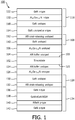
- Fig. 1 is a cross-sectional view of an epitaxial structure 100 for integrating GaN LEDs with AlGaN/GaN devices on a silicon (Si) substrate 102 in one or more embodiments of the present disclosure.
- GaN is not well suited for direct epitaxial growth on Si substrates due to the fact that Ga and Si form an eutectic material that destroys the Si substrate
- an undoped aluminum nitride (A1N) buffer layer 104 is first formed over a first side 105 of silicon substrate 102 (e.g., a topside as shown) to serve as a barrier between GaN and silicon.
- a thin AlN buffer layer 104 e.g., 100 angstroms to 2 microns
- An undoped Al x Ga 1-x N layer 106 may be formed over undoped AlN buffer layer 104 to provide additional separation between Si and GaN.
- a strain engineered stack 108 may be formed over Al x Ga 1-x N layer 106. Strain engineered stack 108 accommodates the strain due to a thermal expansion difference between Si and GaN in structure 100. Strain engineered stack 108 includes an undoped or doped GaN layer 110 and an undoped or doped AlN strain-releasing layer 112 over GaN layer 110. GaN layer 110 of stack 108 is formed directly over Al x Ga 1-x N layer 106. A second strain engineered stack 108A (not shown) maybe formed over first engineered stack 108.
- GaN layer 114 is formed over AlN strain-releasing layer 112 of strain engineered stack 108 to separate strain engineered stack 108 from an AlGaN/GaN heterojunction stack 116.
- GaN layer 114 may be doped with n-type dopant such as iron (Fe) to increase its resistance.
- GaN layer 114 is a non-conducting layer which prevents lateral leakage current from any HFET formed in an AlGaN/GaN heterojunction stack 116 (described later) above GaN layer 114 when the HFET is turned off. Isolation trenches may be etched down to GaN layer 114 to electrically insulate devices formed above GaN layer 114.
- AlGaN/GaN heterojunction stack 116 is formed over GaN layer 114.
- AlGaN/GaN heterojunction stack 116 includes an undoped GaN layer 118, a heavily doped, n-type Al x Ga 1-x N layer 120 on undoped GaN layer 118, and a passivation layer 122 (e.g., an n-type GaN) over n-type Al x Ga 1-x N layer 120.
- Undoped GaN layer 118 of heterojunction stack 116 is directly over GaN layer 114.
- AlGaN/GaN heterojunction stack 116 may be further processed to form devices including HFETs and Schottky diodes.
- Additional circuit elements may be integrated with, or built in layers over, AlGaN/GaN heterojunction stack 116.
- a resistor may be made utilizing a semiconductor layer of AlGaN/GaN heterojunction stack 116 (e.g., GaN layer 118) by forming two metal contacts at a certain distance between them.
- a capacitor may be made of a dielectric layer (silicon dioxide or silicon nitride) deposited above AlGaN/GaN heterojunction stack 116 and sandwiched between two metal layers, and an inductor may be made by forming a long winding metal pattern atop a semiconductor layer of AlGaN/GaN heterojunction stack 116 (e.g., GaN layer 118).
- An undoped AlN buffer layer 124 is formed over a second side 125 of silicon substrate 102 to serve as a barrier layer between GaN and silicon.
- An undoped Al x Ga 1-x N layer 126 is formed over undoped AlN buffer layer 124 to provide stress relief due to difference in thermal expansion and lattice constants between GaN and Si.
- a strain engineered stack 128 may be formed over undoped Al x Ga 1-x N layer 126. Strain engineered stack 128 includes an undoped GaN layer 130 and an undoped AlN strain-releasing layer 132 over undoped GaN layer 130. Undoped GaN layer 130 of stack 128 is directly over Al x Ga 1-x N layer 126. The structure of strain engineered stack 128 may be repeated over another engineered stack 128.
- GaN LED stack 134 is formed over undoped AlN strain-releasing layer 132 of strain engineering stack 128.
- GaN LED stack 134 includes an n-type GaN layer 136, GaN/ In y Ga 1-y N multiple quantum well (MQW) layers 138 over n-type GaN layer 136, a p-type Al x Ga 1-x N layer 140 over GaN/ In y Ga 1-y N MQW layers 138, and a p-type GaN layer 142 over p-type Al x Ga 1-x N layer 140.
- MQW multiple quantum well
- Al x Ga 1-x N and In y Ga 1-y N in different layers may be of different compositions and may be generally indicated as AlGaN and InGaN, respectively.
- N-type GaN layer 136 of stack 134 is directly over undoped AlN strain-releasing layer 132.
- GaN LED stack 134 may be further processed to exposed areas of n-type GaN layer 136 and p-type GaN layer 142 for forming n- and p-contacts. Additional circuit elements may be integrated with, or built in layers over, GaN LED stack 134.
- GaN LED stack 134 is not formed over a non-conducting GaN layer like heterojunction stack 116 because LEDs are vertical devices so lateral leakage current is not of great concern.
- Fig. 2 is a cross-sectional view of an epitaxial structure 200 for integrating GaN LEDs with AlGaN/GaN devices on a sapphire substrate 202 in one or more embodiments of the present disclosure.
- An undoped buffer layer 204 is first formed over a first side 205 of sapphire substrate 202 (e.g., a topside as shown) to provide a seed for growing other layers.
- Undoped buffer layer 204 maybe composed of GaN or AIN.
- An undoped GaN layer 206 is next formed on undoped buffer layer 204.
- GaN layer 206 maybe doped with n-type dopant such as Fe to increase its resistance.
- GaN layer 206 is non-conducting so it prevents lateral leakage current from any HFET device above the layer when the HFET is turned off. Isolation trenches may be etched down to GaN layer 206 to electrically insulate devices formed above the layer.
- AlGaN/GaN heterojunction stack 116 (described earlier) is formed over GaN layer 206. Undoped GaN layer 118 of heterojunction stack 116 is directly over GaN layer 206. AlGaN/GaN heterojunction stack 116 may be further processed to form devices including HFETs and Schottky diodes. Additional circuit elements may be integrated with, or built in layers over, AlGaN/GaN heterojunction stack 116.
- Undoped nucleation layer 208 is formed over a second side 209 of sapphire substrate 202 (e.g., a backside as shown) to seed other layers.
- Undoped nucleation layer 208 may be composed of GaN or AlN.
- GaN LED stack 134 (described earlier) is formed over undoped nucleation layer 208.
- N-type GaN layer 136 of stack 134 is directly over undoped nucleation layer 208.
- GaN LED stack 134 may be further processed to exposed areas of n-type GaN layer 136 and p-type GaN layer 142 for forming n- and p-contacts. Additional circuit elements may be integrated with, or built in layers over, GaN LED stack 134.
- Fig. 3 is a cross-sectional view of an epitaxial structure 300 for integrating GaN LEDs with AlGaN/GaN devices on a silicon carbon (SiC) substrate 302 in one or more embodiments of the present disclosure.
- An undoped nucleation layer 304 is first formed over a first side 305 of SiC substrate 302 (e.g., a topside as shown) to seed other layers.
- Undoped nucleation layer 304 may be composed of AlN or Al x Ga 1-x N.
- An undoped GaN layer 306 is next formed on undoped nucleation layer 304.
- GaN layer 306 maybe doped with n-type dopant such Fe to increase its resistance.
- GaN layer 306 is non-conducting so it prevents lateral leakage current from any HFET device above the layer when the HFET is turned off. Isolation trenches may be etched down to GaN layer 306 to electrically insulate devices formed above the layer.
- AlGaN/GaN heterojunction stack 116 (described earlier) is formed over GaN layer 306. Undoped GaN layer 118 of heterojunction stack 116 is directly over GaN layer 306. AlGaN/GaN heterojunction stack 116 may be further processed to form devices including HFETs and Schottky diodes. Additional circuit elements may be integrated with, or built in layers over, AlGaN/GaN heterojunction stack 116.
- Undoped nucleation layer 308 is formed over a second side (e.g., a backside as shown) 309 of SiC substrate 302 to seed other layers.
- Undoped nucleation layer 308 may be composed of AlN or Al x Ga 1-x N.
- GaN LED stack 134 (described earlier) is formed over undoped nucleation layer 308.
- N-type GaN layer 136 of stack 134 is directly over undoped nucleation layer 308.
- GaN LED stack 134 may be further processed to expose areas of n-type GaN layer 136 and p-type GaN layer 142 for forming n- and p-contacts. Additional circuit elements may be integrated with, or built in layers over, GaN LED stack 134.
- Fig. 4 is a cross-sectional view of an epitaxial structure 400 for integrating GaN LEDs with AlGaN/GaN devices on a GaN substrate 402 in one or more embodiments of the present disclosure.
- An undoped GaN layer 404 may be formed on a first side 405 of GaN substrate 402 (e.g., a topside as shown).
- GaN layer 404 maybe doped with n-type dopant such Fe to increase its resistance.
- GaN layer 404 is non-conducting so it prevents lateral leakage current from any HFET device above the layer when the HFET is turned off. Isolation trenches may be etched down to GaN layer 404 to electrically insulate devices formed above the layer.
- AlGaN/GaN heterojunction stack 116 (described earlier) is formed over GaN layer 404. Undoped GaN layer 118 of heterojunction stack 116 is directly over GaN layer 404. AlGaN/GaN heterojunction stack 116 may be further processed to form devices including HFETs and Schottky diodes. Additional circuit elements may be integrated with, or built in layers over, AlGaN/GaN heterojunction stack 116.
- GaN LED stack 134 (described earlier) is formed on a second side 406 of GaN substrate 402 (e.g., a backside as shown). N-type GaN layer 136 of stack 134 is directly over GaN substrate 402. GaN LED stack 134 may be further processed to exposed areas of n-type GaN layer 136 and p-type GaN layer 142 for forming n- and p-contacts. Additional circuit elements may be integrated with, or built in layers over, GaN LED stack 134.
- Fig. 5 shows a cross-sectional view of a structure 500 resulting from structure 200 ( Fig. 2 ) undergoing additional processing to form an AlGaN/GaN HFETs 506 and an AlGaN/GaN Schottky diode 508 in one or more embodiments of the present disclosure.
- P-type GaN layer 142 in GaN LED stack 134 may be roughened to improve light extraction.
- a p-contact 501 is formed on p-type GaN layer 142.
- One or more portions of structure 200 are removed down into n-type GaN layer 136 to form an n-contact 502 for an LED in GaN LED stack 134.
- portion of layers 116, 206, 204, 202, and 208 may be removed to form n-contact 502.
- layers 206, 204 202, 208, and all layers of GaN LED stack 134 except p-type GaN layer 142 may be removed to form p-contact 501. Locating all contacts on one side of the device enables a flip-chip configuration.
- An isolation trench 504 is etched through AlGaN/GaN heterojunction stack 116, GaN layer 206, and GaN or AlN buffer layer 204 down to sapphire substrate 202 to electrically insulate an HFET 506 and a Schottky diode 508.
- HFET 506 and Schottky diode 508 are connected by interconnects (not shown) to form a driver circuit for the LED in GaN LED stack 134.
- Other circuit elements such as resistors, capacitors, and inductors may also be formed in AlGaN/GaN heterojunction stack 116.
- HFET 506 includes a gate 512 and a source 514 and a drain 516 on the opposite sides of gate 512.
- Gate 512 contacts n-type Al x Ga 1-x N layer 120, and source 514 and drain 516 contact undoped GaN layer 118.
- an opening is etched in n-type GaN passivation layer 122 and metal is deposited on n-type Al x Ga 1-x N layer 120.
- metal is deposited on n-type GaN passivation layer 122 and diffused down to undoped GaN layer 118 by annealing.
- Schottky diode 508 includes an anode electrode 518 and a cathode electrode 520.
- Anode electrode 518 contacts n-type Al x Ga 1-x N layer 120.
- an opening is etched in n-type GaN passivation layer 122 and metal is deposited on n-type Al x Ga 1-x N layer 120.
- Cathode electrode 520 contacts undoped GaN layer 118.
- metal is deposited on n-type GaN passivation layer 122 and diffused down to undoped GaN layer 118 by annealing.
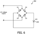
- Fig. 6 is a circuit diagram of a bridge rectifier circuit 602 connected to an LED 604.
- Bridge rectifier circuit 602 converts an AC voltage supply to DC voltage in order to power the LED in one or more embodiments of the present disclosure.
- Circuit 602 includes diodes D1, D2, D3, and D4 arranged in a typical diamond configuration where the cathode of diode D1 is connected to the anode of diode D2 and one side of the AC supply voltage, the cathode of diode D4 is connected to the anode of diode D3 and the other side of the AC supply voltage.
- the anodes of diodes D1 and D4 are the negative side of the rectified supply voltage for LED 604 and are connected to the cathode of LED 604.
- the cathodes of diodes D2 and D3 are the positive side of the rectified voltage and are connected to the anode of LED 604.
- Fig. 7 shows a cross-sectional view of a structure 700 resulting from structure 200 ( Fig. 2 ) undergoing additional processing to form bridge rectifier circuit 602 ( Fig. 6 ) in one or more embodiments of the present disclosure.
- Each diode in circuit 602 is implemented as an AlGaN/GaN Schottky diode in heterojunction stack 116.
- Diode D1 includes an anode electrode 702 and a cathode electrode 704.
- Diode D2 has an anode electrode 706 and shares a cathode electrode 708 with diode D3 because they are connected in series through undoped GaN layer 118.
- Diode D3 has an anode electrode 710 and cathode electrode 708.
- Diode D4 has an anode electrode 712 and a cathode electrode 714. Each anode electrode contacts n-type Al x Ga 1-x N layer 120, and each cathode electrode contacts undoped GaN layer 118. Diodes D1, D2, D3, and D4 are formed by the method described for forming diode 508 in structure 500 ( Fig. 5 ).
- Portions of AlGaN/GaN heterojunction stack 116, GaN layer 206, and GaN or AlN buffer layer 204 are removed to expose areas of sapphire substrate 202.
- an n-contact 722 is formed by etching an opening through sapphire substrate 202 and GaN or AlN buffer layer 208 and partially into n-type GaN layer 136 in GaN LED stack 134, and depositing metal in the opening.
- a p-contact 726 is formed by etching a hole through sapphire substrate 202, GaN or AlN buffer layer 208, and GaN LED stack 134, and depositing metal in the hole to contact p-type GaN layer 142 in GaN LED stack 134.
- the sidewalls of the holes for n-contact 722 and p-contact 726 are covered with an insulator such an oxide.
- the openings for n-contact 722 and p-contact 726 are each wide enough to allow a pillar of metal to be deposited without contacting the "sides" of the opening.
- a portion of p-type GaN layer 142 is left at the bottom of the opening and p-contact is 726 is deposited on the non-roughened surface of p-type GaN layer 142.
- Diodes D1, diodes D2, D3, and diodes D4 are electrically insulated from each other by isolation trenches 716.
- Isolation trenches 716 are etched through AlGaN/GaN heterojunction stack 116, GaN layer 206, and GaN or AlN buffer layer 204 down to sapphire substrate 202 to electrically insulate diodes D1, the pair of diodes D2, D3, and D4 from each other.
- Interconnects connect diodes D1, D2, D3, and D4 as shown in Fig. 6 .
- interconnects connect cathode electrode 708 (the cathodes of D2 and D3) to p-contact 726, the anode, of the LED in GaN LED stack 126, and anode electrodes 702 and 712 to n-contact 722, the cathode, of the LED in GaN LED stack 134.
- One side of the AC voltage is supplied to cathode electrode 704 of diode D1 and also to anode electrode 706 of diode D2.
- the other side of the AC voltage is supplied to anode electrode 710 of diode D3 and also to cathode electrode 714 of diode D4.
- Embodiments of the present disclosure offer the following advantages over the conventional LED-based light fixtures.
- the embodiments of the present disclosure integrate LEDs with the LED driver circuit on the same substrate template. Devices will be integrated on wafer-level with metal interconnects instead of the conventional method of making discrete LEDs and the LED driver circuit separately and then combining them at the die level.
- GaN transistor switches have lower specific-on-resistance than Si-based devices, providing less ohmic losses due to switching.
- the embodiments of the present disclosure have a smaller footprint.
- GaN transistors can handle higher operating voltage than Si-based devices so switching transistors can be made smaller.
- Necessary capacitors or inductors can also be made on wafer levels, thus reducing overall area.
- Die level interconnect such as wire bonding and soldering, is no longer needed between the LED driver circuit and LEDs as they are now done at wafer level.
- the embodiments of the present disclosure provide better temperature stability and prevent thermal runaway.
- LED current tends to have a positive temperature coefficient when driven at constant voltage because the LED's turn-on voltage becomes smaller when the LED warms up.
- FET field-effect transistor
- a field-effect transistor FET
- the embodiments of the present disclosure allow easier manufacturing for LED companies.
- An LED company may procure epitaxial wafers with AlGaN/GaN transistor structures grown on Si, sapphire, or SiC substrates from other companies and focus on improving LED structures on the other side of the substrates without worrying about optimizing the transistor structures.
- the thickness of the LED structures would not interfere with the transistor structures grown on the other side of the substrates. In other words, wafer processing of LEDs and transistors would not severely impact each other.
Landscapes
- Led Devices (AREA)
- Junction Field-Effect Transistors (AREA)
- Electrodes Of Semiconductors (AREA)
Claims (15)
- Procédé de fabrication d'une structure épitaxiale, comprenant :la fourniture d'un substrat (102, 202, 302, 402) et d'un empilement à hétérojonction (116) au-dessus d'un premier côté (105, 205, 305, 405) du substrat, l'empilement à hétérojonction comprenant une couche de nitrure de gallium GaN non dopée (118) au-dessus du premier côté du substrat et une couche de nitrure d'aluminium et de gallium AlGaN dopée (120) sur la couche de GaN non dopée ;la formation d'un empilement de diodes électroluminescentes de GaN (134) au-dessus d'un second côté (125, 209, 309, 406) du substrat, l'empilement de diodes électroluminescentes de GaN comprenant une couche de GaN de type n (136) au-dessus du second côté du substrat, une structure à puits quantiques multiples, MQW, de GaN/nitrure d'indium et de gallium, InGaN (138) au-dessus de la couche de GaN de type n, une couche d'AlGaN de type p (140) au-dessus de la structure MQW de GaN/InGaN de type n, et une couche de GaN de type p (142) au-dessus de la couche d'AlGaN de type p,et ensuite, le traitement de l'empilement à hétérojonction pour former un ou plusieurs dispositifs couplés électriquement à l'empilement de diodes électroluminescentes pour former un circuit d'excitation, les un ou plusieurs dispositifs incluant un ou plusieurs d'un transistor à effet de champ à hétérojonction HFET d'AlGaN/GaN (506) et d'une diode de Schottky d'AlGaN/GaN (508).
- Procédé selon la revendication 1, dans lequel :le substrat est un substrat de silicium (102) ;la fourniture du substrat et de l'empilement à hétérojonction au-dessus du premier côté (105) du substrat comprend :la formation d'un premier empilement conçu sous contrainte (108) au-dessus du premier côté du substrat,le premier empilement conçu sous contrainte incorporant une contrainte entre le silicium et le GaN ; etla formation de l'empilement à hétérojonction au-dessus du premier empilement conçu sous contrainte ; etle procédé comprend en outre la formation d'un second empilement conçu sous contrainte (128) au-dessus du second côté (125) du substrat, l'empilement de diodes électroluminescentes de GaN (134) étant formé au-dessus du second empilement conçu sous contrainte ; et dans lequelle premier empilement conçu sous contrainte (108) comprend :une première couche de GaN (110) au-dessus du premier côté (105) du substrat ; etune première couche de libération de contrainte de nitrure d'aluminium AlN (112) sur la première couche de GaN ; etle second empilement conçu sous contrainte (128) comprend :une seconde couche de GaN (130) au-dessus du second côté (205) du substrat ; etune seconde couche de libération de contrainte d'AlN (132) sur la seconde couche de GaN.
- Procédé selon la revendication 2, comprenant en outre :la formation d'une première couche tampon d'AlN non dopée (104) au-dessus du premier côté (105) du substrat ; etla formation d'une première couche d'AlGaN non dopée (106) au-dessus de la première couche tampon d'AlN non dopée (104), le premier empilement conçu sous contrainte (108) étant formé au-dessus de la première couche d'AlGaN non dopée (106) ;la formation d'une seconde couche tampon d'AlN non dopée (124) au-dessus du second côté (125) du substrat ; etla formation d'une seconde couche d'AlGaN non dopée (126) au-dessus de la seconde couche tampon d'AlN non dopée (124), le second empilement conçu sous contrainte (128) étant formé au-dessus de la seconde couche d'AlGaN non dopée (126).
- Procédé selon la revendication 3, comprenant en outre :
entre le premier empilement conçu sous contrainte (108) et l'empilement à hétérojonction (116), la formation d'une couche de GaN non conductrice (114). - Procédé selon la revendication 1, dans lequel le substrat comprend un substrat de saphir (202), le procédé comprenant en outre :la formation d'une première couche de nucléation de GaN ou AlN (204) au-dessus du premier côté (205) du substrat ; etla formation d'une couche de GaN non conductrice (206) au-dessus de la couche de nucléation de GaN ou d'AlN (204), l'empilement à hétérojonction (116) étant formé au-dessus de la couche de GaN non conductrice (206) ; etla formation d'une seconde couche de nucléation de GaN ou d'AlN (208) au-dessus du second côté (209) du substrat, l'empilement de diodes électroluminescentes de GaN (134) étant formé au-dessus de la seconde couche tampon de GaN ou d'AlN (208).
- Procédé selon la revendication 1, dans lequel le substrat comprend un substrat de carbure de silicium, SiC (302), le procédé comprenant en outre :la formation d'une première couche de nucléation d'AlN ou AlGaN (304) au-dessus du premier côté (305) du substrat ;la formation d'une couche de GaN non conductrice (306) au-dessus de la première couche de nucléation d'AlN ou d'AlGaN (304), l'empilement à hétérojonction (116) étant formé au-dessus de la couche de GaN non conductrice (306) ; etla formation d'une seconde couche de nucléation d'AlN ou d'AlGaN (308) au-dessus du second côté (309) du substrat, l'empilement de diodes électroluminescentes de GaN (134) étant formé au-dessus de la seconde couche de nucléation d'AlN ou d'AlGaN (308).
- Procédé selon la revendication 1, dans lequel le substrat comprend un substrat de GaN (402), le procédé comprenant en outre :
la formation d'une couche de GaN non conductrice (404) au-dessus du premier côté (405) du substrat, l'empilement à hétérojonction (116) étant formé au-dessus de la couche de GaN non conductrice (404). - Procédé selon la revendication 1, dans lequel ledit traitement de l'empilement à hétérojonction (116) comprend :la formation d'une source (514) pour le HFET d'AlGaN/GaN (506) qui est en contact avec la couche de GaN non dopée (118) ;la formation d'un drain (516) pour le HFET d'AlGaN/GaN (506) qui est en contact avec la couche de GaN non dopée (118) ;la formation d'une grille (512) pour le HFET d'AlGaN/GaN (506) qui est en contact avec la couche d'AlGaN dopée (120) ;la formation d'une anode (518) pour la diode de Schottky d'AlGaN/GaN (508) qui est en contact avec la couche d'AlGaN dopée (120) ; etla formation d'une cathode (520) pour la diode de Schottky d'AlGaN/GaN (508) qui est en contact avec la couche de GaN non dopée (118).
- Structure épitaxiale, comprenant :un substrat (102, 202, 302, 402) ;un empilement à hétérojonction (116) au-dessus d'un premier côté (105, 205, 305, 405) du substrat, l'empilement à hétérojonction comprenant une couche de GaN non dopée (118) au-dessus du premier côté du substrat et une couche d'AlGaN dopée (120) sur la couche de GaN non dopée ;un empilement de diodes électroluminescentes de GaN (134) au-dessus d'un second côté (125, 209, 309, 406) du substrat, l'empilement de diodes électroluminescentes de GaN comprenant une couche de GaN de type n (136) au-dessus du second côté du substrat, une structure MQW de GaN/InGaN (138) au-dessus de la couche de GaN de type n, une couche d'AlGaN de type p (140) au-dessus de la structure MQW de GaN/InGaN de type n, et une couche de GaN de type p (142) au-dessus de la couche d'AlGaN de type p,dans laquelle l'empilement à hétérojonction comprend un ou plusieurs dispositifs couplés électriquement à l'empilement de diodes électroluminescentes pour former un circuit d'excitation, les un ou plusieurs dispositifs incluant un ou plusieurs d'un transistor à effet de champ à hétérojonction HFET d'AlGaN/GaN (506) et d'une diode de Schottky d'AlGaN/GaN (508).
- Structure selon la revendication 11, dans laquelle le substrat est un substrat de silicium (102), la structure comprenant en outre :un premier empilement conçu sous contrainte (108) au-dessus du premier côté (105) du substrat, le premier empilement conçu sous contrainte incorporant une contrainte entre le silicium et le GaN, l'empilement à hétérojonction se trouvant au-dessus du premier empilement conçu sous contrainte ; etun second empilement conçu sous contrainte (128) au-dessus du second côté (125) du substrat, l'empilement de diodes électroluminescentes de GaN (134) se trouvant au-dessus du second empilement conçu sous contrainte, le premier empilement conçu sous contrainte (108) comprenant :une première couche de GaN (110) au-dessus du premier côté (105) du substrat ; etune première couche de libération de contrainte de nitrure d'aluminium AlN (112) sur la première couche de GaN ; etle second empilement sous contrainte (128) comprenant :une seconde couche de GaN (130) au-dessus du second côté (205) du substrat ; etune seconde couche de libération de contrainte d'AlN (132) sur la seconde couche de GaN.
- Structure selon la revendication 10, comprenant en outre :une première couche tampon d'AlN non dopée (104) au-dessus du premier côté (105) du substrat ; etune première couche d'AlGaN non dopée (106) au-dessus de la première couche tampon d'AlN non dopée, le premier empilement conçu sous contrainte (108) étant au-dessus de la première couche d'AlGaN non dopée (106) ;une seconde couche tampon d'AlN non dopée (124) au-dessus du second côté (125) du substrat ;une seconde couche d'AlGaN non dopée (126) au-dessus de la seconde couche tampon d'AlN non dopée (124), l'empilement de diodes électroluminescentes de GaN (134) se trouvant au-dessus de la seconde couche d'AlGaN non dopée (126), etune couche de GaN non conductrice (114) au-dessus du premier empilement conçu sous contrainte (108), l'empilement à hétérojonction (116) se trouvant au-dessus de la première couche de GaN non conductrice (114).
- Structure selon la revendication 9, dans laquelle le substrat comprend un substrat de saphir (202), la structure comprenant en outre :une première couche de nucléation de GaN ou AlN (204) au-dessus du premier côté (205) du substrat ; etune couche de GaN non conductrice (206) au-dessus de la couche de nucléation de GaN ou d'AlN (204), l'empilement à hétérojonction (116) se trouvant au-dessus de la couche de GaN non conductrice (206) ; etune seconde couche de nucléation de GaN ou d'AlN (208) au-dessus du second côté (209) du substrat, l'empilement de diodes électroluminescentes de GaN (134) se trouvant au-dessus de la seconde couche de nucléation de GaN ou d'AlN (208).
- Structure selon la revendication 9, dans laquelle le substrat comprend un substrat de SiC (302), la structure comprenant en outre :une première couche de nucléation d'AlN ou AlGaN (304) au-dessus du premier côté (305) du substrat ;une couche de GaN non conductrice (306) au-dessus de la première couche de nucléation d'AlN ou d'AlGaN (304), l'empilement à hétérojonction (116) se trouvant au-dessus de la couche de GaN non conductrice (306) ; etune seconde couche de nucléation d'AlN ou d'AlGaN (308) au-dessus du second côté (309) du substrat, l'empilement de diodes électroluminescentes de GaN (134) se trouvant au-dessus de la seconde couche de nucléation d'AlN ou d'AlGaN (308).
- Structure selon la revendication 11, dans laquelle le substrat comprend un substrat de GaN (402), la structure comprenant en outre :
une couche de GaN non conductrice (404) au-dessus du premier côté (405) du substrat, l'empilement à hétérojonction (116) se trouvant au-dessus de la couche de GaN non conductrice (404). - Structure selon la revendication 9, dans laquelle l'empilement à hétérojonction (116) comprend :une source (514) pour le HFET d'AlGaN/GaN (506) qui est en contact avec la couche de GaN non dopée (118) ;un drain (516) pour le HFET d'AlGaN/GaN (506) qui est en contact avec la couche de GaN non dopée (118) ;une grille (512) pour le HFET d'AlGaN/GaN (506) qui est en contact avec la couche d'AlGaN dopée (120) ;une anode (518) pour la diode de Schottky d'AlGaN/GaN (508) qui est en contact avec la couche d'AlGaN dopée (120) ; etune cathode (520) pour la diode de Schottky d'AlGaN/GaN (508) qui est en contact avec la couche de GaN non dopée (118).
Applications Claiming Priority (2)
| Application Number | Priority Date | Filing Date | Title |
|---|---|---|---|
| US201261603985P | 2012-02-28 | 2012-02-28 | |
| PCT/IB2013/051613 WO2013128410A1 (fr) | 2012-02-28 | 2013-02-28 | Intégration de diodes électroluminescentes au nitrure de gallium (del) à des dispositifs au nitrure de gallium-nitrure d'aluminium-gallium sur des substrats en silicium pour del en courant alternatif |
Publications (2)
| Publication Number | Publication Date |
|---|---|
| EP2820678A1 EP2820678A1 (fr) | 2015-01-07 |
| EP2820678B1 true EP2820678B1 (fr) | 2019-05-08 |
Family
ID=48182957
Family Applications (1)
| Application Number | Title | Priority Date | Filing Date |
|---|---|---|---|
| EP13718387.7A Active EP2820678B1 (fr) | 2012-02-28 | 2013-02-28 | Intégration de diodes électroluminescentes au nitrure de gallium (del) à des dispositifs au nitrure de gallium-nitrure d'aluminium-gallium sur des substrats en silicium pour del en courant alternatif |
Country Status (8)
| Country | Link |
|---|---|
| US (1) | US9054232B2 (fr) |
| EP (1) | EP2820678B1 (fr) |
| JP (1) | JP6316210B2 (fr) |
| KR (1) | KR102032437B1 (fr) |
| CN (1) | CN104170089B (fr) |
| RU (1) | RU2615215C2 (fr) |
| TW (1) | TWI591846B (fr) |
| WO (1) | WO2013128410A1 (fr) |
Families Citing this family (30)
| Publication number | Priority date | Publication date | Assignee | Title |
|---|---|---|---|---|
| US9660043B2 (en) | 2012-06-04 | 2017-05-23 | Sensor Electronic Technology, Inc. | Ohmic contact to semiconductor layer |
| US9793439B2 (en) * | 2012-07-12 | 2017-10-17 | Sensor Electronic Technology, Inc. | Metallic contact for optoelectronic semiconductor device |
| FR3024010A1 (fr) * | 2014-07-17 | 2016-01-22 | Commissariat Energie Atomique | Dispositif incluant une diode electroluminescente et un transformateur associe |
| WO2016074642A1 (fr) | 2014-11-14 | 2016-05-19 | The Hong Kong University Of Science And Technology | Transistors à source de photons intégrée sur puce ou à drain photonique-ohmique pour faciliter la libération d'électrons piégés dans des pièges profonds de transistors |
| TWI577046B (zh) * | 2014-12-23 | 2017-04-01 | 錼創科技股份有限公司 | 半導體發光元件及其製作方法 |
| CN106299095A (zh) * | 2015-06-12 | 2017-01-04 | 映瑞光电科技(上海)有限公司 | 一种高压倒装led芯片及其制作方法 |
| CN107615491B (zh) * | 2015-10-09 | 2021-05-14 | 美国休斯研究所 | 蓝宝石上氮化镓单片集成功率变换器 |
| CN105445854B (zh) | 2015-11-06 | 2018-09-25 | 南京邮电大学 | 硅衬底悬空led光波导集成光子器件及其制备方法 |
| WO2017096032A1 (fr) * | 2015-12-04 | 2017-06-08 | Quora Technology, Inc. | Architecture de circuit intégré pour dispositif à large bande interdite sur substrat modifié |
| CN105938864B (zh) * | 2016-06-22 | 2018-05-29 | 厦门乾照光电股份有限公司 | 一种ac-led芯片及其制造方法 |
| JP6825251B2 (ja) * | 2016-07-12 | 2021-02-03 | 富士ゼロックス株式会社 | 発光素子 |
| TWI605552B (zh) | 2016-12-08 | 2017-11-11 | 新唐科技股份有限公司 | 半導體元件、半導體基底及其形成方法 |
| CN107195801B (zh) * | 2017-05-22 | 2019-08-16 | 茆胜 | 一种oled微型显示器及其阳极键合方法 |
| US11069834B2 (en) * | 2017-09-18 | 2021-07-20 | King Abdullah University Of Science And Technology | Optoelectronic device having a boron nitride alloy electron blocking layer and method of production |
| US10748881B2 (en) * | 2017-12-05 | 2020-08-18 | Seoul Viosys Co., Ltd. | Light emitting device with LED stack for display and display apparatus having the same |
| CN108198835A (zh) * | 2017-12-07 | 2018-06-22 | 黎子兰 | 一种led显示单元、显示器及其制造方法 |
| FR3077160B1 (fr) * | 2018-01-19 | 2022-01-21 | Commissariat Energie Atomique | Dispositif optoelectronique comportant une grille et une cathode couplees l'une a l'autre |
| JP2019161172A (ja) * | 2018-03-16 | 2019-09-19 | 株式会社ブイ・テクノロジー | Led・トランジスタ複合素子 |
| US10201051B1 (en) * | 2018-04-10 | 2019-02-05 | Nthdegree Technologies Worldwide Inc. | Active LED module with LED and vertical MOS transistor formed on same substrate |
| KR102778196B1 (ko) * | 2019-10-17 | 2025-03-10 | 삼성전자주식회사 | 구동소자를 포함하는 발광소자 및 그 제조방법 |
| US11569182B2 (en) | 2019-10-22 | 2023-01-31 | Analog Devices, Inc. | Aluminum-based gallium nitride integrated circuits |
| KR102767850B1 (ko) | 2019-11-19 | 2025-02-14 | 삼성전자주식회사 | 반도체 구조체, 이를 포함하는 트랜지스터 및 트랜지스터의 제조방법 |
| CN111710692A (zh) * | 2020-06-19 | 2020-09-25 | 中国工程物理研究院电子工程研究所 | 一种led与hfet的集成外延片及其选区移除方法 |
| CN112054130B (zh) * | 2020-09-19 | 2021-11-02 | 福州大学 | 基于交流电场驱动半导体pn结的可拉伸发光器件及其方法 |
| LV15627B (lv) | 2020-09-30 | 2023-07-20 | Storm Adventures, Sia | Horizontāls vēja tunelis |
| TWI808759B (zh) * | 2022-05-13 | 2023-07-11 | 天光材料科技股份有限公司 | 電極連接結構及其形成方法 |
| CN115548012B (zh) * | 2022-09-26 | 2025-10-17 | 山东大学 | 一种高可靠AlGaN/GaN HEMT及其制备方法 |
| CN115863382B (zh) * | 2023-02-27 | 2023-06-06 | 长沙湘计海盾科技有限公司 | 一种新型GaN外延结构及其制备方法和应用 |
| KR102668094B1 (ko) * | 2023-03-13 | 2024-05-22 | 웨이브로드 주식회사 | 칼라필터가 불필요한 수직 적층형 마이크로디스플레이 패널 및 그 제조 방법 |
| KR102655449B1 (ko) * | 2023-11-24 | 2024-04-09 | 주식회사 멤스 | 쇼트키 다이오드 및 이의 형성 방법 |
Family Cites Families (23)
| Publication number | Priority date | Publication date | Assignee | Title |
|---|---|---|---|---|
| JPH0793419B2 (ja) * | 1992-11-04 | 1995-10-09 | 日本電気株式会社 | 受光発光集積素子 |
| JPH11214800A (ja) * | 1998-01-28 | 1999-08-06 | Sony Corp | 半導体装置およびその製造方法 |
| JP3709077B2 (ja) | 1998-07-21 | 2005-10-19 | シャープ株式会社 | 半導体レーザ装置およびその製造方法、並びに、ピックアップ装置 |
| JP2002305327A (ja) * | 2001-04-09 | 2002-10-18 | Sharp Corp | 窒化物系半導体発光素子 |
| TW492202B (en) * | 2001-06-05 | 2002-06-21 | South Epitaxy Corp | Structure of III-V light emitting diode (LED) arranged in flip chip configuration having structure for preventing electrostatic discharge |
| JP2003086784A (ja) * | 2001-09-13 | 2003-03-20 | Furukawa Electric Co Ltd:The | GaN系半導体装置 |
| TWI243399B (en) * | 2003-09-24 | 2005-11-11 | Sanken Electric Co Ltd | Nitride semiconductor device |
| TWI229463B (en) * | 2004-02-02 | 2005-03-11 | South Epitaxy Corp | Light-emitting diode structure with electro-static discharge protection |
| JP4189386B2 (ja) | 2005-01-27 | 2008-12-03 | ローム株式会社 | 窒化物半導体結晶層の成長方法および窒化物半導体発光素子の製法 |
| JP2007243006A (ja) * | 2006-03-10 | 2007-09-20 | Kyocera Corp | 窒化物系半導体の気相成長方法、及び、エピタキシャル基板とそれを用いた半導体装置 |
| JP2007305959A (ja) * | 2006-04-10 | 2007-11-22 | Seiko Epson Corp | 光素子およびその製造方法 |
| US7534638B2 (en) * | 2006-12-22 | 2009-05-19 | Philips Lumiled Lighting Co., Llc | III-nitride light emitting devices grown on templates to reduce strain |
| US7547908B2 (en) * | 2006-12-22 | 2009-06-16 | Philips Lumilieds Lighting Co, Llc | III-nitride light emitting devices grown on templates to reduce strain |
| JP2009071220A (ja) * | 2007-09-18 | 2009-04-02 | Toyoda Gosei Co Ltd | Iii族窒化物系化合物半導体発光素子 |
| US8076699B2 (en) * | 2008-04-02 | 2011-12-13 | The Hong Kong Univ. Of Science And Technology | Integrated HEMT and lateral field-effect rectifier combinations, methods, and systems |
| US20090261346A1 (en) | 2008-04-16 | 2009-10-22 | Ding-Yuan Chen | Integrating CMOS and Optical Devices on a Same Chip |
| JP2010080955A (ja) * | 2008-08-29 | 2010-04-08 | Toshiba Corp | 半導体装置 |
| EP3163601B1 (fr) * | 2009-01-23 | 2020-03-11 | Nichia Corporation | Procédé de fabrication d'un dispositif à semiconducteur par connexion directe d'argent sur une surface d'un composant à semiconducteur avec oxyde d'argent sur une surface d'une base |
| US8338837B2 (en) | 2009-06-08 | 2012-12-25 | Epistar Corporation | Light emitting device |
| JP4681684B1 (ja) * | 2009-08-24 | 2011-05-11 | Dowaエレクトロニクス株式会社 | 窒化物半導体素子およびその製造方法 |
| CN102117771B (zh) | 2009-12-31 | 2013-05-08 | 比亚迪股份有限公司 | 一种发光二极管外延片和管芯及其制作方法 |
| JP2012023280A (ja) * | 2010-07-16 | 2012-02-02 | Seiwa Electric Mfg Co Ltd | 半導体発光素子、発光装置、照明装置、表示装置、信号灯器及び道路情報装置 |
| US9252330B2 (en) * | 2010-08-06 | 2016-02-02 | Panasonic Intellectual Property Management Co., Ltd. | Semiconductor light emitting element |
-
2013
- 2013-02-28 WO PCT/IB2013/051613 patent/WO2013128410A1/fr not_active Ceased
- 2013-02-28 US US14/378,113 patent/US9054232B2/en active Active
- 2013-02-28 RU RU2014138822A patent/RU2615215C2/ru not_active IP Right Cessation
- 2013-02-28 CN CN201380011427.5A patent/CN104170089B/zh active Active
- 2013-02-28 EP EP13718387.7A patent/EP2820678B1/fr active Active
- 2013-02-28 JP JP2014558266A patent/JP6316210B2/ja active Active
- 2013-02-28 KR KR1020147027229A patent/KR102032437B1/ko active Active
- 2013-03-01 TW TW102107416A patent/TWI591846B/zh not_active IP Right Cessation
Non-Patent Citations (1)
| Title |
|---|
| None * |
Also Published As
| Publication number | Publication date |
|---|---|
| KR102032437B1 (ko) | 2019-10-16 |
| US9054232B2 (en) | 2015-06-09 |
| WO2013128410A1 (fr) | 2013-09-06 |
| US20150014628A1 (en) | 2015-01-15 |
| TW201347228A (zh) | 2013-11-16 |
| TWI591846B (zh) | 2017-07-11 |
| JP2015508238A (ja) | 2015-03-16 |
| KR20140136012A (ko) | 2014-11-27 |
| EP2820678A1 (fr) | 2015-01-07 |
| CN104170089A (zh) | 2014-11-26 |
| CN104170089B (zh) | 2017-05-31 |
| JP6316210B2 (ja) | 2018-04-25 |
| RU2014138822A (ru) | 2016-04-20 |
| RU2615215C2 (ru) | 2017-04-04 |
Similar Documents
| Publication | Publication Date | Title |
|---|---|---|
| EP2820678B1 (fr) | Intégration de diodes électroluminescentes au nitrure de gallium (del) à des dispositifs au nitrure de gallium-nitrure d'aluminium-gallium sur des substrats en silicium pour del en courant alternatif | |
| US7842974B2 (en) | Gallium nitride heterojunction schottky diode | |
| US10499475B2 (en) | LED driver and illumination system related to the same | |
| TWI525753B (zh) | 利用島狀形貌之氮化鎵功率器件 | |
| KR101922122B1 (ko) | 노멀리 오프 고전자이동도 트랜지스터 | |
| US8552471B2 (en) | Semiconductor apparatus having reverse blocking characteristics and method of manufacturing the same | |
| KR101919422B1 (ko) | 질화물 반도체 기반의 파워 변환 장치 | |
| CN103367356B (zh) | 具有氮化物层的半导体元件 | |
| US9231093B2 (en) | High electron mobility transistor and method of manufacturing the same | |
| US9231056B2 (en) | Semiconductor device and fabrication method therefor, and power supply apparatus | |
| US8426895B2 (en) | Semiconductor device and manufacturing method of the same | |
| JP2015043414A (ja) | 高電圧iv族イナーブルスイッチを備えるモノリシック複合iii族窒化物トランジスタ | |
| US20120043588A1 (en) | Semiconductor device | |
| CN103579329A (zh) | 高电子迁移率晶体管及其制造方法 | |
| JP5643783B2 (ja) | Iii−v族トランジスタとiv族ダイオードを含む積層複合デバイス | |
| WO2014108945A1 (fr) | Dispositif semi-conducteur au nitrure | |
| Lu et al. | High performance monolithically integrated GaN driving VMOSFET on LED | |
| KR20130031690A (ko) | 파워 소자 및 그 제조 방법 | |
| KR101871712B1 (ko) | 질화물계 반도체 이종접합 반도체 소자 및 그 제조방법 | |
| KR20150044326A (ko) | 쇼트키 배리어 다이오드가 일체화된 고전자 이동도 트랜지스터를 구비하는 반도체 소자 및 그 제조 방법 | |
| WO2023082203A1 (fr) | Dispositif semi-conducteur à base de nitrure et son procédé de fabrication | |
| CN108696959B (zh) | 发光二极管的驱动器 | |
| KR20150016667A (ko) | 질화물계 전계효과 트랜지스터 및 그 제조방법 |
Legal Events
| Date | Code | Title | Description |
|---|---|---|---|
| PUAI | Public reference made under article 153(3) epc to a published international application that has entered the european phase |
Free format text: ORIGINAL CODE: 0009012 |
|
| 17P | Request for examination filed |
Effective date: 20140929 |
|
| AK | Designated contracting states |
Kind code of ref document: A1 Designated state(s): AL AT BE BG CH CY CZ DE DK EE ES FI FR GB GR HR HU IE IS IT LI LT LU LV MC MK MT NL NO PL PT RO RS SE SI SK SM TR |
|
| AX | Request for extension of the european patent |
Extension state: BA ME |
|
| DAX | Request for extension of the european patent (deleted) | ||
| RAP1 | Party data changed (applicant data changed or rights of an application transferred) |
Owner name: LUMILEDS HOLDING B.V. |
|
| GRAP | Despatch of communication of intention to grant a patent |
Free format text: ORIGINAL CODE: EPIDOSNIGR1 |
|
| STAA | Information on the status of an ep patent application or granted ep patent |
Free format text: STATUS: GRANT OF PATENT IS INTENDED |
|
| INTG | Intention to grant announced |
Effective date: 20181218 |
|
| RAP1 | Party data changed (applicant data changed or rights of an application transferred) |
Owner name: LUMILEDS HOLDING B.V. |
|
| GRAS | Grant fee paid |
Free format text: ORIGINAL CODE: EPIDOSNIGR3 |
|
| GRAA | (expected) grant |
Free format text: ORIGINAL CODE: 0009210 |
|
| STAA | Information on the status of an ep patent application or granted ep patent |
Free format text: STATUS: THE PATENT HAS BEEN GRANTED |
|
| AK | Designated contracting states |
Kind code of ref document: B1 Designated state(s): AL AT BE BG CH CY CZ DE DK EE ES FI FR GB GR HR HU IE IS IT LI LT LU LV MC MK MT NL NO PL PT RO RS SE SI SK SM TR |
|
| REG | Reference to a national code |
Ref country code: GB Ref legal event code: FG4D |
|
| REG | Reference to a national code |
Ref country code: CH Ref legal event code: EP Ref country code: AT Ref legal event code: REF Ref document number: 1131575 Country of ref document: AT Kind code of ref document: T Effective date: 20190515 |
|
| REG | Reference to a national code |
Ref country code: DE Ref legal event code: R096 Ref document number: 602013054992 Country of ref document: DE Ref country code: IE Ref legal event code: FG4D |
|
| REG | Reference to a national code |
Ref country code: NL Ref legal event code: MP Effective date: 20190508 |
|
| REG | Reference to a national code |
Ref country code: LT Ref legal event code: MG4D |
|
| PG25 | Lapsed in a contracting state [announced via postgrant information from national office to epo] |
Ref country code: LT Free format text: LAPSE BECAUSE OF FAILURE TO SUBMIT A TRANSLATION OF THE DESCRIPTION OR TO PAY THE FEE WITHIN THE PRESCRIBED TIME-LIMIT Effective date: 20190508 Ref country code: HR Free format text: LAPSE BECAUSE OF FAILURE TO SUBMIT A TRANSLATION OF THE DESCRIPTION OR TO PAY THE FEE WITHIN THE PRESCRIBED TIME-LIMIT Effective date: 20190508 Ref country code: FI Free format text: LAPSE BECAUSE OF FAILURE TO SUBMIT A TRANSLATION OF THE DESCRIPTION OR TO PAY THE FEE WITHIN THE PRESCRIBED TIME-LIMIT Effective date: 20190508 Ref country code: AL Free format text: LAPSE BECAUSE OF FAILURE TO SUBMIT A TRANSLATION OF THE DESCRIPTION OR TO PAY THE FEE WITHIN THE PRESCRIBED TIME-LIMIT Effective date: 20190508 Ref country code: NO Free format text: LAPSE BECAUSE OF FAILURE TO SUBMIT A TRANSLATION OF THE DESCRIPTION OR TO PAY THE FEE WITHIN THE PRESCRIBED TIME-LIMIT Effective date: 20190808 Ref country code: PT Free format text: LAPSE BECAUSE OF FAILURE TO SUBMIT A TRANSLATION OF THE DESCRIPTION OR TO PAY THE FEE WITHIN THE PRESCRIBED TIME-LIMIT Effective date: 20190908 Ref country code: SE Free format text: LAPSE BECAUSE OF FAILURE TO SUBMIT A TRANSLATION OF THE DESCRIPTION OR TO PAY THE FEE WITHIN THE PRESCRIBED TIME-LIMIT Effective date: 20190508 Ref country code: ES Free format text: LAPSE BECAUSE OF FAILURE TO SUBMIT A TRANSLATION OF THE DESCRIPTION OR TO PAY THE FEE WITHIN THE PRESCRIBED TIME-LIMIT Effective date: 20190508 Ref country code: NL Free format text: LAPSE BECAUSE OF FAILURE TO SUBMIT A TRANSLATION OF THE DESCRIPTION OR TO PAY THE FEE WITHIN THE PRESCRIBED TIME-LIMIT Effective date: 20190508 |
|
| PG25 | Lapsed in a contracting state [announced via postgrant information from national office to epo] |
Ref country code: BG Free format text: LAPSE BECAUSE OF FAILURE TO SUBMIT A TRANSLATION OF THE DESCRIPTION OR TO PAY THE FEE WITHIN THE PRESCRIBED TIME-LIMIT Effective date: 20190808 Ref country code: RS Free format text: LAPSE BECAUSE OF FAILURE TO SUBMIT A TRANSLATION OF THE DESCRIPTION OR TO PAY THE FEE WITHIN THE PRESCRIBED TIME-LIMIT Effective date: 20190508 Ref country code: LV Free format text: LAPSE BECAUSE OF FAILURE TO SUBMIT A TRANSLATION OF THE DESCRIPTION OR TO PAY THE FEE WITHIN THE PRESCRIBED TIME-LIMIT Effective date: 20190508 Ref country code: GR Free format text: LAPSE BECAUSE OF FAILURE TO SUBMIT A TRANSLATION OF THE DESCRIPTION OR TO PAY THE FEE WITHIN THE PRESCRIBED TIME-LIMIT Effective date: 20190809 |
|
| REG | Reference to a national code |
Ref country code: AT Ref legal event code: MK05 Ref document number: 1131575 Country of ref document: AT Kind code of ref document: T Effective date: 20190508 |
|
| PG25 | Lapsed in a contracting state [announced via postgrant information from national office to epo] |
Ref country code: EE Free format text: LAPSE BECAUSE OF FAILURE TO SUBMIT A TRANSLATION OF THE DESCRIPTION OR TO PAY THE FEE WITHIN THE PRESCRIBED TIME-LIMIT Effective date: 20190508 Ref country code: SK Free format text: LAPSE BECAUSE OF FAILURE TO SUBMIT A TRANSLATION OF THE DESCRIPTION OR TO PAY THE FEE WITHIN THE PRESCRIBED TIME-LIMIT Effective date: 20190508 Ref country code: AT Free format text: LAPSE BECAUSE OF FAILURE TO SUBMIT A TRANSLATION OF THE DESCRIPTION OR TO PAY THE FEE WITHIN THE PRESCRIBED TIME-LIMIT Effective date: 20190508 Ref country code: DK Free format text: LAPSE BECAUSE OF FAILURE TO SUBMIT A TRANSLATION OF THE DESCRIPTION OR TO PAY THE FEE WITHIN THE PRESCRIBED TIME-LIMIT Effective date: 20190508 Ref country code: RO Free format text: LAPSE BECAUSE OF FAILURE TO SUBMIT A TRANSLATION OF THE DESCRIPTION OR TO PAY THE FEE WITHIN THE PRESCRIBED TIME-LIMIT Effective date: 20190508 Ref country code: CZ Free format text: LAPSE BECAUSE OF FAILURE TO SUBMIT A TRANSLATION OF THE DESCRIPTION OR TO PAY THE FEE WITHIN THE PRESCRIBED TIME-LIMIT Effective date: 20190508 |
|
| REG | Reference to a national code |
Ref country code: DE Ref legal event code: R097 Ref document number: 602013054992 Country of ref document: DE |
|
| PG25 | Lapsed in a contracting state [announced via postgrant information from national office to epo] |
Ref country code: SM Free format text: LAPSE BECAUSE OF FAILURE TO SUBMIT A TRANSLATION OF THE DESCRIPTION OR TO PAY THE FEE WITHIN THE PRESCRIBED TIME-LIMIT Effective date: 20190508 Ref country code: IT Free format text: LAPSE BECAUSE OF FAILURE TO SUBMIT A TRANSLATION OF THE DESCRIPTION OR TO PAY THE FEE WITHIN THE PRESCRIBED TIME-LIMIT Effective date: 20190508 |
|
| PLBE | No opposition filed within time limit |
Free format text: ORIGINAL CODE: 0009261 |
|
| STAA | Information on the status of an ep patent application or granted ep patent |
Free format text: STATUS: NO OPPOSITION FILED WITHIN TIME LIMIT |
|
| PG25 | Lapsed in a contracting state [announced via postgrant information from national office to epo] |
Ref country code: TR Free format text: LAPSE BECAUSE OF FAILURE TO SUBMIT A TRANSLATION OF THE DESCRIPTION OR TO PAY THE FEE WITHIN THE PRESCRIBED TIME-LIMIT Effective date: 20190508 |
|
| 26N | No opposition filed |
Effective date: 20200211 |
|
| PG25 | Lapsed in a contracting state [announced via postgrant information from national office to epo] |
Ref country code: PL Free format text: LAPSE BECAUSE OF FAILURE TO SUBMIT A TRANSLATION OF THE DESCRIPTION OR TO PAY THE FEE WITHIN THE PRESCRIBED TIME-LIMIT Effective date: 20190508 |
|
| PG25 | Lapsed in a contracting state [announced via postgrant information from national office to epo] |
Ref country code: SI Free format text: LAPSE BECAUSE OF FAILURE TO SUBMIT A TRANSLATION OF THE DESCRIPTION OR TO PAY THE FEE WITHIN THE PRESCRIBED TIME-LIMIT Effective date: 20190508 |
|
| REG | Reference to a national code |
Ref country code: CH Ref legal event code: PL |
|
| REG | Reference to a national code |
Ref country code: BE Ref legal event code: MM Effective date: 20200229 |
|
| PG25 | Lapsed in a contracting state [announced via postgrant information from national office to epo] |
Ref country code: LU Free format text: LAPSE BECAUSE OF NON-PAYMENT OF DUE FEES Effective date: 20200228 Ref country code: MC Free format text: LAPSE BECAUSE OF FAILURE TO SUBMIT A TRANSLATION OF THE DESCRIPTION OR TO PAY THE FEE WITHIN THE PRESCRIBED TIME-LIMIT Effective date: 20190508 |
|
| PG25 | Lapsed in a contracting state [announced via postgrant information from national office to epo] |
Ref country code: LI Free format text: LAPSE BECAUSE OF NON-PAYMENT OF DUE FEES Effective date: 20200229 Ref country code: CH Free format text: LAPSE BECAUSE OF NON-PAYMENT OF DUE FEES Effective date: 20200229 |
|
| PG25 | Lapsed in a contracting state [announced via postgrant information from national office to epo] |
Ref country code: IE Free format text: LAPSE BECAUSE OF NON-PAYMENT OF DUE FEES Effective date: 20200228 |
|
| PG25 | Lapsed in a contracting state [announced via postgrant information from national office to epo] |
Ref country code: BE Free format text: LAPSE BECAUSE OF NON-PAYMENT OF DUE FEES Effective date: 20200229 |
|
| PG25 | Lapsed in a contracting state [announced via postgrant information from national office to epo] |
Ref country code: MT Free format text: LAPSE BECAUSE OF FAILURE TO SUBMIT A TRANSLATION OF THE DESCRIPTION OR TO PAY THE FEE WITHIN THE PRESCRIBED TIME-LIMIT Effective date: 20190508 Ref country code: CY Free format text: LAPSE BECAUSE OF FAILURE TO SUBMIT A TRANSLATION OF THE DESCRIPTION OR TO PAY THE FEE WITHIN THE PRESCRIBED TIME-LIMIT Effective date: 20190508 |
|
| PG25 | Lapsed in a contracting state [announced via postgrant information from national office to epo] |
Ref country code: MK Free format text: LAPSE BECAUSE OF FAILURE TO SUBMIT A TRANSLATION OF THE DESCRIPTION OR TO PAY THE FEE WITHIN THE PRESCRIBED TIME-LIMIT Effective date: 20190508 Ref country code: IS Free format text: LAPSE BECAUSE OF FAILURE TO SUBMIT A TRANSLATION OF THE DESCRIPTION OR TO PAY THE FEE WITHIN THE PRESCRIBED TIME-LIMIT Effective date: 20190908 |
|
| P01 | Opt-out of the competence of the unified patent court (upc) registered |
Effective date: 20230530 |
|
| REG | Reference to a national code |
Ref country code: DE Ref legal event code: R079 Ref document number: 602013054992 Country of ref document: DE Free format text: PREVIOUS MAIN CLASS: H01L0027150000 Ipc: H10H0029140000 |
|
| PGFP | Annual fee paid to national office [announced via postgrant information from national office to epo] |
Ref country code: GB Payment date: 20260223 Year of fee payment: 14 |
|
| PGFP | Annual fee paid to national office [announced via postgrant information from national office to epo] |
Ref country code: DE Payment date: 20260220 Year of fee payment: 14 |
|
| PGFP | Annual fee paid to national office [announced via postgrant information from national office to epo] |
Ref country code: FR Payment date: 20260224 Year of fee payment: 14 |