EP2822026B1 - Verbundsubstrat - Google Patents
Verbundsubstrat Download PDFInfo
- Publication number
- EP2822026B1 EP2822026B1 EP13754726.1A EP13754726A EP2822026B1 EP 2822026 B1 EP2822026 B1 EP 2822026B1 EP 13754726 A EP13754726 A EP 13754726A EP 2822026 B1 EP2822026 B1 EP 2822026B1
- Authority
- EP
- European Patent Office
- Prior art keywords
- intermediate layer
- semiconductor layer
- supporting substrate
- substrate
- layer
- Prior art date
- Legal status (The legal status is an assumption and is not a legal conclusion. Google has not performed a legal analysis and makes no representation as to the accuracy of the status listed.)
- Not-in-force
Links
Images


Classifications
-
- H—ELECTRICITY
- H10—SEMICONDUCTOR DEVICES; ELECTRIC SOLID-STATE DEVICES NOT OTHERWISE PROVIDED FOR
- H10D—INORGANIC ELECTRIC SEMICONDUCTOR DEVICES
- H10D86/00—Integrated devices formed in or on insulating or conducting substrates, e.g. formed in silicon-on-insulator [SOI] substrates or on stainless steel or glass substrates
- H10D86/201—Integrated devices formed in or on insulating or conducting substrates, e.g. formed in silicon-on-insulator [SOI] substrates or on stainless steel or glass substrates the substrates comprising an insulating layer on a semiconductor body, e.g. SOI
-
- H—ELECTRICITY
- H10—SEMICONDUCTOR DEVICES; ELECTRIC SOLID-STATE DEVICES NOT OTHERWISE PROVIDED FOR
- H10D—INORGANIC ELECTRIC SEMICONDUCTOR DEVICES
- H10D30/00—Field-effect transistors [FET]
- H10D30/60—Insulated-gate field-effect transistors [IGFET]
- H10D30/67—Thin-film transistors [TFT]
- H10D30/6704—Thin-film transistors [TFT] having supplementary regions or layers in the thin films or in the insulated bulk substrates for controlling properties of the device
-
- H—ELECTRICITY
- H10—SEMICONDUCTOR DEVICES; ELECTRIC SOLID-STATE DEVICES NOT OTHERWISE PROVIDED FOR
- H10D—INORGANIC ELECTRIC SEMICONDUCTOR DEVICES
- H10D30/00—Field-effect transistors [FET]
- H10D30/60—Insulated-gate field-effect transistors [IGFET]
- H10D30/67—Thin-film transistors [TFT]
- H10D30/674—Thin-film transistors [TFT] characterised by the active materials
- H10D30/6741—Group IV materials, e.g. germanium or silicon carbide
- H10D30/6743—Silicon
- H10D30/6744—Monocrystalline silicon
-
- H—ELECTRICITY
- H10—SEMICONDUCTOR DEVICES; ELECTRIC SOLID-STATE DEVICES NOT OTHERWISE PROVIDED FOR
- H10D—INORGANIC ELECTRIC SEMICONDUCTOR DEVICES
- H10D30/00—Field-effect transistors [FET]
- H10D30/60—Insulated-gate field-effect transistors [IGFET]
- H10D30/67—Thin-film transistors [TFT]
- H10D30/6758—Thin-film transistors [TFT] characterised by the insulating substrates
-
- H—ELECTRICITY
- H10—SEMICONDUCTOR DEVICES; ELECTRIC SOLID-STATE DEVICES NOT OTHERWISE PROVIDED FOR
- H10P—GENERIC PROCESSES OR APPARATUS FOR THE MANUFACTURE OR TREATMENT OF DEVICES COVERED BY CLASS H10
- H10P14/00—Formation of materials, e.g. in the shape of layers or pillars
- H10P14/20—Formation of materials, e.g. in the shape of layers or pillars of semiconductor materials
- H10P14/29—Formation of materials, e.g. in the shape of layers or pillars of semiconductor materials characterised by the substrates
- H10P14/2901—Materials
- H10P14/2921—Materials being crystalline insulating materials
-
- H—ELECTRICITY
- H10—SEMICONDUCTOR DEVICES; ELECTRIC SOLID-STATE DEVICES NOT OTHERWISE PROVIDED FOR
- H10P—GENERIC PROCESSES OR APPARATUS FOR THE MANUFACTURE OR TREATMENT OF DEVICES COVERED BY CLASS H10
- H10P14/00—Formation of materials, e.g. in the shape of layers or pillars
- H10P14/20—Formation of materials, e.g. in the shape of layers or pillars of semiconductor materials
- H10P14/32—Formation of materials, e.g. in the shape of layers or pillars of semiconductor materials characterised by intermediate layers between substrates and deposited layers
- H10P14/3202—Materials thereof
- H10P14/3204—Materials thereof being Group IVA semiconducting materials
- H10P14/3211—Silicon, silicon germanium or germanium
-
- H—ELECTRICITY
- H10—SEMICONDUCTOR DEVICES; ELECTRIC SOLID-STATE DEVICES NOT OTHERWISE PROVIDED FOR
- H10P—GENERIC PROCESSES OR APPARATUS FOR THE MANUFACTURE OR TREATMENT OF DEVICES COVERED BY CLASS H10
- H10P14/00—Formation of materials, e.g. in the shape of layers or pillars
- H10P14/20—Formation of materials, e.g. in the shape of layers or pillars of semiconductor materials
- H10P14/32—Formation of materials, e.g. in the shape of layers or pillars of semiconductor materials characterised by intermediate layers between substrates and deposited layers
- H10P14/3202—Materials thereof
- H10P14/3238—Materials thereof being insulating materials
-
- H—ELECTRICITY
- H10—SEMICONDUCTOR DEVICES; ELECTRIC SOLID-STATE DEVICES NOT OTHERWISE PROVIDED FOR
- H10P—GENERIC PROCESSES OR APPARATUS FOR THE MANUFACTURE OR TREATMENT OF DEVICES COVERED BY CLASS H10
- H10P14/00—Formation of materials, e.g. in the shape of layers or pillars
- H10P14/20—Formation of materials, e.g. in the shape of layers or pillars of semiconductor materials
- H10P14/32—Formation of materials, e.g. in the shape of layers or pillars of semiconductor materials characterised by intermediate layers between substrates and deposited layers
- H10P14/3202—Materials thereof
- H10P14/3241—Materials thereof being conductive materials
-
- H—ELECTRICITY
- H10—SEMICONDUCTOR DEVICES; ELECTRIC SOLID-STATE DEVICES NOT OTHERWISE PROVIDED FOR
- H10P—GENERIC PROCESSES OR APPARATUS FOR THE MANUFACTURE OR TREATMENT OF DEVICES COVERED BY CLASS H10
- H10P90/00—Preparation of wafers not covered by a single main group of this subclass, e.g. wafer reinforcement
- H10P90/19—Preparing inhomogeneous wafers
- H10P90/1904—Preparing vertically inhomogeneous wafers
- H10P90/1906—Preparing SOI wafers
- H10P90/1914—Preparing SOI wafers using bonding
-
- H—ELECTRICITY
- H10—SEMICONDUCTOR DEVICES; ELECTRIC SOLID-STATE DEVICES NOT OTHERWISE PROVIDED FOR
- H10P—GENERIC PROCESSES OR APPARATUS FOR THE MANUFACTURE OR TREATMENT OF DEVICES COVERED BY CLASS H10
- H10P14/00—Formation of materials, e.g. in the shape of layers or pillars
- H10P14/20—Formation of materials, e.g. in the shape of layers or pillars of semiconductor materials
- H10P14/32—Formation of materials, e.g. in the shape of layers or pillars of semiconductor materials characterised by intermediate layers between substrates and deposited layers
- H10P14/3242—Structure
- H10P14/3244—Layer structure
- H10P14/3248—Layer structure consisting of two layers
-
- H—ELECTRICITY
- H10—SEMICONDUCTOR DEVICES; ELECTRIC SOLID-STATE DEVICES NOT OTHERWISE PROVIDED FOR
- H10P—GENERIC PROCESSES OR APPARATUS FOR THE MANUFACTURE OR TREATMENT OF DEVICES COVERED BY CLASS H10
- H10P14/00—Formation of materials, e.g. in the shape of layers or pillars
- H10P14/20—Formation of materials, e.g. in the shape of layers or pillars of semiconductor materials
- H10P14/32—Formation of materials, e.g. in the shape of layers or pillars of semiconductor materials characterised by intermediate layers between substrates and deposited layers
- H10P14/3242—Structure
- H10P14/3244—Layer structure
- H10P14/3251—Layer structure consisting of three or more layers
Definitions
- the present invention relates to a composite substrate having a semiconductor layer.
- SOS silicon on sapphire
- As a method of forming the SOS structure there is a technique disclosed in Japanese Unexamined Patent Application Publication No. 2003-31781 , for example.
- As a method of bonding a substrate made of a different material there is a technique described in Japanese Unexamined Patent Application Publication No. 2004-343369 , for example.
- Document EP1858071 A1 discloses a composite substrate comprising a sapphire substrate and an alumina intermediate layer and a semiconductor layer.
- US 2006/0051554 A1 discloses a substrate comprising a sapphire substrate, an alumina intermediate layer and a semiconductor layer.
- a composite substrate includes a supporting substrate, a semiconductor layer, and an intermediate layer.
- the supporting substrate is composed of sapphire.
- the semiconductor layer is composed of a single crystal and bonded to the supporting substrate such that a main surface of the semiconductor layer faces to the supporting substrate.
- the intermediate layer is disposed between the supporting substrate and the semiconductor layer.
- the intermediate layer includes alumina as a main component and a sub-component as further specified in claim 1.
- the intermediate layer is composed of a polycrystal or an amorphous material.
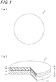
- a composite substrate 1 includes a supporting substrate 10, a semiconductor layer 20, and an intermediate layer 30.
- the intermediate layer 30 is disposed between the supporting substrate 10 and the semiconductor layer 20.
- the intermediate layer 30 includes an element contained in the supporting substrate 10 or the semiconductor layer 20 as a main component.
- An existence amount of a sub-component other than a main component is equal to or less than 1 mass%.
- the intermediate layer 30 has significantly high purity, and is different from a so-called glass material.
- the positional relationship between the supporting substrate 10, the intermediate layer 30, and the semiconductor layer 20 is common in the examples and the embodiments described below.
- a composite substrate 1A is configured to include a supporting substrate 10A, the semiconductor layer 20, and an intermediate layer 30A.
- the supporting substrate 10A may support the semiconductor layer 20 which is disposed at an upper portion thereof, may include a desired strength and a desired flatness of a surface, and may contain oxygen.
- a material contained in the supporting substrate 10A it is possible to use an aluminum oxide single crystal (sapphire), quartz, a resin substrate, or the like. It can be freely select crystallinity or the like of the supporting substrate 10A, but the example employs a single crystal sapphire as the supporting substrate 10A.
- Examples of a thickness of the supporting substrate 10A include a range of 400 [ ⁇ m] to 800 [ ⁇ m].
- the semiconductor layer 20 is bonded to the supporting substrate 10A such that a main surface 20b faces to a main surface 10a.
- a single crystal semiconductor material may be used, for example, it is possible to use Si, Ge, GaAs, ZnTe, GaN, an organic semiconductor single crystal, or the like. In the example, an Si single crystal is used as the semiconductor layer 20.
- Examples of a thickness of the semiconductor layer 20 include a range of 30 [nm] to 200 [nm].
- an example of dopant concentration of the semiconductor layer 20 includes concentrations of p - and n - , which mean relatively low concentrations, and non-doped, and the semiconductor layer 20 is formed to be any one of those described above.
- Examples of the concentration of p - include a range which is equal to or less than 1 ⁇ 10 16 [atoms/cm 3 ].
- Examples of the concentration of n - include a range which is equal to or less than 5 ⁇ 10 15 [atoms/cm 3 ].
- a “non-doped silicon” is a silicon which is not doped, simply intending impurities, and is not limited to an intrinsic silicon which does not include the impurities. It is preferable that the oxygen concentration in the semiconductor layer 20 be equal to or less than the oxygen concentration of an interface of the semiconductor layer 20 side of the intermediate layer 30 which will be described later. The oxygen concentration will be described in detail, but may be less than 1 ⁇ 10 18 [atoms/cm 3 ].
- the intermediate layer 30A is disposed between the supporting substrate 10 and the semiconductor layer 20.
- One main surface of the intermediate layer 30A is directly bonded to the supporting substrate 10A, and the other main surface is directly bonded to the semiconductor layer 20.
- the intermediate layer 30A is in a state where a crystal structure of both of the supporting substrate 10A and the semiconductor layer 20 is disturbed.
- an element of a main component contained in the supporting substrate 10A that is, alumina
- an element contained in the semiconductor layer 20, that is, Si both exist individually as elemental substances.
- the element contained in the supporting substrate 10A and the element contained in the semiconductor layer 20 are not chemically combined.
- the intermediate layer 30A contains the element of the main component contained in the supporting substrate 10A, the intermediate layer 30A contains oxygen on the inside thereof.
- the interface between the intermediate layer 30A and supporting substrate 10A can be determined by a difference in the crystal structure.
- the supporting substrate 10A is present up to an area which is the single crystal, and the intermediate layer 30A is present from an area in which the crystal structure is disturbed.
- the interface between the intermediate layer 30A and the semiconductor layer 20 can also be similarly determined.
- the crystallinity of the intermediate layer 30A is low compared to that of the supporting substrate 10A and the semiconductor layer 20.
- the intermediate layer 30A is composed of a pseudo-polycrystal made of two types of crystal structures which is different from the single crystal and in which the crystal structure that constitutes the supporting substrate 10A and the crystal structure that constitutes the semiconductor layer 20 are mixed.
- the difference in the crystallinity may be recognized by observing with a transmission electron microscope (TEM), for example, after forming cross-section with focusing ion beam (FIB) processing, or by performing electron beam diffraction.
- TEM transmission electron microscope
- FIB focusing ion beam
- RBS Rutherford backscattering
- a combining method is different from a general method of combining both of these via a bonding layer.
- the intermediate layer 30A includes an oxygen concentration distribution in which the oxygen concentration decreases as the intermediate layer 30A approaches the semiconductor layer 20.
- a state of the oxygen concentration distribution in the intermediate layer 30A is not particularly limited, but may be inclined to be the same as the oxygen concentration of the semiconductor layer 20 in the interface between the semiconductor layer 20 and the intermediate layer 30A.
- the thickness of the intermediate layer 30A be equal to or less than 50 [nm]. More preferably, the thickness of the intermediate layer 30A is 5 [nm] to 10 [nm]. This is because parasitic capacitance or heat conduction is not adversely influenced, even in a case of a layer other than the single crystal, for example, a layer including oxygen, by having such a thickness described above.
- the composite substrate 1A is configured in this manner, it is possible to suppress the diffusion and the deposition of the impurities to the semiconductor layer 20. Hereinafter, the reason thereof will be described.
- the impurities such as a metal
- the impurities which are contained in an significantly small amount to the supporting substrate 10A, diffused to the semiconductor layer 20 and are deposited.
- the presence of the metal causes an occurrence of a malfunction when an element function portion which functions as the semiconductor device is configured in the semiconductor layer 20.
- the impurities, such as the metal it is important to prevent the diffusion and the deposition to the semiconductor layer 20.
- the intermediate layer 30A is provided on the composite substrate 1A.
- the metal has less combining energy of combining with oxygen.
- Si and Fe contained in the semiconductor layer 20 are taken as an example, a eutectic temperature of Si-Fe is 660[°C]. While heating is required in the combination, the combination of Fe-O is processed even at a room temperature. For this reason, the metal does not diffuse to the semiconductor layer 20, combines with oxygen of the intermediate layer 30A, and is maintained inside the intermediate layer 30A.
- the oxygen concentration of the intermediate layer 30A decreases as approaching the semiconductor layer 20, it is possible to maintain the metal on the supporting substrate 10A in the thickness direction of the intermediate layer 30A without leaving the metal on the interface between the semiconductor layer 20 and the intermediate layer 30A.
- the semiconductor layer 20 is the single crystal, and from this point of view, it is possible to incorporate the metal into the intermediate layer 30A in which the diffusion and the solid dissolution easily occur.
- the oxygen concentration of the semiconductor layer 20 is less than 1 ⁇ 10 18 [atoms/cm 3 ]. According to this configuration, the diffusion, the solid dissolution, and the deposition of the metal to the semiconductor layer 20 are suppressed. In particular, when the metal is Fe, it is possible to suppress the occurrence of an OSF defect.
- the composite substrate 1 it is possible to provide a semiconductor layer 20 having a high quality in which the diffusion of the impurities, such as the metal, to the semiconductor layer 20 is suppressed.
- an intermediate layer 30B which further contains metallic atoms existing as an elemental substance may be used.
- the metallic atoms can include Fe, Cr, Ni, Cu, Zn, or the like.
- the element of the main component contained in the supporting substrate 10A and the semiconductor layer 20 is excluded.
- the content is as specified in claim 1 and further discussed in paragraphs [0150]-[0161]. It is important that the metallic element is contained as an elemental substance. In other words, it is important that the metallic element is not combined with the element contained in the supporting substrate 10A and the semiconductor layer 20, and is maintained as an elemental substance in a defective area where the crystal of the element contained in the supporting substrate 10A and semiconductor layer 20 is disturbed.
- the metallic element since the metallic element is not directly related to the combination, the metallic element does not exist in a layer shape on the interface of the semiconductor layer 20 side. As a result, it is possible to suppress the diffusion to the semiconductor layer 20. In addition, even when the metallic atoms cause a new reaction or the diffusion due to a heat treatment for forming the semiconductor device, it is possible to suppress the exfoliation of the semiconductor layer 20, and to enhance the reliability, without influencing the combining strength. Furthermore, as the metallic element exists as an elemental substance inside the intermediate layer 30B, it is possible to keep the new reaction and a phenomenon, such as the diffusion, inside the intermediate layer 30B even when the heat treatment or the like for forming the semiconductor device is performed.
- the metallic element can be moved to the supporting substrate 10A by the following heat treatment or the like.
- the concentration of the metallic element it is preferable that the concentration of the metallic element be distributed in the thickness direction, and the concentration decrease from the supporting substrate 10A.
- the composite substrate 1A it is possible to achieve a good reliability without deteriorating a characteristic of the semiconductor layer 20 even with respect to the following heat treatment.
- the metallic element is not combined with the supporting substrate 10A and the semiconductor layer 20, even if a distortion due to a heat history or the like added to the composite substrate 1A occurs, the metallic element can move to mitigate the distortion.
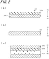
- a first substrate 20X formed of silicon (Si) is prepared.
- the first substrate 20X is made by forming an Si film 20Xb which epitaxially grows Si on an upper surface (D2 direction in the drawing) of the single crystal silicon substrate 20Xa.
- a part of the Si film 20Xb later becomes semiconductor layer 20.
- the epitaxial growth method it is possible to employ various methods, such as a heat chemical vapor deposition method (heat CVD method) which passes into, thermally decomposes, and grows a gaseous silicon compound on a surface of the single crystal silicon substrate 20Xa, while heating the single crystal silicon substrate 20Xa.
- heat CVD method heat chemical vapor deposition method
- the Si film 20Xb is epitaxially grown on the silicon substrate, it is possible to reduce a lattice defect compared to in a case where the Si film 20Xb is epitaxially grown on the sapphire substrate.
- the film is epitaxially grown in a vacuum, it is possible to suppress the oxygen content in the film to be significantly low compared to in the silicon substrate formed by a CZ method. More particularly, it is possible to make the oxygen concentration to be less than 10 18 [atoms/cm 3 ].
- the oxygen concentration is a value which is equal to or less than 1/10 compared to in the silicon substrate formed by the CZ method. Practically, it is verified that the oxygen concentration can be less than 3 ⁇ 10 17 [atoms/cm 3 ].
- the dopant concentration of the Si film 20Xb is not particularly limited, but for example, is the p-type dopant concentration and the n-type dopant concentration which are relatively low concentrations, and the film is formed to be any one of non-doped films.
- the p-type dopant concentration include a range which is equal to or less than 1 ⁇ 10 16 [atoms/cm 3 ].
- the n-type dopant concentration include a range which is equal to or less than 5 ⁇ 10 15 [atoms/cm 3 ].
- the dopant concentration of the Si film 20Xb decreases from the single crystal silicon substrate 20Xa, and becomes the dopant concentration which is a completely depleted layer on the surface of a side opposite to the side which is in contact with the single crystal silicon substrate 20Xa.
- the thickness of the Si film 20Xb be approximately 2 [ ⁇ m], for example.
- the insulating supporting substrate 10A which is composed of the aluminum oxide single crystal (sapphire) is prepared.
- the supporting substrate 10A and a main surface (main surface which is positioned on a side opposite to the single crystal silicon substrate 20Xa) of the first substrate 20X in a D1 direction are bonded to each other.
- the supporting substrate 10A and the main surface of the Si film 20Xb are bonded to each other.
- Examples of a method of bonding, as illustrated in Fig. 2(c) include a method of bonding by activating the surface of the bonded surface, and a method of bonding by using an electrostatic force.
- Examples of a method of activating the surface include a method of activating by irradiating the surface with the ion beam or the neutron beam in a vacuum and etching the surface, and a method of activating by etching the surface by a chemical solution.
- the intermediate layer 30A As illustrated in Fig. 3(a) , by applying a pressure in an activated state, it is possible to form the intermediate layer 30A in a state where a crystal of a part of the interface between the supporting substrate 10A and the Si film 20Xb is disturbed.
- the thickness of the intermediate layer 30A, the ratio of the element contained in the supporting substrate 10A, and the ratio of the element contained in the Si film 20Xb By adjusting an extent and an aggravation of the activation of the surface by the output of the ion beam and the neutron beam, it is possible to control the thickness of the intermediate layer 30A, the ratio of the element contained in the supporting substrate 10A, and the ratio of the element contained in the Si film 20Xb.
- the metal is prevented from being floated in a bonding apparatus so that the metal is not interposed as the bonding layer on the bonding surface.
- a metal generating source is covered by a cover member which is made of ceramic, the inside of the bonding apparatus is cleaned, or a degree of vacuum is ensured.
- the bonding may be performed at a room temperature.
- the bonding is performed by a method in which an adhesive, such as a resin-based adhesive, is not used.
- the Si film 20Xb and the supporting substrate 10A have small surface roughness of the surface to be bonded.
- the surface roughness is represented by an arithmetic average roughness Ra or a root mean square Rq, for example.
- Examples of a range of the arithmetic average roughness Ra include a range which is less than 10 [nm].
- Examples of a range of the root mean square Rq include a range which is less than 5 [nm].
- the intermediate product is processed from the arrow D1 direction side (single crystal silicon substrate 20Xa side), and the Si film 20Xb is exposed by removing the single crystal silicon substrate 20Xa as illustrated in Fig. 3(b) .
- a processing method of removing the single crystal silicon substrate 20Xa for example, it is possible to employ various methods, such as an abrasive grain polishing, a chemical etching, or an ion beam etching, and a plurality of methods may be combined.
- a part of the Si film 20Xb may be removed in the thickness direction together with the single crystal silicon substrate 20Xa.
- the single crystal silicon substrate 20Xa be removed by using a substrate having a high dopant concentration as the single crystal silicon substrate 20Xa, and by using an etchant in which an etching rate in the dopant concentration of the single crystal silicon substrate 20Xa and an etching rate in the dopant concentration of the Si film 20Xb are largely different from each other.
- productivity can increase, and the Si film 20Xb can remain on the surface of the main surface 10a of the supporting substrate 10 with a uniform thickness, for example, even when a wave of the supporting substrate 10 is large.
- etching means which is used in the precise etching include a dry etching.
- the dry etching include an etching according to a chemical reaction and an etching according to a physical collision.
- the etching which uses the chemical reaction include an etching which uses reactive gas, a reactive ion and ion beam, and a reactive radical, or the like.
- the etching gas which is used in the reactive ion include sulfur hexafluoride (SF 6 ) or carbon tetrafluoride (CF 4 ).
- examples of the physical collision include an etching which uses the ion beam.
- examples of the etching which uses the ion beam include a method of using a gas cluster ion beam (GCIB). While etching a narrow area by using the etching means, it is possible to perform the precise etching well even in a case of a base material substrate having a large area, by scanning the substrate in a movable stage.
- GCIB gas cluster ion beam
- a remaining part of the Si film 20Xb after proceeding the process is considered as the semiconductor layer 20.
- the entire process proceeds in this manner, it is possible to obtain the composite substrate 1A which is stacked in an order of intermediate layer 30A and the semiconductor layer 20 on the supporting substrate 10A.
- the surface of the supporting substrate 10A of the semiconductor layer 20 which is formed by the epitaxial growth becomes a non-doped depleted layer, and the oxygen concentration also decreases.
- the distortion of the surface of the supporting substrate 10A of the semiconductor layer 20 becomes significantly small. This configuration is preferable since a stress or the like is not applied by the unintended distortion on the surface of the bonding with the supporting substrate 10A.
- an SiOx layer (oxide layer) having a constant film thickness like an SOI substrate in the related art does not exist between the supporting substrate 10A and the semiconductor layer 20, particularly, on the semiconductor layer 20.
- the layer in which the oxygen is the main component and the semiconductor layer 20 are not in contact with each other, and it is possible to realize the bonding with the supporting substrate 10A. According to this, it is possible to suppress an occurrence of the unintended stress which is required to form the SiOx layer, and an occurrence of interstitial Si or the like, in the semiconductor layer 20, and to improve the quality of the semiconductor layer 20.
- the substrate may be cleaned if necessary.
- a method of cleaning the substrate include various methods, such as cleaning by using an ultrasonic wave, cleaning by using an organic solvent, cleaning by using chemicals, and cleaning by using O 2 ashing. These methods of cleaning may be combined with each other and used.
- the composite substrate 1C is different in a supporting substrate 10C and an intermediate layer 30C.
- the positional relationship between the supporting substrate 10C, the intermediate layer 30C, and the semiconductor layer 20 is the same as that between the supporting substrate 10, the intermediate layer 30, and the semiconductor layer 20 of the composite substrate 1, as illustrated in Fig. 1 .
- the repeating description will be omitted.
- the supporting substrate 10C supports the semiconductor layer 20 which is disposed on an upper portion thereof.
- the sapphire which is an insulating material is employed as the supporting substrate 10C.
- Examples of a thickness of the supporting substrate 10C include a range from 400 [ ⁇ m] to 800 [ ⁇ m]. In addition, it is preferable that the arithmetic average roughness Ra of the supporting substrate 10C be equal to or less than 1 [nm].
- the intermediate layer 30C is disposed between the supporting substrate 10C and the semiconductor layer 20.
- the intermediate layer 30C has alumina as the main component.
- the crystallinity of the intermediate layer 30C is low compared to that of the supporting substrate 10C.
- the intermediate layer 30C is composed of a polycrystal or an amorphous material.
- the thickness of the intermediate layer 30C is is set to be able to solid-dissolve the amount of the metal which causes a concern that the metal is incorporated by bonding the supporting substrate 10C and the semiconductor layer 20 to each other, which will be described later.
- a melting point of alumina is approximately 1800[°C].
- the metal which exists on the interface between the intermediate layer 30C and the supporting substrate 10C does not react to the element contained in the intermediate layer 30C, or is not encouraged to diffuse. For this reason, the above-described maximum value of the thickness is not necessarily required.
- the thickness equal to or less than 50 [nm]. More preferably, the thickness may be equal to or less than 10 [nm].
- One main surface of the intermediate layer 30C is directly bonded to the supporting substrate 10C, and the other main surface is directly bonded to the semiconductor layer 20.
- a boundary between the intermediate layer 30C and the supporting substrate 10C can be determined by the difference in the crystal structure.
- the supporting substrate 10C is present up to an area which is the single crystal, and the intermediate layer 30C is present from an area in which the crystal structure is disturbed.
- the composite substrate 1C is configured in this manner, it is possible to suppress the diffusion or the deposition of the impurities to the semiconductor layer 20. Hereinafter, the reason thereof will be described.
- the intermediate layer 30C is provided on the composite substrate 1C.
- the intermediate layer 30C is configured by the same material-based element as the element contained in the supporting substrate 10C.
- the intermediate layer 30C is an alumina layer.
- the melting point of alumina is high, and alumina is not combined with the metal and does not encourage the diffusion of the metal even when the metal exists. For this reason, the metal which exists on the interface between the supporting substrate 10C and the intermediate layer 30C is maintained between the supporting substrate 10C and the intermediate layer 30C, and as a result, it is possible to suppress the diffusion of the metal to the semiconductor layer 20.
- the crystallinity of the intermediate layer 30C is low compared to that of the single crystal semiconductor layer 20 and the supporting substrate 10C. For this reason, the metal does not diffuse to the semiconductor layer 20, and the metal diffuses and is solid-dissolved to the intermediate layer 30C via a grain boundary or the like.
- the evaluation of the crystallinity of the intermediate layer 30C may be conducted by observing by using the transmission electron microscope (TEM), for example, after the cross-section processing by the focusing ion beam (FIB) processing, and by performing the electron beam diffraction.
- TEM transmission electron microscope
- FIB focusing ion beam
- RBS Rutherford backscattering
- an oxygen amount per unit volume of the intermediate layer 30C is small compared to the supporting substrate 10C, and accordingly, it is possible to suppress the combination of the metal and the oxygen, and to suppress the movement according to the diffusion of the metal.
- the composite substrate 1C it is possible to suppress the diffusion of the impurities, such as the metal, to the semiconductor layer 20, and to provide the semiconductor layer 20 having a high quality.
- an intermediate layer 30D in which the crystal structure changes in the thickness direction may be used.
- the intermediate layer 30D is composed of a polycrystal including alumina. A ratio of ⁇ alumina increases while the intermediate layer 30D goes toward the supporting substrate 10C in the thickness direction, and a ratio of ⁇ alumina increases while the intermediate layer 30D goes toward the semiconductor layer 20.
- the middle of the thickness of the intermediate layer 30D is in a state where the crystal structure is the most disturbed. Accordingly, if the metal exists, it is possible to maintain the metal by considering the middle of the thickness of the intermediate layer 30D as the center.
- the supporting substrate 10C since the crystal structure which is exposed to one main surface of the supporting substrate 10C becomes close to a cubic crystal, preferably, a consistency with the intermediate layer 30D having a high proportion of ⁇ alumina on the supporting substrate 10C side becomes good.
- an intermediate layer 30E which further includes the metallic element is used.
- the metallic element can include Fe, Cr, Ni, Cu, Zn, or the like.
- the element of the main component contained in the supporting substrate 10 and the semiconductor layer 20 is excluded.
- the content in a vicinity of the interface with the supporting substrate is equal to or greater than 1 x 10 10 atoms /cm 2 and equal to or less than 1 x 10 12 atoms / cm 2 . Further details are found in paragraphs [0150] - [0155] and [0160].
- the concentration of the metallic element in the intermediate layer 30E decreases from the supporting substrate 10C toward the semiconductor layer 20 in the thickness direction. According to this configuration, it is possible to reliably prevent the metallic element from diffusing to the semiconductor layer 20.
- a manufacturing method of the composite substrate 1C will be described by using Figs. 4 and 5 .
- the first substrate 20X is prepared similarly to in Fig. 2(a) .
- the intermediate layer 30C which is made of alumina is formed on the upper surface of the Si film 20Xb in the D2 direction.
- the intermediate layer 30C may be formed, for example, by an atomic layer deposition (ALD) method, a CVD method, or a spattering method.
- ALD atomic layer deposition
- CVD chemical vapor deposition
- spattering method atomic layer deposition
- the film is formed by the ALD method, the sputtering method, or the like, which does not require the heating the substrate at a high temperature during the forming of the film.
- the upper limit of the specific film-forming temperature be a temperature which does not change the dopant concentration distribution in the Si film 20Xb, and be equal to or less than 500[°C].
- the film is formed by the ALD method or the spattering method, since the substrate temperature is approximately from 200[°C] to 400[°C], the dopant concentration distribution does not change in the Si film 20Xb. The reason thereof will be described later, but it is preferable that the film is formed particularly by the ALD method.
- the supporting substrate 10C is prepared similarly to in Fig. 2(b) .
- the supporting substrate 10C and the main surface (main surface which is positioned on the side opposite to the single crystal silicon substrate 20Xa) of the first substrate 20X in the D2 direction are bonded to each other.
- the supporting substrate 10C and the main surface of the intermediate layer 30C are bonded to each other.
- Examples of a method of bonding, as illustrated in Fig. 5(a) include a method of bonding by activating the surface of the bonded surface, and a method of bonding by using the electrostatic force.
- Examples of a method of activating the surface include a method of activating by irradiating the surface with the ion beam or the neutron beam in a vacuum and etching the surface, and a method of activating by etching the surface by the chemical solution.
- both of these are bonded to each other in the activated state.
- the bonding may be performed at a room temperature.
- the bonding may be performed by a method in which the adhesive, such as the resin-based adhesive is not used.
- the surface roughness of the surface to be bonded of the intermediate layer 30C and the supporting substrate 10C be small.
- the surface roughness is represented by the arithmetic average roughness Ra, for example.
- Examples of a range of the arithmetic average roughness Ra include a range which is less than 10 [nm]. As the arithmetic average roughness is small, it is possible to decrease the pressure applied during the bonding to each other.
- the semiconductor layer 20 is obtained by making the first substrate 20X into a thin layer. As the entire process proceeds in this manner, it is possible to obtain the composite substrate 1C which is stacked in an order of intermediate layer 30C and the semiconductor layer 20 on the supporting substrate 10C.
- the composite substrate 1C may be manufactured by the process described below. In addition, only the changed process will be described, and the process which is not changed will not be described and will not be illustrated in the drawings.
- a first intermediate layer 30x is formed of ⁇ alumina on the upper surface of the Si film 20Xb in the D2 direction.
- the sapphire on the R surface is prepared as the supporting substrate 10C.
- a part of the upper surface of the supporting substrate 10C is a second intermediate layer 30y which is activated.
- the second intermediate layer 30y is made of ⁇ alumina which follows the R surface single crystal sapphire surface.
- both of these are matched with each other and the intermediate layer 30D in which the crystallinity is collapsed is formed.
- the second intermediate layer 30y is formed by being deformed a part of the supporting substrate 10, but the second intermediate layer 30y which is made of ⁇ alumina may be newly formed on the supporting substrate 10C.
- the intermediate layer 30C is formed by alternately flowing on the surface of the substrate a trimethylaluminum (TMA) which has aluminum as a raw material and radical oxygen generated from H 2 O gas or oxygen gas, and by purging inert gas, such as Ar or the like, between the gases.
- TMA trimethylaluminum
- the film is formed at approximately 0.1 [nm]/1 atomic layer forming cycle, and one cycle takes about several seconds.
- the thickness of the intermediate layer 30C may be approximately equal to or less than 20 [nm], but considering the relationship of the cycle time, the thickness may be formed to be equal to or less than 100 [nm].
- the film-forming temperature of the intermediate layer 30C in the ALD method is determined to be within the temperature range which is generally called an ALD window.
- the ALD window means an intrinsic temperature range of a precursor (for example, TMA and H 2 O) which can obtain a uniform film thickness and is used in the ALD method.
- TMA and H 2 O the temperature range can be from 200[°C] to 400[°C], for example.
- the intermediate layer 30C be thin so as not to form the unnecessary parasitic capacitance.
- the thickness is determined according to an absolute amount of the metallic atoms which is incorporated into the bonding interface during the following process, but the thickness is equal to or less than 30 [nm], and more preferably, equal to or less than 5 [nm].
- the intermediate layer 30C formed in this manner becomes a layer having many dangling bonds which is H-terminated on the inside, and becomes a film which is soft compared to a film manufactured by other thin film forming methods. For this reason, in the process illustrated in Fig. 5(a) , it is possible to activate the surface of the bonding surface, and to use the bonding technique which realizes the bonding without heating and pressing.
- intermediate layer 30C formed as described above there is less concern about the incorporation of the impurities compared to other thin film forming methods. According to this, it is possible to suppress the deterioration of the characteristic of the semiconductor layer 20 due to the presence of the unintended impurities.
- the composite substrate 1F is different in that an intermediate layer 30F is provided.
- the positional relationship between the supporting substrate 10, the intermediate layer 30F, and the semiconductor layer 20 is the same as that of the supporting substrate 10, the intermediate layer 30, and the semiconductor layer 20 in the composite substrate 1, as illustrated in Fig. 1 .
- the repeating description will be omitted.
- the intermediate layer 30F is disposed between the supporting substrate 10 and the semiconductor layer 20.
- One main surface of the intermediate layer 30F is directly bonded to the supporting substrate 10, and the other main surface is directly bonded to the semiconductor layer 20.
- the intermediate layer 30F has the oxide including the element contained in the semiconductor layer 20 as the main component.
- the intermediate layer 30F has silicon oxide (SiO 2 ) as the main component.
- the crystallinity of the intermediate layer 30F is low compared to that of the semiconductor layer 20.
- the oxygen concentration per unit volume of the intermediate layer 30F may decrease. In this case, it is possible to suppress the combination of the metal and oxygen, and to suppress the movement according to the diffusion of the metal.
- the oxygen concentration may be achieved in the entire intermediate layer 30F, or may be achieved in a part of the intermediate layer 30F.
- the intermediate layer 30F is composed of a polycrystal or an amorphous material.
- the thickness of the intermediate layer 30F is not particularly limited, but the maximum value of the thickness is set to be able to solid-dissolve the amount of the metal which causes a concern that the metal is incorporated by bonding the supporting substrate 10 and the semiconductor layer 20 to each other, which will be described later.
- a melting point of the silicon oxide is approximately 1700[°C]. Even when the metal which will be described later exists on the interface between the intermediate layer 30F and the supporting substrate 10, the metal does not react to the element contained in the intermediate layer 30F, or is not encouraged to diffuse. For this reason, the above-described maximum value of the thickness is not necessarily required.
- the thickness of the intermediate layer 30F may be equal to or less than 200 [nm], there is a concern that the heat radiation characteristic deteriorates due to the presence of the intermediate layer 30F.
- the thickness of the intermediate layer 30F may be to an extent of 50 [nm], for example, and more preferably, the thickness may be approximately 30 [nm].
- the thickness may be equal to or less than 5 [nm].
- the composite substrate 1F is configured in this manner, it is possible to suppress the diffusion or the deposition of the impurities to the semiconductor layer 20. Hereinafter, the reason thereof will be described.
- the intermediate layer 30F is provided on the composite substrate 1F.
- the intermediate layer 30F is configured by the same material-based element as the element contained in the semiconductor layer 20.
- the intermediate layer 30F is a silicon oxide layer.
- the melting point of the silicon oxide is high, and the silicon oxide is not combined with the metal and does not encourage the diffusion of the metal even when the metal exists. For this reason, even when the metal exists on the interface between the supporting substrate 10 and the intermediate layer 30F, it is possible to maintain the metal between the supporting substrate 10 and the intermediate layer 30F, and as a result, it is possible to suppress the diffusion of the metal to the semiconductor layer 20.
- the crystallinity of the intermediate layer 30F is low compared to that of the semiconductor layer 20 and the supporting substrate 10. For this reason, even if the metal exists, the metal does not diffuse to the semiconductor layer 20, and the metal diffuses and is solid-dissolved to the intermediate layer 30F via the grain boundary or the like.
- the evaluation of the crystallinity of the intermediate layer 30F may be conducted by observing by using the transmission electron microscope (TEM), for example, after the cross-section processing by the focusing ion beam (FIB) processing, and by performing the electron beam diffraction.
- TEM transmission electron microscope
- FIB focusing ion beam
- RBS Rutherford backscattering
- the composite substrate 1F it is possible to suppress the diffusion of the impurities, such as the metal, to the semiconductor layer 20, and to provide the semiconductor layer 20 having a high quality.
- an intermediate layer 30G having the oxygen concentration distribution in the thickness direction may be used.
- the intermediate layer 30G in the intermediate layer 30G, the oxygen concentration decreases from the supporting substrate 10 toward the semiconductor layer 20 in the thickness direction.
- the intermediate layer 30G similarly to the intermediate layer 30A, the intermediate layer 30G can maintain the metal inside the intermediate layer 30G, and can suppress the diffusion to the semiconductor layer 20.
- an intermediate layer 30H which further includes the metallic element may be used.
- the metallic element can include Fe, Cr, Ni, Cu, Zn, or the like.
- the metallic element the element of the main component contained in the supporting substrate 10 and the semiconductor layer 20 is excluded.
- the content may be less than 1 ⁇ 10 15 [atoms/cm 2 ], for example.
- the concentration of the metallic element in the intermediate layer 30H decreases from the supporting substrate 10 toward the semiconductor layer 20 in the thickness direction. According to this configuration, it is possible to reliably prevent the metallic element from diffusing to the semiconductor layer 20.
- the first substrate 20X is prepared similarly to in Fig. 2(a) .
- the intermediate layer 30F which is composed of the silicon oxide is formed on the upper surface of the Si film 20Xb in the D2 direction.
- the intermediate layer 30F uses, for example, the atomic layer deposition (ALD) method or the spattering method, in which the substrate is not required to be heated to a high temperature during the film-forming.
- ALD atomic layer deposition
- the upper limit value of the specific film-forming temperature be a temperature which does not change the dopant concentration distribution in the Si film 20Xb, and be equal to or less than 500[°C].
- the dopant concentration distribution does not change in the Si film 20Xb.
- B is used as the dopant, compared to in a case where another element is used as the dopant, the diffusion is unlikely to occur, it is possible to more reliably suppress the dopant concentration distribution change due to the film-forming.
- the film is formed by the ALD method.
- the intermediate layer 30F is formed by alternately flowing metal raw material gas on the surface of the substrate, such as tetramethylorthosilicate which includes silicon as a raw material, silicon tetrachloride, silicon hexachloride, TEOS, alkylsilane, alkoxysilane, aminosilane, alkoxysilane fluoride, or halogenated silane, and oxygen supplying gas, such as vapor which includes oxygen as a raw material or ozone gas, and by purging inert gas, such as Ar or the like, to between the gases.
- metal raw material gas such as tetramethylorthosilicate which includes silicon as a raw material, silicon tetrachloride, silicon hexachloride, TEOS, alkylsilane, alkoxysilane, aminosilane, alkoxysilane fluoride, or halogenated silane
- oxygen supplying gas such as vapor which includes
- the crystallinity of the intermediate layer 30F is not particularly limited.
- the crystallinity of the intermediate layer 30F may be lower than that of the Si film 20Xb which becomes the semiconductor layer 20 later, as a polycrystal or an amorphous material.
- the thickness of the intermediate layer 30F is not particularly limited, and can be within a range which is equal to or less than 100 [nm], for example.
- the thickness may be 50 [nm], for example. More preferably, the thickness may be equal to or less than 5 [nm].
- the supporting substrate 10 is prepared similarly to in Fig. 2(b) .
- the supporting substrate 10 and the main surface (main surface which is positioned on the side opposite to the single crystal silicon substrate 20Xa) of the first substrate 20X in the D2 direction are bonded to each other.
- the supporting substrate 10 and the main surface of the intermediate layer 30F are bonded to each other.
- examples of a method of bonding may be the same as the examples illustrated in Figs. 5(a) and 5(b) .
- the bonding surfaces are brought into contact with each other after being activated, and are combined particularly at a room temperature, for example, even when the metal exists on the bonding surface, the diffusion and the deposition of the metal are not promoted.
- the bonding is performed by activating the surface, the supporting substrate 10 and the intermediate layer 30F are not bonded to each other by a dehydration reaction like in the so-called SOI substrate. For this reason, a void of the bonding interface caused by the dehydration reaction does not occur.
- the configuration in which the water generated due to the dehydration reaction is absorbed is not required. Accordingly, it is possible to prevent the metal from diffusing to the semiconductor layer 20, and to enhance the reliability of the bonding of the semiconductor layer 20 and the supporting substrate 10.
- the intermediate layer 30F does not require a film thickness which exceeds 200 [nm] which is necessary for absorbing the water generated due to the dehydration reaction, and can be thin. For this reason, it is possible to suppress the adverse effect on the radiation of the heat generated on the semiconductor layer 20.
- the semiconductor layer 20 is obtained by making the first substrate 20X into a thin layer. As the entire process proceeds in this manner, it is possible to obtain the composite substrate 1F which is stacked in an order of intermediate layer 30F and the semiconductor layer 20 on the supporting substrate 10.
- the surface of the supporting substrate 10 side of the semiconductor layer 20 which is formed by the epitaxial growth becomes the non-doped depleted layer, and the oxygen concentration decreases.
- the distortion of the surface of the supporting substrate 10 side of the semiconductor layer 20 becomes significantly small. This configuration is preferable since the stress or the like is not applied by the unintended distortion on the surface of the bonding side with the supporting substrate 10.
- the SiOx layer (oxide layer) which is formed by thermally oxidizing a part of the semiconductor layer 20 like the SOI substrate in the related art does not exist between the supporting substrate 10 and the semiconductor layer 20, particularly, on the semiconductor layer 20 side. According to this, it is possible to suppress the occurrence of the unintended stress which is required to form the SiOx layer, and an occurrence of interstitial Si or the like, in the semiconductor layer 20, and to improve the quality of the semiconductor layer 20.
- the process it is possible to limit the area which causes a concern about the incorporation of the metal, to the interface between the supporting substrate 10 and the intermediate layer 30F.
- the supporting substrate 10 and the intermediate layer 30F are bonded to each other, it is possible to limit the metal which causes a concern about the incorporation to the bonding interface in a state where the bonding surface is activated. For this reason, by the presence of the intermediate layer 30F, it is possible to suppress the diffusion of the metal to the semiconductor layer 20.
- the composite substrate 1I is different in that an intermediate layer 30I is provided.
- the positional relationship between the supporting substrate 10, the intermediate layer 30I, and the semiconductor layer 20 is the same as that between the supporting substrate 10, the intermediate layer 30, and the semiconductor layer 20 of the composite substrate 1, as illustrated in Fig. 1 .
- the repeating description will be omitted.
- the intermediate layer 301 is disposed between the supporting substrate 10 and the semiconductor layer 20.
- the intermediate layer 30I has an element contained in the semiconductor layer 20 as the main component.
- intermediate layer 30I has silicon (Si) as the main component.
- the crystallinity of the intermediate layer 30I is low compared to that of the semiconductor layer 20.
- the intermediate layer 30I has the element contained in the semiconductor layer 20 as the main component, but is configured to have a greater dissolved oxygen concentration than the semiconductor layer 20.
- the intermediate layer 30I may be composed of a polycrystal or an amorphous material, and the crystallinity of the intermediate layer 30I may decrease by having many lattice defects per unit volume compared to the semiconductor layer 20.
- the comparison of the number of the lattice defects may use the result of converting to the number of the lattice defects per unit area and measuring by an etch pit density (EPD) method, for example.
- EPD etch pit density
- an etch pit density measured by the EPD method of the intermediate layer 30I is higher than that of the semiconductor layer 20, and is approximately 10 3 [/cm 2 ] to 10 6 [/cm 2 ].
- the thickness of the intermediate layer 30I is not particularly limited, but the maximum value of the thickness is set to be able to solid-dissolve the amount of the metal which causes a concern that the metal is incorporated by bonding the supporting substrate 10 and the semiconductor layer 20 to each other, which will be described later.
- a melting point of the semiconductor material is generally high compared to the melting point of the metal which will be described later.
- the metal which will be described later exists on the interface between the intermediate layer 30I and the supporting substrate 10, the metal does not react to the element contained in the intermediate layer 30I, or is not encouraged to diffuse.
- the above-described maximum value of the thickness is not necessarily required.
- the thickness may be approximately 50 [nm]. More preferably, the thickness may be equal to or less than 10 [nm].
- the boundary between the intermediate layer 30I and the semiconductor layer 20 can be determined by the difference in the number of the lattice defects per unit volume or the difference in the crystal structure.
- the number of the lattice defects per unit volume of the semiconductor layer 20 is less than 1 ⁇ 10 3 [/cm 2 ], and the area in which the number of the lattice defects per unit volume is equal to or higher than 1 ⁇ 10 3 [/cm 2 ] is the intermediate layer 30I.
- the semiconductor layer 20 is present up to the area which is the single crystal, and the intermediate layer 30I is present from the area in which the crystal structure is disturbed.
- the composite substrate 1I is configured in this manner, it is possible to suppress the diffusion or the deposition of the impurities to the semiconductor layer 20. Hereinafter, the reason thereof will be described.
- the intermediate layer 30I is provided on the composite substrate 1I.
- the intermediate layer 30I is configured by the same material-based element as the element contained in the semiconductor layer 20.
- the intermediate layer 30I is an Si layer.
- the melting point of Si is high, and Si is not combined with the metal and does not encourage the diffusion of the metal even when the metal exists. For this reason, even when the metal exists on the interface between the supporting substrate 10 and the intermediate layer 30I, it is possible to maintain the metal between the supporting substrate 10 and the intermediate layer 30I, and as a result, it is possible to suppress the diffusion of the metal to the semiconductor layer 20.
- the crystallinity of the intermediate layer 30I is low compared to that of the single crystal semiconductor layer 20. For this reason, even if the metal exists, the metal does not diffuse to the semiconductor layer 20, and the metal diffuses and is solid-dissolved to the intermediate layer 30I via a grain boundary or the like.
- the evaluation of the crystallinity of the intermediate layer 30I may be performed by using the above-described EPD method if the evaluation is the comparison of the etch pit density, for example, or by using the Rutherford backscattering (RBS) method, the electron beam diffraction which uses the transmission electron microscope, an X-ray diffraction topography, or the like.
- RBS Rutherford backscattering
- the oxygen concentration of the intermediate layer 301 in the example is high. For this reason, it is possible to allow the intermediate layer 301 to function as a gettering layer which effectively maintains the metal in the intermediate layer 301.
- the oxygen concentration of the semiconductor layer 20 is less than 1 ⁇ 10 16 [atoms/cm 3 ]. In this configuration, the diffusion, the solid dissolution, and the deposition of the metal to the semiconductor layer 20 is suppressed. In particular, when the metal is Fe, it is possible to suppress the occurrence of the OSF defect.
- the intermediate layer 301 can also achieve a role as a stress relaxation layer.
- the metal which exists on the interface between the supporting substrate 10 and the intermediate layer 301 moves so that the stress generated due to the heat history is relaxed.
- the moved metal is captured by the lattice defect, the grain boundary, the dangling bond, or the like, on the intermediate layer 301, the metal does not move to the semiconductor layer 20.
- the intermediate layer 301 takes roles as a metal diffusion preventing layer and as the stress relaxation layer.
- the composite substrate 1I it is possible to suppress the diffusion of the impurities, such as the metal, to the semiconductor layer 20, and to provide the semiconductor layer 20 having a high quality.
- an intermediate layer 30J which is composed of polysilicon may be provided.
- the intermediate layer 30J which is composed of polysilicon when an element function portion which functions as the semiconductor device is formed on the semiconductor layer 20, it is possible to promptly transmit the heat generated at the element function portion to the supporting substrate 10 side without disturbing the operation.
- the intermediate layer 30J is composed of polysilicon
- the stress is relaxed by moving the metal to the grain boundary at a desired position according to the generated residual stress.
- an intermediate layer 30K which further contains the metal may be used.
- Examples of the metallic element can include Fe, Cr, Ni, Cu, Zn, or the like.
- the content may be less than 1 ⁇ 10 15 [atoms/cm 3 ].
- the metallic elements exist at the grain boundary of polysilicon.
- the concentration of the metallic elements in the intermediate layer 30k decreases from the supporting substrate 10 toward the semiconductor layer 20 in the thickness direction. According to this configuration, it is possible to reliably prevent the metallic element from diffusing to the semiconductor layer 20.
- the first substrate 20X is prepared similarly to in Fig. 2(a) .
- the intermediate layer 301 which is composed of the silicon is formed on the upper surface of the Si film 20Xb in the D2 direction.
- the intermediate layer 301 may be formed, for example, by the atomic layer deposition (ALD) method, a CVD method, or a spattering method.
- the intermediate layer 301 may be formed by a method of recrystallizing by performing the heat treatment after forming polysilicon by the growth at a low temperature. Even by recrystallizing the amorphous-shaped film after performing the following room temperature bonding, it is possible to obtain a desired intermediate layer.
- the supporting substrate 10 is prepared similarly to in Fig. 2(b) .
- the supporting substrate 10 and the main surface (main surface which is positioned on the side opposite to the single crystal silicon substrate 20Xa) of the first substrate 20X in the D2 direction are bonded to each other.
- the supporting substrate 10 and the main surface of the intermediate layer 301 are bonded to each other.
- Examples of a method of bonding include a method of bonding by activating the surface of the bonding surface, and a method of bonding by using the electrostatic force.
- Examples of a method of activating the surface include a method of activating by irradiating the surface with the ion beam or the neutron beam in a vacuum and etching the surface, and a method of activating by etching the surface by the chemical solution.
- both of these are bonded to each other in the activated state similarly to in Fig. 3(a) .
- the bonding may be performed at a room temperature.
- the bonding may be performed by a method in which the adhesive, such as the resin-based adhesive, is not used.
- the semiconductor layer 20 is obtained by making the first substrate 20X into a thin layer by processing the intermediate product from an arrow D2 direction (single crystal silicon substrate 20Xa side). As the entire process proceeds in this manner, it is possible to obtain the composite substrate 1I which is stacked in an order of the intermediate layer 301 and the semiconductor layer 20 on the supporting substrate 10.
- the process it is possible to limit the area which causes a concern about the incorporation of the metal, to the interface between the supporting substrate 10 and the intermediate layer 301.
- the supporting substrate 10 and the intermediate layer 301 are bonded to each other, it is possible to limit the metal which causes a concern about the incorporation to the bonding interface in a state where the bonding surface is activated. For this reason, by the presence of the intermediate layer 301, it is possible to suppress the diffusion of the metal to the semiconductor layer 20.
- a density per unit surface area in a vicinity of the surface of the supporting substrate 10 side of the metallic atoms be equal to or less than 10 12 [atoms/cm 2 ]; in the intermediate layer 30E of the embodiment said density is specified to be equal to or less than 10 12 atoms /cm2.
- the density of the metallic atoms represents the number of atoms per unit surface area.
- a part of the intermediate layers 30B, 30E, 30H, and 30K, and semiconductor layer 20 on the supporting substrate 10 is dissolved into a constant volume of an etching solution by an inductively coupled plasma mass spectrometry (ICP-MS), the amount of the metallic atoms is measured, and the density in a surface direction is calculated on the assumption that the entire amount of the metallic element exists within 5 nm of a thickness from the interface.
- ICP-MS inductively coupled plasma mass spectrometry
- the vicinity in the intermediate layers 30B, 30E, 30H, and 30K represents an area having 5 nm of thickness from the surface of the side which is in contact with the supporting substrate 10.
- the density of the metallic atoms is equal to or less than 10 12 atoms/cm 2 , first, while retaining the bonding, it is possible to suppress the occurrence of a deposition portion of the metallic atoms on the interface.
- the mechanism will be described in detail.
- FAB neutron beam
- the metallic atoms are aggregated between the supporting substrate 10 and the semiconductor layer 20, when the semiconductor device is built on the semiconductor layer 20, there is a concern about an adverse effect on the operation of the semiconductor device.
- the metallic atoms are provided in a layer shape or in an island shape on the interface (for example, the density of the metallic atoms on the interface is approximately equal to or greater than 3.0 ⁇ 10 16 [atoms/cm 2 ])
- the aggregation of the metallic atoms is a naturally assumed problem.
- the metallic atoms are aggregated during the process of adding the heat treatment for building the semiconductor device even though the metallic atoms diffused to the bonding surface during the bonding and the existence of the metallic atoms cannot be recognized.
- the density is equal to or less than 10 12 [atoms/cm 2 ] it is possible to prevent the metallic atoms from being aggregated even when the heat treatment is added to the composite substrate 1.
- solid solubility of the metallic atoms are related to the element contained in the semiconductor layer 20 or the supporting substrate 10.
- the density of the metallic atoms is equal to or greater than 10 10 [atoms/cm 2 ] and equal to or less than 10 12 [atoms/cm 2 ]
- the density does not bring the metallic atoms into contact with each other and make an aggregate, and the mobility is also low at a room temperature. For this reason, the aggregate is not formed during the bonding.
- the metallic atoms exist only to an extent of 10 times the solid solubility in a case of the density. Accordingly, even in this state, it can be considered that the aggregate is not formed.
- the metallic atoms are solid-dissolved into the element which constitutes the semiconductor layer 20 or the supporting substrate 10, and the residual metallic atoms also are not present in an amount sufficient for promoting the diffusion to the semiconductor layer 20.
- the semiconductor layer 20 is composed of Si and the metallic atoms include Fe
- the density thereof is greater than 10 12 [atoms/cm 2 ]
- the OSF defect rapidly increases with the value as a border.
- the lattice defect is one of the reasons for the OSF defect, and there is a possibility that the compound of Fe and O becomes the OSF defect by being moved and deposited to the surface by using the lattice defect a foothold.
- the threshold value of the abundance of Fe which generates the OSF defect and the upper limit value of the density of the metallic atoms in the embodiment match each other.
- the OSF defect and the aggregation of the metal are not directly related to each other, but when focusing attention on a phenomenon in which the metallic atoms are moved, aggregated, and deposited in the semiconductor layer, there is a common point between the OSF defect and the aggregation of the metal.
- the composite substrate 1 of the embodiment directly bonds the semiconductor layer 20 and the supporting substrate 10 by activating the bonding surface therebetween and by forming the dangling bond. According to this, there is a possibility that the dangling bond remains on the bonding interface as the defect.
- the composite substrate 1 of the embodiment suggests a possibility of the movement and the deposition of the metallic atoms by using the defect of the interface as the foothold, similarly to a case of the OSF defect generated as Fe which uses the defect as the foothold is moved and deposited. According to the above, by setting the density of the metallic atoms to be equal to or less than the threshold value which generates the OSF defect, it can be assumed that the diffusion and the aggregation of the metallic atoms can be suppressed.
- the oxygen concentration of the intermediate layers 30B, 30E, 30H, and 30K decrease as approaching the semiconductor layer 20 and be lowered to less than 10 18 [atoms/cm 3 ] which is the oxygen concentration of the semiconductor layer 20. Accordingly, it is difficult to combine oxygen to promote the diffusion and the movement, and it is possible to more reliably suppress the diffusion of the metal to the semiconductor layer 20. Accordingly, when the semiconductor device is built on the composite substrate 1, it is possible to provide the composite substrate 1 which includes the semiconductor layer 20 having a high reliability without the OSF defect.
- the lower limit value of the density of the metallic atoms is the required amount for bonding the supporting substrate 10 and the semiconductor layer 20 at a room temperature.
- the density of the metallic element is equal to or greater than 10 10 [atoms/cm 2 ] during the bonding, it is confirmed that the same bonding strength as in a case where the bonding is performed in a state where the metallic amount is large can be ensured following Japanese Patent No. 4162094 .
- the composite substrate 1 which is provided with the semiconductor layer 20 which suppresses the diffusion of the metal and has a sufficient bonding strength between the supporting substrate 10 and the semiconductor layer 20.
- the R surface of the sapphire substrate be used as the supporting substrate 10.
- the R surface it is possible to greatly expose Al which is one of the metallic atoms on the intermediate layer 30 side. Accordingly, it is possible to suppress the supply of the unintended oxygen to the intermediate layer 30, to increase the ratio of the combination of Al and Si which are the metallic atoms by the following heating process or the like, and to realize stronger bonding.
- the metallic elements may form metal silicide or metal oxide. Examples thereof include SiFeOx, AlFeOx, or the like.
- the heat treatment is performed at 500°C or greater for 0.5 [time] or longer after performing the bonding process and making the semiconductor layer 20 so as to be a thin layer, and the element contained in the semiconductor layer 20 and the element contained in the supporting substrate 10 are combined. Accordingly, the intermetallic compound is generated.
- the composite substrate 1 can suppress the diffusion and the aggregation of the metallic atoms. For this reason, even when the metallic element exists as the intermetallic compound, the metallic element remains on the bonding interface between the intermediate layers 30B, 30E, 30H, and 30K, and the supporting substrate 10.
- the metallic element forms the intermetallic compound
- a vacancy which is supplied to the combination of the element contained in the semiconductor layer 20 with the metallic element, and a vacancy which is supplied to the combination of the element contained in the supporting substrate 10 with the metallic element are generated in the vicinity.
- the vacancy is the defect and new impurities exist on the interface, the gettering of the impurities can be performed, and the diffusion to the semiconductor layer 20 can be suppressed.
- an oxide layer 40 may be formed on the upper surface of the semiconductor layer 20.
- the oxide layer 40 may be formed on the surface on the side opposite to the side which is in contact with the intermediate layers 30C to 30K.
- the oxide layer 40 may be formed by thermally oxidizing the semiconductor layer 20. In this manner, when a part of the semiconductor layer 20 is oxidized and becomes the oxide layer 40, according to a volume change, Si is pushed out to the residual part as the semiconductor layer 20 from the oxide layer 40 side, interstitial Si increases in the vicinity of the surface of the oxide layer 40 side of the semiconductor layer 20, and thus, Si atom density per unit volume increases.
- the intermediate layers 30C to 30K between the semiconductor layer 20 and the supporting substrate 10 are formed by newly being film-formed on the main surface of the semiconductor layer 20, the amount of the Si atom does not increase in the vicinity of the intermediate layer 30 side of the semiconductor layer 20.
- the existence of interstitial Si is the reason for the promotion of the occurrence of the OSF defect.
- the part to which the metal element that is the cause of the OSF defect is incorporated is a part between the supporting substrate 10 and the semiconductor layer 20, in which the center is a part between the supporting substrate 10 and the intermediate layers 30C to 30K.
- the Si atom density per unit volume which illustrates an interstitial Si concentration in the vicinity, decreases compared to the surface of the oxide layer 40 side, it is possible to suppress the occurrence of the OSF defect.
- interstitial Si of another part of the semiconductor layer 20 is smaller than in the vicinity of the surface of the oxide layer 40 side of the semiconductor layer 20, it is possible to suppress the generation of the tensile strain on the crystal structure on the semiconductor layer 20, and to suppress the influence to a carrier mobility of the semiconductor device.
- the vicinity of the surface of the side which is in contact with the oxide layer 40 of the semiconductor layer 20 represents an area which continues to a lower side from the oxide layer 40 side and has a thickness of approximately 5 [nm].
- the vicinity of the surface of the side which is in contact with the intermediate layers 30C to 30K of the semiconductor layer 20 represents an area which continues to an upper side from the intermediate layer 30 and has a thickness of approximately 5 [nm].
- electronic components may be formed by forming a plurality of element parts and dividing the composite substrate 1 to include at least one element part.
- an element part 23 is formed from an upper surface side of the semiconductor layer 20 of the obtained composite substrate 1.
- Examples of the element part 23 include various semiconductor device structures.
- electronic components 2 are manufactured by dividing the composite substrate 1 on which the element part 23 is formed.
- the composite substrate 1 is divided into the electronic components 2, at least one element part 23 is included in one electronic component 2.
- a plurality of element parts 23 may be included in one electronic component 2.
- the composite substrate 1A which formed the intermediate layer 30A having a thickness of 5[nm] between the supporting substrate 10 and the semiconductor layer 20 was manufactured.
- the cross section which includes the intermediate layer 30A was formed by performing the focusing ion beam (FIB) processing, and the composition from the semiconductor layer 20 side to the intermediate layer 30 and the supporting substrate 10 was analyzed by EDS.
- FIB focusing ion beam
- EDS electron energy loss spectroscopy
- FIG. 13 is a diagram which illustrates a state of change in the existence amount of oxygen, aluminum, and silicon with respect to the depth direction.
- the vertical axis illustrates a measured intensity of each standardized element, and the horizontal axis illustrates a depth [nm] from the semiconductor layer 20 side.
- an oxygen intensity, an aluminum intensity, and a silicon intensity are illustrated.
- a tension test of the composite substrate 1A was performed by using Romulus manufactured by QUADGROUP.
- the bonding strength of the composite substrate 1A was equal to or greater than 14.7 MPa, and the composite substrate 1A which is configured via the intermediate layer 30B was bonded well.
- the composite substrate 1A maintained the bonding state even when various processes, such as semiconductor device processing according to the polishing, the heating, the cutting, or the like, proceeded, and the composite substrate 1A had sufficient bonding strength.
- Fig. 15(a) is a diagram illustrating a result of the line analysis regarding the composition from the semiconductor layer 20 side to the intermediate layer 30B and the supporting substrate 10A by the EELS.
- Fig. 15(b) is a diagram in which the combination state of Fe was specifically described by the EELS at the depth position 3 among the depth positions illustrated in Fig. 15(a) .
- the metal which mainly has a slight amount of Fe on the bonding interface exists, but the metals were not combined with any of Al, Si, and O, and the diffusion to the semiconductor layer 20 was not recognized.
- the composite substrate 1 may be manufactured by the process below. In addition, only the changed process will be described, and the process which is not changed will not be described.
- an intermediate layer 30Z composed of the single crystal may be formed by using an MBE method in the Si film 20Xb.
- MBE method in the Si film 20Xb.
- the crystallinity of a part thereof may be collapsed. In other words, an area in which the crystallinity deteriorates may be provided in the middle of the intermediate layer 30Z.
Landscapes
- Recrystallisation Techniques (AREA)
- Chemical & Material Sciences (AREA)
- Crystallography & Structural Chemistry (AREA)
Claims (3)
- Ein Verbundsubstrat, aufweisend:ein Trägersubstrat (10C), das aus Einkristall-Saphir zusammengesetzt ist,eine Halbleiterschicht (20), die aus einem Einkristall zusammengesetzt ist, wobei eine Hauptfläche der Halbleiterschicht einer Hauptfläche des Trägersubstrats zugewandt ist, undeine Zwischenschicht (30E), die aus einem Polykristall oder einem amorphen Material zusammengesetzt ist und eine Dicke hat, die kleiner oder gleich 50 nm ist, wobei eine Hauptfläche der Zwischenschicht direkt mit dem Trägersubstrat verbunden ist, die andere Hauptfläche der Zwischenschicht direkt mit der Halbleiterschicht verbunden ist, die Zwischenschicht Aluminiumoxid als eine Hauptkomponente und eine Teilkomponente enthält, die nicht die Hauptkomponente ist, die kleiner als 1 Masse-% ist,wobei die Zwischenschicht ein Metallelement als Teilkomponente enthält, das sich von jedem Element unterscheidet, das in dem Trägersubstrat und der Halbleiterschicht enthalten ist, und eine Dichte des Metallelements in einer Umgebung der Grenzfläche zu dem Trägersubstrat größer oder gleich 1×10¹⁰ Atome/cm2 und kleiner oder gleich 1x10¹² Atome/cm2 ist, undeine Konzentration des Metallelements von dem Trägersubstrat aus in Richtung zu der Halbleiterschicht in einer Dickenrichtung der Zwischenschicht abnimmt.
- Das Verbundsubstrat gemäß Anspruch 1,
wobei das Metallelement Fe ist und
die Sauerstoffkonzentration der Halbleiterschicht weniger als 1018 Atome/cm3 beträgt. - Das Verbundsubstrat gemäß Anspruch 1 oder 2,
wobei die Halbleiterschicht aus Silicium-Einkristall zusammengesetzt ist.
Applications Claiming Priority (8)
| Application Number | Priority Date | Filing Date | Title |
|---|---|---|---|
| JP2012042888 | 2012-02-29 | ||
| JP2012043792 | 2012-02-29 | ||
| JP2012077026 | 2012-03-29 | ||
| JP2012102722A JP2013232465A (ja) | 2012-04-27 | 2012-04-27 | 複合基板 |
| JP2012197641A JP6162381B2 (ja) | 2012-02-29 | 2012-09-07 | 複合基板 |
| JP2012197639 | 2012-09-07 | ||
| JP2012197642A JP6110095B2 (ja) | 2012-03-29 | 2012-09-07 | 複合基板 |
| PCT/JP2013/055405 WO2013129572A1 (ja) | 2012-02-29 | 2013-02-28 | 複合基板 |
Publications (3)
| Publication Number | Publication Date |
|---|---|
| EP2822026A1 EP2822026A1 (de) | 2015-01-07 |
| EP2822026A4 EP2822026A4 (de) | 2015-09-30 |
| EP2822026B1 true EP2822026B1 (de) | 2018-03-14 |
Family
ID=51999946
Family Applications (1)
| Application Number | Title | Priority Date | Filing Date |
|---|---|---|---|
| EP13754726.1A Not-in-force EP2822026B1 (de) | 2012-02-29 | 2013-02-28 | Verbundsubstrat |
Country Status (3)
| Country | Link |
|---|---|
| US (1) | US9496279B2 (de) |
| EP (1) | EP2822026B1 (de) |
| WO (1) | WO2013129572A1 (de) |
Families Citing this family (8)
| Publication number | Priority date | Publication date | Assignee | Title |
|---|---|---|---|---|
| JP6061251B2 (ja) * | 2013-07-05 | 2017-01-18 | 株式会社豊田自動織機 | 半導体基板の製造方法 |
| WO2015046483A1 (ja) * | 2013-09-30 | 2015-04-02 | 京セラ株式会社 | 複合基板およびその製造方法 |
| EP3109893B1 (de) * | 2014-02-21 | 2022-09-28 | Shin-Etsu Chemical Co., Ltd. | Verbundsubstrat |
| EP3586356B1 (de) * | 2017-02-21 | 2023-11-08 | EV Group E. Thallner GmbH | Verfahren zum bonden von substraten |
| TWI791099B (zh) * | 2018-03-29 | 2023-02-01 | 日商日本碍子股份有限公司 | 接合體及彈性波元件 |
| TWI787475B (zh) * | 2018-03-29 | 2022-12-21 | 日商日本碍子股份有限公司 | 接合體及彈性波元件 |
| TW202501540A (zh) * | 2023-03-28 | 2025-01-01 | 日商日本碍子股份有限公司 | 複合基板 |
| US20250069945A1 (en) * | 2023-08-24 | 2025-02-27 | Globalwafers Co., Ltd. | Methods of preparing silicon-on-insulator structures using epitaxial wafers |
Family Cites Families (13)
| Publication number | Priority date | Publication date | Assignee | Title |
|---|---|---|---|---|
| US6194742B1 (en) * | 1998-06-05 | 2001-02-27 | Lumileds Lighting, U.S., Llc | Strain engineered and impurity controlled III-V nitride semiconductor films and optoelectronic devices |
| FR2894990B1 (fr) * | 2005-12-21 | 2008-02-22 | Soitec Silicon On Insulator | Procede de fabrication de substrats, notamment pour l'optique,l'electronique ou l'optoelectronique et substrat obtenu selon ledit procede |
| US20020168837A1 (en) | 2001-05-09 | 2002-11-14 | Ibm | Method of fabricating silicon devices on sapphire with wafer bonding |
| JP4287193B2 (ja) | 2003-05-15 | 2009-07-01 | 株式会社ルネサステクノロジ | 高周波電力増幅用電子部品および無線通信システム |
| WO2005015618A1 (ja) | 2003-08-12 | 2005-02-17 | Nippon Telegraph And Telephone Corporation | 窒化物半導体成長用基板 |
| JP4730581B2 (ja) | 2004-06-17 | 2011-07-20 | 信越半導体株式会社 | 貼り合わせウェーハの製造方法 |
| EP1858071A1 (de) | 2006-05-18 | 2007-11-21 | S.O.I.TEC. Silicon on Insulator Technologies S.A. | Verfahren zur Herstellung eines Halbleitermaterial-auf-Isolator Wafer und Halbleitermaterial-auf-Isolator Wafer |
| JP4162094B2 (ja) | 2006-05-30 | 2008-10-08 | 三菱重工業株式会社 | 常温接合によるデバイス、デバイス製造方法ならびに常温接合装置 |
| US8551862B2 (en) | 2009-01-15 | 2013-10-08 | Shin-Etsu Chemical Co., Ltd. | Method of manufacturing laminated wafer by high temperature laminating method |
| JP2010278338A (ja) | 2009-05-29 | 2010-12-09 | Shin-Etsu Chemical Co Ltd | 界面近傍における欠陥密度が低いsos基板 |
| JP2010278341A (ja) | 2009-05-29 | 2010-12-09 | Shin-Etsu Chemical Co Ltd | 貼り合わせsos基板 |
| JP5618656B2 (ja) | 2010-07-09 | 2014-11-05 | 株式会社半導体エネルギー研究所 | 半導体基板の作製方法 |
| US8354282B2 (en) * | 2011-01-31 | 2013-01-15 | Alvin Gabriel Stern | Very high transmittance, back-illuminated, silicon-on-sapphire semiconductor wafer substrate for high quantum efficiency and high resolution, solid-state, imaging focal plane arrays |
-
2013
- 2013-02-28 EP EP13754726.1A patent/EP2822026B1/de not_active Not-in-force
- 2013-02-28 WO PCT/JP2013/055405 patent/WO2013129572A1/ja not_active Ceased
- 2013-02-28 US US14/382,220 patent/US9496279B2/en not_active Expired - Fee Related
Non-Patent Citations (1)
| Title |
|---|
| None * |
Also Published As
| Publication number | Publication date |
|---|---|
| EP2822026A4 (de) | 2015-09-30 |
| WO2013129572A1 (ja) | 2013-09-06 |
| EP2822026A1 (de) | 2015-01-07 |
| US9496279B2 (en) | 2016-11-15 |
| US20150155299A1 (en) | 2015-06-04 |
Similar Documents
| Publication | Publication Date | Title |
|---|---|---|
| EP2822026B1 (de) | Verbundsubstrat | |
| US6930026B2 (en) | Method of forming a semiconductor wafer having a crystalline layer thereon containing silicon, germanium and carbon | |
| KR100925310B1 (ko) | 고 완화율 및 저 적층 결함 밀도를 갖는 박막 sgoi웨이퍼를 형성하는 방법 | |
| Jiang et al. | Development of light emitting group IV ternary alloys on Si platforms for long wavelength optoelectronic applications | |
| Yokoyama et al. | Formation of III–V-on-insulator structures on Si by direct wafer bonding | |
| EP1592045A1 (de) | Siliciumhalbleitersubstrat und verfahren zu seiner herstellung | |
| CN1435862A (zh) | 制造半导体基质的方法 | |
| Tang et al. | High-quality (001) β-Ga2O3 homoepitaxial growth by metalorganic chemical vapor deposition enabled by in situ indium surfactant | |
| CN1799136A (zh) | 通过在硅锗合金熔点附近进行退火而制造sgoi的方法 | |
| Müller et al. | High-quality ZnO layers grown by CVD on sapphire substrates with an AlN nucleation layer | |
| JP4700324B2 (ja) | 半導体基板の製造方法 | |
| Hikavyy et al. | SiGe SEG growth for buried channels p-MOS devices | |
| Dobbie et al. | Growth of smooth, low-defect germanium layers on (111) silicon via an intermediate islanding process | |
| US20060185581A1 (en) | Method for producing a semiconductor wafer | |
| KR100676521B1 (ko) | 저온 산화물 배면 실 형성 방법 및 이를 사용하여 제조되는웨이퍼 | |
| JP6110095B2 (ja) | 複合基板 | |
| TW201405741A (zh) | 半導體基板、半導體基板之製造方法及複合基板之製造方法 | |
| US20060138540A1 (en) | Semiconductor wafer having a semiconductor layer and an electrically insulating layer beneath it, and process for producing it | |
| JP6162381B2 (ja) | 複合基板 | |
| JP6114063B2 (ja) | 複合基板 | |
| US20110045646A1 (en) | Selective deposition of sige layers from single source of si-ge hydrides | |
| EP1936670A2 (de) | Verfahren zur Verbesserung des selektiven Epitaxial-Wachstumsprozesses | |
| US7910468B1 (en) | Methods and compositions for preparing Ge/Si semiconductor substrates | |
| JP2014195026A (ja) | 複合基板 | |
| JP2013232499A (ja) | 複合基板 |
Legal Events
| Date | Code | Title | Description |
|---|---|---|---|
| PUAI | Public reference made under article 153(3) epc to a published international application that has entered the european phase |
Free format text: ORIGINAL CODE: 0009012 |
|
| 17P | Request for examination filed |
Effective date: 20140828 |
|
| AK | Designated contracting states |
Kind code of ref document: A1 Designated state(s): AL AT BE BG CH CY CZ DE DK EE ES FI FR GB GR HR HU IE IS IT LI LT LU LV MC MK MT NL NO PL PT RO RS SE SI SK SM TR |
|
| AX | Request for extension of the european patent |
Extension state: BA ME |
|
| DAX | Request for extension of the european patent (deleted) | ||
| REG | Reference to a national code |
Ref country code: DE Ref legal event code: R079 Ref document number: 602013034422 Country of ref document: DE Free format text: PREVIOUS MAIN CLASS: H01L0021020000 Ipc: H01L0021200000 |
|
| RA4 | Supplementary search report drawn up and despatched (corrected) |
Effective date: 20150828 |
|
| RIC1 | Information provided on ipc code assigned before grant |
Ipc: H01L 21/20 20060101AFI20150824BHEP Ipc: H01L 27/12 20060101ALI20150824BHEP Ipc: H01L 29/786 20060101ALI20150824BHEP |
|
| GRAP | Despatch of communication of intention to grant a patent |
Free format text: ORIGINAL CODE: EPIDOSNIGR1 |
|
| STAA | Information on the status of an ep patent application or granted ep patent |
Free format text: STATUS: GRANT OF PATENT IS INTENDED |
|
| INTG | Intention to grant announced |
Effective date: 20171002 |
|
| GRAS | Grant fee paid |
Free format text: ORIGINAL CODE: EPIDOSNIGR3 |
|
| GRAA | (expected) grant |
Free format text: ORIGINAL CODE: 0009210 |
|
| STAA | Information on the status of an ep patent application or granted ep patent |
Free format text: STATUS: THE PATENT HAS BEEN GRANTED |
|
| AK | Designated contracting states |
Kind code of ref document: B1 Designated state(s): AL AT BE BG CH CY CZ DE DK EE ES FI FR GB GR HR HU IE IS IT LI LT LU LV MC MK MT NL NO PL PT RO RS SE SI SK SM TR |
|
| REG | Reference to a national code |
Ref country code: GB Ref legal event code: FG4D |
|
| REG | Reference to a national code |
Ref country code: CH Ref legal event code: EP Ref country code: AT Ref legal event code: REF Ref document number: 979630 Country of ref document: AT Kind code of ref document: T Effective date: 20180315 |
|
| REG | Reference to a national code |
Ref country code: IE Ref legal event code: FG4D |
|
| REG | Reference to a national code |
Ref country code: DE Ref legal event code: R096 Ref document number: 602013034422 Country of ref document: DE |
|
| REG | Reference to a national code |
Ref country code: NL Ref legal event code: MP Effective date: 20180314 |
|
| REG | Reference to a national code |
Ref country code: LT Ref legal event code: MG4D |
|
| PG25 | Lapsed in a contracting state [announced via postgrant information from national office to epo] |
Ref country code: FI Free format text: LAPSE BECAUSE OF FAILURE TO SUBMIT A TRANSLATION OF THE DESCRIPTION OR TO PAY THE FEE WITHIN THE PRESCRIBED TIME-LIMIT Effective date: 20180314 Ref country code: NO Free format text: LAPSE BECAUSE OF FAILURE TO SUBMIT A TRANSLATION OF THE DESCRIPTION OR TO PAY THE FEE WITHIN THE PRESCRIBED TIME-LIMIT Effective date: 20180614 Ref country code: LT Free format text: LAPSE BECAUSE OF FAILURE TO SUBMIT A TRANSLATION OF THE DESCRIPTION OR TO PAY THE FEE WITHIN THE PRESCRIBED TIME-LIMIT Effective date: 20180314 Ref country code: CY Free format text: LAPSE BECAUSE OF FAILURE TO SUBMIT A TRANSLATION OF THE DESCRIPTION OR TO PAY THE FEE WITHIN THE PRESCRIBED TIME-LIMIT Effective date: 20180314 Ref country code: HR Free format text: LAPSE BECAUSE OF FAILURE TO SUBMIT A TRANSLATION OF THE DESCRIPTION OR TO PAY THE FEE WITHIN THE PRESCRIBED TIME-LIMIT Effective date: 20180314 |
|
| REG | Reference to a national code |
Ref country code: AT Ref legal event code: MK05 Ref document number: 979630 Country of ref document: AT Kind code of ref document: T Effective date: 20180314 |
|
| PG25 | Lapsed in a contracting state [announced via postgrant information from national office to epo] |
Ref country code: BG Free format text: LAPSE BECAUSE OF FAILURE TO SUBMIT A TRANSLATION OF THE DESCRIPTION OR TO PAY THE FEE WITHIN THE PRESCRIBED TIME-LIMIT Effective date: 20180614 Ref country code: GR Free format text: LAPSE BECAUSE OF FAILURE TO SUBMIT A TRANSLATION OF THE DESCRIPTION OR TO PAY THE FEE WITHIN THE PRESCRIBED TIME-LIMIT Effective date: 20180615 Ref country code: SE Free format text: LAPSE BECAUSE OF FAILURE TO SUBMIT A TRANSLATION OF THE DESCRIPTION OR TO PAY THE FEE WITHIN THE PRESCRIBED TIME-LIMIT Effective date: 20180314 Ref country code: LV Free format text: LAPSE BECAUSE OF FAILURE TO SUBMIT A TRANSLATION OF THE DESCRIPTION OR TO PAY THE FEE WITHIN THE PRESCRIBED TIME-LIMIT Effective date: 20180314 Ref country code: RS Free format text: LAPSE BECAUSE OF FAILURE TO SUBMIT A TRANSLATION OF THE DESCRIPTION OR TO PAY THE FEE WITHIN THE PRESCRIBED TIME-LIMIT Effective date: 20180314 |
|
| PG25 | Lapsed in a contracting state [announced via postgrant information from national office to epo] |
Ref country code: RO Free format text: LAPSE BECAUSE OF FAILURE TO SUBMIT A TRANSLATION OF THE DESCRIPTION OR TO PAY THE FEE WITHIN THE PRESCRIBED TIME-LIMIT Effective date: 20180314 Ref country code: EE Free format text: LAPSE BECAUSE OF FAILURE TO SUBMIT A TRANSLATION OF THE DESCRIPTION OR TO PAY THE FEE WITHIN THE PRESCRIBED TIME-LIMIT Effective date: 20180314 Ref country code: ES Free format text: LAPSE BECAUSE OF FAILURE TO SUBMIT A TRANSLATION OF THE DESCRIPTION OR TO PAY THE FEE WITHIN THE PRESCRIBED TIME-LIMIT Effective date: 20180314 Ref country code: NL Free format text: LAPSE BECAUSE OF FAILURE TO SUBMIT A TRANSLATION OF THE DESCRIPTION OR TO PAY THE FEE WITHIN THE PRESCRIBED TIME-LIMIT Effective date: 20180314 Ref country code: AL Free format text: LAPSE BECAUSE OF FAILURE TO SUBMIT A TRANSLATION OF THE DESCRIPTION OR TO PAY THE FEE WITHIN THE PRESCRIBED TIME-LIMIT Effective date: 20180314 Ref country code: PL Free format text: LAPSE BECAUSE OF FAILURE TO SUBMIT A TRANSLATION OF THE DESCRIPTION OR TO PAY THE FEE WITHIN THE PRESCRIBED TIME-LIMIT Effective date: 20180314 |
|
| PG25 | Lapsed in a contracting state [announced via postgrant information from national office to epo] |
Ref country code: SK Free format text: LAPSE BECAUSE OF FAILURE TO SUBMIT A TRANSLATION OF THE DESCRIPTION OR TO PAY THE FEE WITHIN THE PRESCRIBED TIME-LIMIT Effective date: 20180314 Ref country code: CZ Free format text: LAPSE BECAUSE OF FAILURE TO SUBMIT A TRANSLATION OF THE DESCRIPTION OR TO PAY THE FEE WITHIN THE PRESCRIBED TIME-LIMIT Effective date: 20180314 Ref country code: AT Free format text: LAPSE BECAUSE OF FAILURE TO SUBMIT A TRANSLATION OF THE DESCRIPTION OR TO PAY THE FEE WITHIN THE PRESCRIBED TIME-LIMIT Effective date: 20180314 Ref country code: SM Free format text: LAPSE BECAUSE OF FAILURE TO SUBMIT A TRANSLATION OF THE DESCRIPTION OR TO PAY THE FEE WITHIN THE PRESCRIBED TIME-LIMIT Effective date: 20180314 |
|
| REG | Reference to a national code |
Ref country code: DE Ref legal event code: R097 Ref document number: 602013034422 Country of ref document: DE |
|
| PG25 | Lapsed in a contracting state [announced via postgrant information from national office to epo] |
Ref country code: PT Free format text: LAPSE BECAUSE OF FAILURE TO SUBMIT A TRANSLATION OF THE DESCRIPTION OR TO PAY THE FEE WITHIN THE PRESCRIBED TIME-LIMIT Effective date: 20180716 |
|
| PLBE | No opposition filed within time limit |
Free format text: ORIGINAL CODE: 0009261 |
|
| STAA | Information on the status of an ep patent application or granted ep patent |
Free format text: STATUS: NO OPPOSITION FILED WITHIN TIME LIMIT |
|
| PG25 | Lapsed in a contracting state [announced via postgrant information from national office to epo] |
Ref country code: DK Free format text: LAPSE BECAUSE OF FAILURE TO SUBMIT A TRANSLATION OF THE DESCRIPTION OR TO PAY THE FEE WITHIN THE PRESCRIBED TIME-LIMIT Effective date: 20180314 |
|
| 26N | No opposition filed |
Effective date: 20181217 |
|
| PG25 | Lapsed in a contracting state [announced via postgrant information from national office to epo] |
Ref country code: IT Free format text: LAPSE BECAUSE OF FAILURE TO SUBMIT A TRANSLATION OF THE DESCRIPTION OR TO PAY THE FEE WITHIN THE PRESCRIBED TIME-LIMIT Effective date: 20180314 Ref country code: SI Free format text: LAPSE BECAUSE OF FAILURE TO SUBMIT A TRANSLATION OF THE DESCRIPTION OR TO PAY THE FEE WITHIN THE PRESCRIBED TIME-LIMIT Effective date: 20180314 |
|
| REG | Reference to a national code |
Ref country code: CH Ref legal event code: PL |
|
| GBPC | Gb: european patent ceased through non-payment of renewal fee |
Effective date: 20190228 |
|
| PG25 | Lapsed in a contracting state [announced via postgrant information from national office to epo] |
Ref country code: MC Free format text: LAPSE BECAUSE OF FAILURE TO SUBMIT A TRANSLATION OF THE DESCRIPTION OR TO PAY THE FEE WITHIN THE PRESCRIBED TIME-LIMIT Effective date: 20180314 Ref country code: LU Free format text: LAPSE BECAUSE OF NON-PAYMENT OF DUE FEES Effective date: 20190228 |
|
| REG | Reference to a national code |
Ref country code: BE Ref legal event code: MM Effective date: 20190228 |
|
| REG | Reference to a national code |
Ref country code: IE Ref legal event code: MM4A |
|
| PG25 | Lapsed in a contracting state [announced via postgrant information from national office to epo] |
Ref country code: LI Free format text: LAPSE BECAUSE OF NON-PAYMENT OF DUE FEES Effective date: 20190228 Ref country code: CH Free format text: LAPSE BECAUSE OF NON-PAYMENT OF DUE FEES Effective date: 20190228 |
|
| PG25 | Lapsed in a contracting state [announced via postgrant information from national office to epo] |
Ref country code: GB Free format text: LAPSE BECAUSE OF NON-PAYMENT OF DUE FEES Effective date: 20190228 Ref country code: IE Free format text: LAPSE BECAUSE OF NON-PAYMENT OF DUE FEES Effective date: 20190228 |
|
| PG25 | Lapsed in a contracting state [announced via postgrant information from national office to epo] |
Ref country code: FR Free format text: LAPSE BECAUSE OF NON-PAYMENT OF DUE FEES Effective date: 20190228 Ref country code: BE Free format text: LAPSE BECAUSE OF NON-PAYMENT OF DUE FEES Effective date: 20190228 |
|
| PG25 | Lapsed in a contracting state [announced via postgrant information from national office to epo] |
Ref country code: TR Free format text: LAPSE BECAUSE OF FAILURE TO SUBMIT A TRANSLATION OF THE DESCRIPTION OR TO PAY THE FEE WITHIN THE PRESCRIBED TIME-LIMIT Effective date: 20180314 |
|
| PG25 | Lapsed in a contracting state [announced via postgrant information from national office to epo] |
Ref country code: MT Free format text: LAPSE BECAUSE OF NON-PAYMENT OF DUE FEES Effective date: 20190228 |
|
| PG25 | Lapsed in a contracting state [announced via postgrant information from national office to epo] |
Ref country code: IS Free format text: LAPSE BECAUSE OF FAILURE TO SUBMIT A TRANSLATION OF THE DESCRIPTION OR TO PAY THE FEE WITHIN THE PRESCRIBED TIME-LIMIT Effective date: 20180714 |
|
| PG25 | Lapsed in a contracting state [announced via postgrant information from national office to epo] |
Ref country code: HU Free format text: LAPSE BECAUSE OF FAILURE TO SUBMIT A TRANSLATION OF THE DESCRIPTION OR TO PAY THE FEE WITHIN THE PRESCRIBED TIME-LIMIT; INVALID AB INITIO Effective date: 20130228 |
|
| PGFP | Annual fee paid to national office [announced via postgrant information from national office to epo] |
Ref country code: DE Payment date: 20220105 Year of fee payment: 10 |
|
| PG25 | Lapsed in a contracting state [announced via postgrant information from national office to epo] |
Ref country code: MK Free format text: LAPSE BECAUSE OF FAILURE TO SUBMIT A TRANSLATION OF THE DESCRIPTION OR TO PAY THE FEE WITHIN THE PRESCRIBED TIME-LIMIT Effective date: 20180314 |
|
| REG | Reference to a national code |
Ref country code: DE Ref legal event code: R119 Ref document number: 602013034422 Country of ref document: DE |
|
| PG25 | Lapsed in a contracting state [announced via postgrant information from national office to epo] |
Ref country code: DE Free format text: LAPSE BECAUSE OF NON-PAYMENT OF DUE FEES Effective date: 20230901 |