EP2823538B1 - Miniaturized solid-state lasing device and method - Google Patents
Miniaturized solid-state lasing device and method Download PDFInfo
- Publication number
- EP2823538B1 EP2823538B1 EP13757321.8A EP13757321A EP2823538B1 EP 2823538 B1 EP2823538 B1 EP 2823538B1 EP 13757321 A EP13757321 A EP 13757321A EP 2823538 B1 EP2823538 B1 EP 2823538B1
- Authority
- EP
- European Patent Office
- Prior art keywords
- tube
- mco
- solid
- vbg
- plate
- Prior art date
- Legal status (The legal status is an assumption and is not a legal conclusion. Google has not performed a legal analysis and makes no representation as to the accuracy of the status listed.)
- Active
Links
Images





Classifications
-
- H—ELECTRICITY
- H01—ELECTRIC ELEMENTS
- H01S—DEVICES USING THE PROCESS OF LIGHT AMPLIFICATION BY STIMULATED EMISSION OF RADIATION [LASER] TO AMPLIFY OR GENERATE LIGHT; DEVICES USING STIMULATED EMISSION OF ELECTROMAGNETIC RADIATION IN WAVE RANGES OTHER THAN OPTICAL
- H01S3/00—Lasers, i.e. devices using stimulated emission of electromagnetic radiation in the infrared, visible or ultraviolet wave range
- H01S3/05—Construction or shape of optical resonators; Accommodation of active medium therein; Shape of active medium
- H01S3/06—Construction or shape of active medium
- H01S3/0627—Construction or shape of active medium the resonator being monolithic, e.g. microlaser
-
- H—ELECTRICITY
- H01—ELECTRIC ELEMENTS
- H01S—DEVICES USING THE PROCESS OF LIGHT AMPLIFICATION BY STIMULATED EMISSION OF RADIATION [LASER] TO AMPLIFY OR GENERATE LIGHT; DEVICES USING STIMULATED EMISSION OF ELECTROMAGNETIC RADIATION IN WAVE RANGES OTHER THAN OPTICAL
- H01S3/00—Lasers, i.e. devices using stimulated emission of electromagnetic radiation in the infrared, visible or ultraviolet wave range
- H01S3/02—Constructional details
- H01S3/025—Constructional details of solid state lasers, e.g. housings or mountings
-
- H—ELECTRICITY
- H01—ELECTRIC ELEMENTS
- H01S—DEVICES USING THE PROCESS OF LIGHT AMPLIFICATION BY STIMULATED EMISSION OF RADIATION [LASER] TO AMPLIFY OR GENERATE LIGHT; DEVICES USING STIMULATED EMISSION OF ELECTROMAGNETIC RADIATION IN WAVE RANGES OTHER THAN OPTICAL
- H01S3/00—Lasers, i.e. devices using stimulated emission of electromagnetic radiation in the infrared, visible or ultraviolet wave range
- H01S3/02—Constructional details
- H01S3/04—Arrangements for thermal management
- H01S3/0405—Conductive cooling, e.g. by heat sinks or thermo-electric elements
-
- H—ELECTRICITY
- H01—ELECTRIC ELEMENTS
- H01S—DEVICES USING THE PROCESS OF LIGHT AMPLIFICATION BY STIMULATED EMISSION OF RADIATION [LASER] TO AMPLIFY OR GENERATE LIGHT; DEVICES USING STIMULATED EMISSION OF ELECTROMAGNETIC RADIATION IN WAVE RANGES OTHER THAN OPTICAL
- H01S3/00—Lasers, i.e. devices using stimulated emission of electromagnetic radiation in the infrared, visible or ultraviolet wave range
- H01S3/05—Construction or shape of optical resonators; Accommodation of active medium therein; Shape of active medium
- H01S3/08—Construction or shape of optical resonators or components thereof
- H01S3/08004—Construction or shape of optical resonators or components thereof incorporating a dispersive element, e.g. a prism for wavelength selection
- H01S3/08009—Construction or shape of optical resonators or components thereof incorporating a dispersive element, e.g. a prism for wavelength selection using a diffraction grating
-
- H—ELECTRICITY
- H01—ELECTRIC ELEMENTS
- H01S—DEVICES USING THE PROCESS OF LIGHT AMPLIFICATION BY STIMULATED EMISSION OF RADIATION [LASER] TO AMPLIFY OR GENERATE LIGHT; DEVICES USING STIMULATED EMISSION OF ELECTROMAGNETIC RADIATION IN WAVE RANGES OTHER THAN OPTICAL
- H01S3/00—Lasers, i.e. devices using stimulated emission of electromagnetic radiation in the infrared, visible or ultraviolet wave range
- H01S3/05—Construction or shape of optical resonators; Accommodation of active medium therein; Shape of active medium
- H01S3/08—Construction or shape of optical resonators or components thereof
- H01S3/086—One or more reflectors having variable properties or positions for initial adjustment of the resonator
-
- H—ELECTRICITY
- H01—ELECTRIC ELEMENTS
- H01S—DEVICES USING THE PROCESS OF LIGHT AMPLIFICATION BY STIMULATED EMISSION OF RADIATION [LASER] TO AMPLIFY OR GENERATE LIGHT; DEVICES USING STIMULATED EMISSION OF ELECTROMAGNETIC RADIATION IN WAVE RANGES OTHER THAN OPTICAL
- H01S3/00—Lasers, i.e. devices using stimulated emission of electromagnetic radiation in the infrared, visible or ultraviolet wave range
- H01S3/02—Constructional details
- H01S3/04—Arrangements for thermal management
- H01S3/042—Arrangements for thermal management for solid state lasers
-
- H—ELECTRICITY
- H01—ELECTRIC ELEMENTS
- H01S—DEVICES USING THE PROCESS OF LIGHT AMPLIFICATION BY STIMULATED EMISSION OF RADIATION [LASER] TO AMPLIFY OR GENERATE LIGHT; DEVICES USING STIMULATED EMISSION OF ELECTROMAGNETIC RADIATION IN WAVE RANGES OTHER THAN OPTICAL
- H01S3/00—Lasers, i.e. devices using stimulated emission of electromagnetic radiation in the infrared, visible or ultraviolet wave range
- H01S3/05—Construction or shape of optical resonators; Accommodation of active medium therein; Shape of active medium
- H01S3/06—Construction or shape of active medium
- H01S3/0602—Crystal lasers or glass lasers
- H01S3/061—Crystal lasers or glass lasers with elliptical or circular cross-section and elongated shape, e.g. rod
-
- H—ELECTRICITY
- H01—ELECTRIC ELEMENTS
- H01S—DEVICES USING THE PROCESS OF LIGHT AMPLIFICATION BY STIMULATED EMISSION OF RADIATION [LASER] TO AMPLIFY OR GENERATE LIGHT; DEVICES USING STIMULATED EMISSION OF ELECTROMAGNETIC RADIATION IN WAVE RANGES OTHER THAN OPTICAL
- H01S3/00—Lasers, i.e. devices using stimulated emission of electromagnetic radiation in the infrared, visible or ultraviolet wave range
- H01S3/05—Construction or shape of optical resonators; Accommodation of active medium therein; Shape of active medium
- H01S3/08—Construction or shape of optical resonators or components thereof
- H01S3/081—Construction or shape of optical resonators or components thereof comprising three or more reflectors
- H01S3/0811—Construction or shape of optical resonators or components thereof comprising three or more reflectors incorporating a dispersive element, e.g. a prism for wavelength selection
- H01S3/0812—Construction or shape of optical resonators or components thereof comprising three or more reflectors incorporating a dispersive element, e.g. a prism for wavelength selection using a diffraction grating
-
- H—ELECTRICITY
- H01—ELECTRIC ELEMENTS
- H01S—DEVICES USING THE PROCESS OF LIGHT AMPLIFICATION BY STIMULATED EMISSION OF RADIATION [LASER] TO AMPLIFY OR GENERATE LIGHT; DEVICES USING STIMULATED EMISSION OF ELECTROMAGNETIC RADIATION IN WAVE RANGES OTHER THAN OPTICAL
- H01S3/00—Lasers, i.e. devices using stimulated emission of electromagnetic radiation in the infrared, visible or ultraviolet wave range
- H01S3/09—Processes or apparatus for excitation, e.g. pumping
- H01S3/091—Processes or apparatus for excitation, e.g. pumping using optical pumping
- H01S3/094—Processes or apparatus for excitation, e.g. pumping using optical pumping by coherent light
- H01S3/094049—Guiding of the pump light
- H01S3/094053—Fibre coupled pump, e.g. delivering pump light using a fibre or a fibre bundle
-
- H—ELECTRICITY
- H01—ELECTRIC ELEMENTS
- H01S—DEVICES USING THE PROCESS OF LIGHT AMPLIFICATION BY STIMULATED EMISSION OF RADIATION [LASER] TO AMPLIFY OR GENERATE LIGHT; DEVICES USING STIMULATED EMISSION OF ELECTROMAGNETIC RADIATION IN WAVE RANGES OTHER THAN OPTICAL
- H01S3/00—Lasers, i.e. devices using stimulated emission of electromagnetic radiation in the infrared, visible or ultraviolet wave range
- H01S3/09—Processes or apparatus for excitation, e.g. pumping
- H01S3/091—Processes or apparatus for excitation, e.g. pumping using optical pumping
- H01S3/094—Processes or apparatus for excitation, e.g. pumping using optical pumping by coherent light
- H01S3/0941—Processes or apparatus for excitation, e.g. pumping using optical pumping by coherent light of a laser diode
- H01S3/09415—Processes or apparatus for excitation, e.g. pumping using optical pumping by coherent light of a laser diode the pumping beam being parallel to the lasing mode of the pumped medium, e.g. end-pumping
-
- H—ELECTRICITY
- H01—ELECTRIC ELEMENTS
- H01S—DEVICES USING THE PROCESS OF LIGHT AMPLIFICATION BY STIMULATED EMISSION OF RADIATION [LASER] TO AMPLIFY OR GENERATE LIGHT; DEVICES USING STIMULATED EMISSION OF ELECTROMAGNETIC RADIATION IN WAVE RANGES OTHER THAN OPTICAL
- H01S3/00—Lasers, i.e. devices using stimulated emission of electromagnetic radiation in the infrared, visible or ultraviolet wave range
- H01S3/10—Controlling the intensity, frequency, phase, polarisation or direction of the emitted radiation, e.g. switching, gating, modulating or demodulating
- H01S3/106—Controlling the intensity, frequency, phase, polarisation or direction of the emitted radiation, e.g. switching, gating, modulating or demodulating by controlling devices placed within the cavity
- H01S3/1061—Controlling the intensity, frequency, phase, polarisation or direction of the emitted radiation, e.g. switching, gating, modulating or demodulating by controlling devices placed within the cavity using a variable absorption device
-
- H—ELECTRICITY
- H01—ELECTRIC ELEMENTS
- H01S—DEVICES USING THE PROCESS OF LIGHT AMPLIFICATION BY STIMULATED EMISSION OF RADIATION [LASER] TO AMPLIFY OR GENERATE LIGHT; DEVICES USING STIMULATED EMISSION OF ELECTROMAGNETIC RADIATION IN WAVE RANGES OTHER THAN OPTICAL
- H01S3/00—Lasers, i.e. devices using stimulated emission of electromagnetic radiation in the infrared, visible or ultraviolet wave range
- H01S3/10—Controlling the intensity, frequency, phase, polarisation or direction of the emitted radiation, e.g. switching, gating, modulating or demodulating
- H01S3/11—Mode locking; Q-switching; Other giant-pulse techniques, e.g. cavity dumping
- H01S3/1123—Q-switching
- H01S3/113—Q-switching using intracavity saturable absorbers
-
- H—ELECTRICITY
- H01—ELECTRIC ELEMENTS
- H01S—DEVICES USING THE PROCESS OF LIGHT AMPLIFICATION BY STIMULATED EMISSION OF RADIATION [LASER] TO AMPLIFY OR GENERATE LIGHT; DEVICES USING STIMULATED EMISSION OF ELECTROMAGNETIC RADIATION IN WAVE RANGES OTHER THAN OPTICAL
- H01S3/00—Lasers, i.e. devices using stimulated emission of electromagnetic radiation in the infrared, visible or ultraviolet wave range
- H01S3/14—Lasers, i.e. devices using stimulated emission of electromagnetic radiation in the infrared, visible or ultraviolet wave range characterised by the material used as the active medium
- H01S3/16—Solid materials
- H01S3/163—Solid materials characterised by a crystal matrix
- H01S3/164—Solid materials characterised by a crystal matrix garnet
- H01S3/1643—YAG
Definitions
- the present disclosure is directed in general to optical and electro-optical miniaturized devices, and more specifically to a solid-state lasing device, and related system and packaging methods.
- Lasers Light amplification by stimulated emission of radiation (lasers) devices generate narrow beams of light using optical amplification. Emission from lasers can be characterized as either single-mode or multi-mode emission.
- Single-mode emission generally refers to light generated by a laser having only one or relatively few dominant wavelengths.
- multi-mode emission generally refers to light generated by a laser having multiple dominant wavelengths.
- Single-mode emission is often beneficial over multi-mode emission due to reduced noise when used for communication, and simplified optics that can be designed for operation at the dominant wavelength of operation.
- a proper packaging approach has to facilitate a few important conditions for single-mode short pulse operations and nearly thermally independent lasing. The most important one being its ability to exclude any multi-mode and/or mixed mode operations.
- the temperature elevations within the laser cavity and thermal stresses in micro-chip laser are often affect multi-mode and/or mixed mode operations.
- the wavelength has to be tunable, in order to permit wavelength or phase locking.
- US 2007/0116082 A1 discloses the application of a modular coaxial package design, compatible with telecommunication passive component packaging, to microchip lasers, in particular to passively Q-switched microlasers, pumped with a fiber-coupled diode. The number of parts is thereby reduced while providing the adequate degrees of freedom for the active or passive alignment of the optical elements within the package.
- US 2010/0086001 A1 discloses a laser amplifier including a laser active slab with a source of pump power to amplify an input laser beam, where the laser active slab includes a block of laser active material having opposed lateral faces defining a wedge lateral dihedral angle specified to minimize parasitic amplified spontaneous emission.
- the laser amplifier may include one or more external mirrors highly reflecting at the lasing wavelength positioned and oriented to provide for zig-zag passes through the gain sheet for the input laser beam to yield a multi-pass-amplified laser beam.
- the source of pump power may be one or more laser diode bars and microlenses producing a gain sheet in the laser active slab.
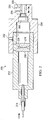
- the first and second tubes 104 and 108 may be made of fused silica, which has a relatively high level of transparency, thus allowing decoupled light to escape.
- the tubes 104 and 108 may also have substantially greater masses than the MCO 102 and VBG plate 106 for sinking any heat fluxes that are generated.
- Certain embodiments incorporating fused silica may provide an advantage in that this material has a CTE relatively similar to that of the MCO 102 and VBG plate 106 to which they are attached.
- the laser cavity inside the tubes 104 and 108 are symmetrical around the major optical axis, while joints are peripherally disposed around the major optical axis. In this manner, the physical characteristics may be maintained relatively consistent over large temperature variations.
- Lens 218 is separated from lens 216 using a spacer 226.
- the spacer 226 may be fabricated from a suitable low CTE alloy.
- the lens 218 may also be fabricated from a molded pre-form and equipped with the antireflection (AR) coating.
- Lens 218 also formats the pump light.
- the lens 218 is mounted and athermally bonded into the third tube 212.
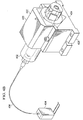
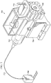
- FIGURES 3A and 3B illustrate perspective and exploded views, respectively, of an example solid-state lasing device 300 coupled to a pump diode 316 according to one embodiment of the present disclosure.
- the solid-state lasing device 300 includes a MCO 302 configured on a first tube 304, an VBG plate 306 configured on a second tube 308, and a fiber optic assembly 314 configured on a third tube 312 that may be coupled together using a telescoping (slip) fit.
- the solid-state lasing device 300 also includes several heat sink elements 318 configured on the first tube 304.
- the illustrated views show the component's axial and radial assembly arrangement resulting in a relatively compact laser.
- the overall package size as shown is approximately 1.0 inch diameter by 3.0 inches in length and weighs less than 2 ounces. Other embodiments may have dimensional sizes and weights that differ from those described herein.
- the heat sink elements 318 in this particular embodiment comprise thermo-electric coolers (TECs) also commonly known as Peltier devices that absorbs heat or thermal energy generated by the MCO 302. Efficient commercial thermal plate spreaders are also applicable due to the relatively small heat flux magnitudes. Additionally, although the solid-state lasing device 300 as shown includes three TECs, other embodiments may include more than three or less than three TECs.
- the heat sink elements 318 are symmetrically positioned on the outer surface of glass tubular unit and are positioned on the first tube 302 to provide a relatively short heat conduction path to the MCO 302.
- the heat sink elements 318 are affixed to flattened surfaces around the periphery of the first tube 302.
- the spool 610 provides a mounting structure for and forms a heat sink for the light generating devices 604.
- the spool 610 is fabricated from a heat conductive alloy with embedded V-groove features for precision positioning of the optical fiber cables 606 and mounting/guiding segments.
- the spool's large thermal mass relative to the small mass of fiber makes it an efficient thermal spreader for heat generated in the curved fiber.
- FIGURE 7 illustrates another example optical assembly 700 according to one embodiment of the present disclosure.
- the optical assembly includes a miniaturized solid-state lasing device 702 configured in a metal block 704, thermally coupled to a passive heat sink 706, and optically coupled to a light generating device 708 through a section of optical fiber 710.
- the optical assembly 700 also includes a passive Q-switch bleaching light generating device 712 that injects a pump light beam into the MCO Q-switch layer to optically bleach the laser cavity in the solid-state lasing device for pulse repetition frequency setting and precise pulse timing control.
- the bleach light generating device 712 is mounted to an integral heat sink for thermal management in the above described manner.
- the mounting structures may include one or more additional elements for thermal coupling to the heat sink elements configured on the solid-state lasing device 402. Additionally, the mounting structure may also include mounting features, such as rubber grommets that reduce physical shock and vibration energy from being conveyed from a housing on which the mounting structure is mounted to the solid-state lasing device 402.
Landscapes
- Physics & Mathematics (AREA)
- Electromagnetism (AREA)
- Engineering & Computer Science (AREA)
- Plasma & Fusion (AREA)
- Optics & Photonics (AREA)
- Lasers (AREA)
- Optical Couplings Of Light Guides (AREA)
Applications Claiming Priority (2)
| Application Number | Priority Date | Filing Date | Title |
|---|---|---|---|
| US13/417,097 US9001862B2 (en) | 2012-03-09 | 2012-03-09 | Miniaturized solid-state lasing device, system and method |
| PCT/US2013/021028 WO2013133909A1 (en) | 2012-03-09 | 2013-01-10 | Miniaturized solid-state lasing device, system, and method |
Publications (3)
| Publication Number | Publication Date |
|---|---|
| EP2823538A1 EP2823538A1 (en) | 2015-01-14 |
| EP2823538A4 EP2823538A4 (en) | 2015-12-02 |
| EP2823538B1 true EP2823538B1 (en) | 2020-05-13 |
Family
ID=49114101
Family Applications (1)
| Application Number | Title | Priority Date | Filing Date |
|---|---|---|---|
| EP13757321.8A Active EP2823538B1 (en) | 2012-03-09 | 2013-01-10 | Miniaturized solid-state lasing device and method |
Country Status (5)
| Country | Link |
|---|---|
| US (1) | US9001862B2 (2) |
| EP (1) | EP2823538B1 (2) |
| JP (1) | JP6023223B2 (2) |
| IL (1) | IL234213B (2) |
| WO (1) | WO2013133909A1 (2) |
Families Citing this family (7)
| Publication number | Priority date | Publication date | Assignee | Title |
|---|---|---|---|---|
| JP6532295B2 (ja) * | 2015-05-25 | 2019-06-19 | 株式会社メガオプト | 多波長レーザー発振装置および多波長レーザー発振方法 |
| JP2017188596A (ja) * | 2016-04-07 | 2017-10-12 | 三菱電機株式会社 | 光モジュール |
| US20200001423A1 (en) * | 2018-06-27 | 2020-01-02 | Edmund Optics, Inc. | Power polishing apparatuses and methods for in-situ finishing and coating of optical component |
| CN110423990A (zh) * | 2019-09-03 | 2019-11-08 | 肇庆宏旺金属实业有限公司 | 一种钢带镀膜系统 |
| US10907967B1 (en) | 2019-10-02 | 2021-02-02 | Honeywell International Inc. | Ring laser gyroscopes with active volume Bragg grating |
| JP2021100092A (ja) * | 2019-12-19 | 2021-07-01 | 一哲 高橋 | レーザ装置 |
| US11947048B2 (en) | 2020-05-06 | 2024-04-02 | Waymo Llc | Crosstalk reduction for light detection and ranging (lidar) devices using wavelength locking |
Citations (1)
| Publication number | Priority date | Publication date | Assignee | Title |
|---|---|---|---|---|
| US4730335A (en) * | 1986-06-26 | 1988-03-08 | Amoco Corporation | Solid state laser and method of making |
Family Cites Families (21)
| Publication number | Priority date | Publication date | Assignee | Title |
|---|---|---|---|---|
| US4665529A (en) * | 1986-05-19 | 1987-05-12 | Spectra-Physics, Inc. | Laser diode pumped solid state laser with miniaturized quick disconnect laser head |
| US4865436A (en) | 1986-03-25 | 1989-09-12 | Honeywell Inc. | Low cost ring laser angular rate sensor |
| US4723257A (en) * | 1986-05-19 | 1988-02-02 | Spectra-Physics, Inc. | Laser diode pumped solid state laser with miniaturized laser head |
| US4734912A (en) * | 1986-06-06 | 1988-03-29 | Lightwave Electronics Corp. | Laser diode end pumped Nd:YAG single mode laser |
| US4861134A (en) * | 1988-06-29 | 1989-08-29 | American Telephone And Telegraph Company, At&T Bell Laboratories | Opto-electronic and optical fiber interface arrangement |
| SE468337B (sv) * | 1991-05-08 | 1992-12-14 | Radians Innova Ab | Saett att anordna och justera in en laser samt laseranordning vilken genomfoer saettet |
| US5214444A (en) * | 1991-09-19 | 1993-05-25 | Eastman Kodak Company | Optical fiber mount and support |
| DE19723269A1 (de) * | 1997-06-03 | 1998-12-10 | Heidelberger Druckmasch Ag | Festkörperlaser mit einer oder mehreren Pumplichtquellen |
| US6055815A (en) | 1998-10-30 | 2000-05-02 | Litton Systems, Inc. | Temperature-controlled microchip laser assembly and associated submount assembly |
| JP2002182073A (ja) | 2000-12-11 | 2002-06-26 | Nippon Sheet Glass Co Ltd | 光源−光ファイバ結合器 |
| US6811916B2 (en) * | 2001-05-15 | 2004-11-02 | Neah Power Systems, Inc. | Fuel cell electrode pair assemblies and related methods |
| EP1649564A4 (en) | 2003-07-03 | 2007-09-05 | Pd Ld Inc | USE OF VOLUME BRAGG GRIDS FOR THE PREPARATION OF LASER EMISSION SCALE SIZES |
| WO2005030980A2 (en) | 2003-09-22 | 2005-04-07 | Snake Creek Lasers Llc | High densiity methods for producing diode-pumped micro lasers |
| US7590160B2 (en) | 2004-11-26 | 2009-09-15 | Manni Jeffrey G | High-gain diode-pumped laser amplifier |
| US8031749B2 (en) * | 2005-09-20 | 2011-10-04 | Jds Uniphase Corporation | Passively Q-switched microlaser with controllable peak power density |
| US20080291460A1 (en) | 2005-12-28 | 2008-11-27 | Arkady Khatchaturov | Opto-Electronic System and Method for Detecting Perturbations |
| US20090059980A1 (en) * | 2007-03-16 | 2009-03-05 | Braun Alan M | High-stability frequency reference based on self-locked alkali-vapor laser |
| KR101458077B1 (ko) | 2008-05-01 | 2014-11-04 | 삼성전자 주식회사 | 발광 소자 및 그의 제조방법 |
| WO2010138552A1 (en) | 2009-05-26 | 2010-12-02 | Redfern Integrated Optics, Inc. | Achieving low phase noise in external cavity laser implemented using planar lightwave circuit technology |
| JP2011014646A (ja) * | 2009-06-30 | 2011-01-20 | Ngk Spark Plug Co Ltd | 受動qスイッチ固体レーザ発振装置及びレーザ着火装置 |
| US8483248B2 (en) * | 2010-09-14 | 2013-07-09 | Raytheon Company | Laser crystal components joined with thermal management devices |
-
2012
- 2012-03-09 US US13/417,097 patent/US9001862B2/en active Active
-
2013
- 2013-01-10 JP JP2014560914A patent/JP6023223B2/ja active Active
- 2013-01-10 EP EP13757321.8A patent/EP2823538B1/en active Active
- 2013-01-10 WO PCT/US2013/021028 patent/WO2013133909A1/en not_active Ceased
-
2014
- 2014-08-20 IL IL234213A patent/IL234213B/en active IP Right Grant
Patent Citations (1)
| Publication number | Priority date | Publication date | Assignee | Title |
|---|---|---|---|---|
| US4730335A (en) * | 1986-06-26 | 1988-03-08 | Amoco Corporation | Solid state laser and method of making |
Also Published As
| Publication number | Publication date |
|---|---|
| EP2823538A4 (en) | 2015-12-02 |
| EP2823538A1 (en) | 2015-01-14 |
| JP6023223B2 (ja) | 2016-11-09 |
| IL234213B (en) | 2018-05-31 |
| JP2015509668A (ja) | 2015-03-30 |
| US20130235892A1 (en) | 2013-09-12 |
| US9001862B2 (en) | 2015-04-07 |
| WO2013133909A1 (en) | 2013-09-12 |
Similar Documents
| Publication | Publication Date | Title |
|---|---|---|
| EP2823538B1 (en) | Miniaturized solid-state lasing device and method | |
| US6785304B2 (en) | Waveguide device with mode control and pump light confinement and method of using same | |
| US7648290B2 (en) | Modular solid-state laser platform based on coaxial package and corresponding assembly process | |
| EP0327310A2 (en) | Solid state microlaser | |
| US5440574A (en) | Solid-state laser | |
| US6763050B2 (en) | Method for optical pumping of thin laser media at high average power | |
| WO2016080252A1 (ja) | 外部共振器型半導体レーザ | |
| CN100437167C (zh) | 外部谐振器和利用其的半导体激光模块 | |
| US20020186742A1 (en) | Single mode autocoupled resonator for telecommunications | |
| US7463667B2 (en) | Solid-state laser and multi-pass resonator | |
| CN118295086B (zh) | 具有波分复用器的光纤耦合激光源泵浦 | |
| JP2012209510A (ja) | 光ファイバレーザ光源 | |
| CN115066652B (zh) | 紫外激光装置 | |
| EP3780297B1 (en) | Solid-state lasers and assembly method therefor | |
| US9356420B1 (en) | Solid state laser with multiple cores coupled by fold optics | |
| US7161966B2 (en) | Side-pumped fiber laser | |
| CN113036586A (zh) | 一种片上集成高重频激光谐振腔器件和超短脉冲激光器 | |
| US8223813B2 (en) | Semiconductor laser pumped solid-state laser device | |
| JP2009010066A (ja) | パルスレーザ発振器 | |
| EP4007089B1 (en) | Fibre laser device | |
| JP2001044553A (ja) | ファイバスタブ型光デバイス及びそれを用いた光モジュール | |
| CN111600184A (zh) | 短腔激光器 | |
| CN121663320A (zh) | 一种基于尾纤直接泵浦的外腔半导体激光器封装结构 | |
| KR100796100B1 (ko) | 모드 제어 도파로형 레이저 장치 | |
| KR100232709B1 (ko) | 선택적 광 투과 필터를 구비한 반도체 레이저 모듈 |
Legal Events
| Date | Code | Title | Description |
|---|---|---|---|
| PUAI | Public reference made under article 153(3) epc to a published international application that has entered the european phase |
Free format text: ORIGINAL CODE: 0009012 |
|
| 17P | Request for examination filed |
Effective date: 20140822 |
|
| AK | Designated contracting states |
Kind code of ref document: A1 Designated state(s): AL AT BE BG CH CY CZ DE DK EE ES FI FR GB GR HR HU IE IS IT LI LT LU LV MC MK MT NL NO PL PT RO RS SE SI SK SM TR |
|
| AX | Request for extension of the european patent |
Extension state: BA ME |
|
| DAX | Request for extension of the european patent (deleted) | ||
| RA4 | Supplementary search report drawn up and despatched (corrected) |
Effective date: 20151030 |
|
| RIC1 | Information provided on ipc code assigned before grant |
Ipc: H01S 3/094 20060101ALN20151026BHEP Ipc: H01S 3/08 20060101ALN20151026BHEP Ipc: H01S 3/042 20060101ALN20151026BHEP Ipc: H01S 3/02 20060101ALI20151026BHEP Ipc: H01S 3/06 20060101AFI20151026BHEP Ipc: H01S 3/086 20060101ALI20151026BHEP |
|
| STAA | Information on the status of an ep patent application or granted ep patent |
Free format text: STATUS: EXAMINATION IS IN PROGRESS |
|
| 17Q | First examination report despatched |
Effective date: 20171120 |
|
| GRAP | Despatch of communication of intention to grant a patent |
Free format text: ORIGINAL CODE: EPIDOSNIGR1 |
|
| STAA | Information on the status of an ep patent application or granted ep patent |
Free format text: STATUS: GRANT OF PATENT IS INTENDED |
|
| RIC1 | Information provided on ipc code assigned before grant |
Ipc: H01S 3/04 20060101ALN20191209BHEP Ipc: H01S 3/02 20060101ALI20191209BHEP Ipc: H01S 3/042 20060101ALN20191209BHEP Ipc: H01S 3/08 20060101ALN20191209BHEP Ipc: H01S 3/086 20060101ALI20191209BHEP Ipc: H01S 3/06 20060101AFI20191209BHEP Ipc: H01S 3/094 20060101ALN20191209BHEP |
|
| INTG | Intention to grant announced |
Effective date: 20200108 |
|
| RIC1 | Information provided on ipc code assigned before grant |
Ipc: H01S 3/06 20060101AFI20191213BHEP Ipc: H01S 3/08 20060101ALN20191213BHEP Ipc: H01S 3/02 20060101ALI20191213BHEP Ipc: H01S 3/042 20060101ALN20191213BHEP Ipc: H01S 3/04 20060101ALN20191213BHEP Ipc: H01S 3/094 20060101ALN20191213BHEP Ipc: H01S 3/086 20060101ALI20191213BHEP |
|
| GRAJ | Information related to disapproval of communication of intention to grant by the applicant or resumption of examination proceedings by the epo deleted |
Free format text: ORIGINAL CODE: EPIDOSDIGR1 |
|
| STAA | Information on the status of an ep patent application or granted ep patent |
Free format text: STATUS: EXAMINATION IS IN PROGRESS |
|
| REG | Reference to a national code |
Ref country code: DE Ref legal event code: R079 Ref document number: 602013069071 Country of ref document: DE Free format text: PREVIOUS MAIN CLASS: H01S0003080000 Ipc: H01S0003060000 |
|
| INTC | Intention to grant announced (deleted) | ||
| GRAP | Despatch of communication of intention to grant a patent |
Free format text: ORIGINAL CODE: EPIDOSNIGR1 |
|
| STAA | Information on the status of an ep patent application or granted ep patent |
Free format text: STATUS: GRANT OF PATENT IS INTENDED |
|
| RIC1 | Information provided on ipc code assigned before grant |
Ipc: H01S 3/06 20060101AFI20200213BHEP Ipc: H01S 3/086 20060101ALI20200213BHEP Ipc: H01S 3/02 20060101ALI20200213BHEP Ipc: H01S 3/094 20060101ALN20200213BHEP Ipc: H01S 3/04 20060101ALN20200213BHEP Ipc: H01S 3/042 20060101ALN20200213BHEP Ipc: H01S 3/08 20060101ALN20200213BHEP |
|
| GRAS | Grant fee paid |
Free format text: ORIGINAL CODE: EPIDOSNIGR3 |
|
| INTG | Intention to grant announced |
Effective date: 20200312 |
|
| GRAA | (expected) grant |
Free format text: ORIGINAL CODE: 0009210 |
|
| STAA | Information on the status of an ep patent application or granted ep patent |
Free format text: STATUS: THE PATENT HAS BEEN GRANTED |
|
| AK | Designated contracting states |
Kind code of ref document: B1 Designated state(s): AL AT BE BG CH CY CZ DE DK EE ES FI FR GB GR HR HU IE IS IT LI LT LU LV MC MK MT NL NO PL PT RO RS SE SI SK SM TR |
|
| REG | Reference to a national code |
Ref country code: GB Ref legal event code: FG4D |
|
| REG | Reference to a national code |
Ref country code: CH Ref legal event code: EP |
|
| REG | Reference to a national code |
Ref country code: DE Ref legal event code: R096 Ref document number: 602013069071 Country of ref document: DE |
|
| REG | Reference to a national code |
Ref country code: AT Ref legal event code: REF Ref document number: 1271484 Country of ref document: AT Kind code of ref document: T Effective date: 20200615 |
|
| REG | Reference to a national code |
Ref country code: LT Ref legal event code: MG4D |
|
| REG | Reference to a national code |
Ref country code: NL Ref legal event code: MP Effective date: 20200513 |
|
| PG25 | Lapsed in a contracting state [announced via postgrant information from national office to epo] |
Ref country code: LT Free format text: LAPSE BECAUSE OF FAILURE TO SUBMIT A TRANSLATION OF THE DESCRIPTION OR TO PAY THE FEE WITHIN THE PRESCRIBED TIME-LIMIT Effective date: 20200513 Ref country code: SE Free format text: LAPSE BECAUSE OF FAILURE TO SUBMIT A TRANSLATION OF THE DESCRIPTION OR TO PAY THE FEE WITHIN THE PRESCRIBED TIME-LIMIT Effective date: 20200513 Ref country code: NO Free format text: LAPSE BECAUSE OF FAILURE TO SUBMIT A TRANSLATION OF THE DESCRIPTION OR TO PAY THE FEE WITHIN THE PRESCRIBED TIME-LIMIT Effective date: 20200813 Ref country code: FI Free format text: LAPSE BECAUSE OF FAILURE TO SUBMIT A TRANSLATION OF THE DESCRIPTION OR TO PAY THE FEE WITHIN THE PRESCRIBED TIME-LIMIT Effective date: 20200513 Ref country code: GR Free format text: LAPSE BECAUSE OF FAILURE TO SUBMIT A TRANSLATION OF THE DESCRIPTION OR TO PAY THE FEE WITHIN THE PRESCRIBED TIME-LIMIT Effective date: 20200814 Ref country code: PT Free format text: LAPSE BECAUSE OF FAILURE TO SUBMIT A TRANSLATION OF THE DESCRIPTION OR TO PAY THE FEE WITHIN THE PRESCRIBED TIME-LIMIT Effective date: 20200914 Ref country code: IS Free format text: LAPSE BECAUSE OF FAILURE TO SUBMIT A TRANSLATION OF THE DESCRIPTION OR TO PAY THE FEE WITHIN THE PRESCRIBED TIME-LIMIT Effective date: 20200913 |
|
| PG25 | Lapsed in a contracting state [announced via postgrant information from national office to epo] |
Ref country code: RS Free format text: LAPSE BECAUSE OF FAILURE TO SUBMIT A TRANSLATION OF THE DESCRIPTION OR TO PAY THE FEE WITHIN THE PRESCRIBED TIME-LIMIT Effective date: 20200513 Ref country code: LV Free format text: LAPSE BECAUSE OF FAILURE TO SUBMIT A TRANSLATION OF THE DESCRIPTION OR TO PAY THE FEE WITHIN THE PRESCRIBED TIME-LIMIT Effective date: 20200513 Ref country code: HR Free format text: LAPSE BECAUSE OF FAILURE TO SUBMIT A TRANSLATION OF THE DESCRIPTION OR TO PAY THE FEE WITHIN THE PRESCRIBED TIME-LIMIT Effective date: 20200513 Ref country code: BG Free format text: LAPSE BECAUSE OF FAILURE TO SUBMIT A TRANSLATION OF THE DESCRIPTION OR TO PAY THE FEE WITHIN THE PRESCRIBED TIME-LIMIT Effective date: 20200813 |
|
| REG | Reference to a national code |
Ref country code: AT Ref legal event code: MK05 Ref document number: 1271484 Country of ref document: AT Kind code of ref document: T Effective date: 20200513 |
|
| PG25 | Lapsed in a contracting state [announced via postgrant information from national office to epo] |
Ref country code: NL Free format text: LAPSE BECAUSE OF FAILURE TO SUBMIT A TRANSLATION OF THE DESCRIPTION OR TO PAY THE FEE WITHIN THE PRESCRIBED TIME-LIMIT Effective date: 20200513 Ref country code: AL Free format text: LAPSE BECAUSE OF FAILURE TO SUBMIT A TRANSLATION OF THE DESCRIPTION OR TO PAY THE FEE WITHIN THE PRESCRIBED TIME-LIMIT Effective date: 20200513 |
|
| PG25 | Lapsed in a contracting state [announced via postgrant information from national office to epo] |
Ref country code: RO Free format text: LAPSE BECAUSE OF FAILURE TO SUBMIT A TRANSLATION OF THE DESCRIPTION OR TO PAY THE FEE WITHIN THE PRESCRIBED TIME-LIMIT Effective date: 20200513 Ref country code: ES Free format text: LAPSE BECAUSE OF FAILURE TO SUBMIT A TRANSLATION OF THE DESCRIPTION OR TO PAY THE FEE WITHIN THE PRESCRIBED TIME-LIMIT Effective date: 20200513 Ref country code: IT Free format text: LAPSE BECAUSE OF FAILURE TO SUBMIT A TRANSLATION OF THE DESCRIPTION OR TO PAY THE FEE WITHIN THE PRESCRIBED TIME-LIMIT Effective date: 20200513 Ref country code: CZ Free format text: LAPSE BECAUSE OF FAILURE TO SUBMIT A TRANSLATION OF THE DESCRIPTION OR TO PAY THE FEE WITHIN THE PRESCRIBED TIME-LIMIT Effective date: 20200513 Ref country code: SM Free format text: LAPSE BECAUSE OF FAILURE TO SUBMIT A TRANSLATION OF THE DESCRIPTION OR TO PAY THE FEE WITHIN THE PRESCRIBED TIME-LIMIT Effective date: 20200513 Ref country code: EE Free format text: LAPSE BECAUSE OF FAILURE TO SUBMIT A TRANSLATION OF THE DESCRIPTION OR TO PAY THE FEE WITHIN THE PRESCRIBED TIME-LIMIT Effective date: 20200513 Ref country code: AT Free format text: LAPSE BECAUSE OF FAILURE TO SUBMIT A TRANSLATION OF THE DESCRIPTION OR TO PAY THE FEE WITHIN THE PRESCRIBED TIME-LIMIT Effective date: 20200513 Ref country code: DK Free format text: LAPSE BECAUSE OF FAILURE TO SUBMIT A TRANSLATION OF THE DESCRIPTION OR TO PAY THE FEE WITHIN THE PRESCRIBED TIME-LIMIT Effective date: 20200513 |
|
| REG | Reference to a national code |
Ref country code: DE Ref legal event code: R097 Ref document number: 602013069071 Country of ref document: DE |
|
| PG25 | Lapsed in a contracting state [announced via postgrant information from national office to epo] |
Ref country code: SK Free format text: LAPSE BECAUSE OF FAILURE TO SUBMIT A TRANSLATION OF THE DESCRIPTION OR TO PAY THE FEE WITHIN THE PRESCRIBED TIME-LIMIT Effective date: 20200513 Ref country code: PL Free format text: LAPSE BECAUSE OF FAILURE TO SUBMIT A TRANSLATION OF THE DESCRIPTION OR TO PAY THE FEE WITHIN THE PRESCRIBED TIME-LIMIT Effective date: 20200513 |
|
| PLBE | No opposition filed within time limit |
Free format text: ORIGINAL CODE: 0009261 |
|
| STAA | Information on the status of an ep patent application or granted ep patent |
Free format text: STATUS: NO OPPOSITION FILED WITHIN TIME LIMIT |
|
| 26N | No opposition filed |
Effective date: 20210216 |
|
| PG25 | Lapsed in a contracting state [announced via postgrant information from national office to epo] |
Ref country code: SI Free format text: LAPSE BECAUSE OF FAILURE TO SUBMIT A TRANSLATION OF THE DESCRIPTION OR TO PAY THE FEE WITHIN THE PRESCRIBED TIME-LIMIT Effective date: 20200513 |
|
| PG25 | Lapsed in a contracting state [announced via postgrant information from national office to epo] |
Ref country code: MC Free format text: LAPSE BECAUSE OF FAILURE TO SUBMIT A TRANSLATION OF THE DESCRIPTION OR TO PAY THE FEE WITHIN THE PRESCRIBED TIME-LIMIT Effective date: 20200513 |
|
| REG | Reference to a national code |
Ref country code: CH Ref legal event code: PL |
|
| PG25 | Lapsed in a contracting state [announced via postgrant information from national office to epo] |
Ref country code: LU Free format text: LAPSE BECAUSE OF NON-PAYMENT OF DUE FEES Effective date: 20210110 |
|
| REG | Reference to a national code |
Ref country code: BE Ref legal event code: MM Effective date: 20210131 |
|
| PG25 | Lapsed in a contracting state [announced via postgrant information from national office to epo] |
Ref country code: LI Free format text: LAPSE BECAUSE OF NON-PAYMENT OF DUE FEES Effective date: 20210131 Ref country code: CH Free format text: LAPSE BECAUSE OF NON-PAYMENT OF DUE FEES Effective date: 20210131 |
|
| PG25 | Lapsed in a contracting state [announced via postgrant information from national office to epo] |
Ref country code: IE Free format text: LAPSE BECAUSE OF NON-PAYMENT OF DUE FEES Effective date: 20210110 |
|
| PG25 | Lapsed in a contracting state [announced via postgrant information from national office to epo] |
Ref country code: BE Free format text: LAPSE BECAUSE OF NON-PAYMENT OF DUE FEES Effective date: 20210131 |
|
| PG25 | Lapsed in a contracting state [announced via postgrant information from national office to epo] |
Ref country code: HU Free format text: LAPSE BECAUSE OF FAILURE TO SUBMIT A TRANSLATION OF THE DESCRIPTION OR TO PAY THE FEE WITHIN THE PRESCRIBED TIME-LIMIT; INVALID AB INITIO Effective date: 20130110 |
|
| PG25 | Lapsed in a contracting state [announced via postgrant information from national office to epo] |
Ref country code: CY Free format text: LAPSE BECAUSE OF FAILURE TO SUBMIT A TRANSLATION OF THE DESCRIPTION OR TO PAY THE FEE WITHIN THE PRESCRIBED TIME-LIMIT Effective date: 20200513 |
|
| P01 | Opt-out of the competence of the unified patent court (upc) registered |
Effective date: 20230530 |
|
| PG25 | Lapsed in a contracting state [announced via postgrant information from national office to epo] |
Ref country code: MK Free format text: LAPSE BECAUSE OF FAILURE TO SUBMIT A TRANSLATION OF THE DESCRIPTION OR TO PAY THE FEE WITHIN THE PRESCRIBED TIME-LIMIT Effective date: 20200513 |
|
| PG25 | Lapsed in a contracting state [announced via postgrant information from national office to epo] |
Ref country code: MT Free format text: LAPSE BECAUSE OF FAILURE TO SUBMIT A TRANSLATION OF THE DESCRIPTION OR TO PAY THE FEE WITHIN THE PRESCRIBED TIME-LIMIT Effective date: 20200513 |
|
| PG25 | Lapsed in a contracting state [announced via postgrant information from national office to epo] |
Ref country code: TR Free format text: LAPSE BECAUSE OF FAILURE TO SUBMIT A TRANSLATION OF THE DESCRIPTION OR TO PAY THE FEE WITHIN THE PRESCRIBED TIME-LIMIT Effective date: 20200513 |
|
| PGFP | Annual fee paid to national office [announced via postgrant information from national office to epo] |
Ref country code: GB Payment date: 20251220 Year of fee payment: 14 |
|
| PGFP | Annual fee paid to national office [announced via postgrant information from national office to epo] |
Ref country code: FR Payment date: 20251217 Year of fee payment: 14 |
|
| PGFP | Annual fee paid to national office [announced via postgrant information from national office to epo] |
Ref country code: DE Payment date: 20251217 Year of fee payment: 14 |