EP2824445A1 - Mikroskop mit geladenen Teilchen und Raman-Spektroskopiefähigkeit - Google Patents
Mikroskop mit geladenen Teilchen und Raman-Spektroskopiefähigkeit Download PDFInfo
- Publication number
- EP2824445A1 EP2824445A1 EP13180398.3A EP13180398A EP2824445A1 EP 2824445 A1 EP2824445 A1 EP 2824445A1 EP 13180398 A EP13180398 A EP 13180398A EP 2824445 A1 EP2824445 A1 EP 2824445A1
- Authority
- EP
- European Patent Office
- Prior art keywords
- feature
- sample
- raman
- charged
- microscope
- Prior art date
- Legal status (The legal status is an assumption and is not a legal conclusion. Google has not performed a legal analysis and makes no representation as to the accuracy of the status listed.)
- Granted
Links
Images


Classifications
-
- H—ELECTRICITY
- H01—ELECTRIC ELEMENTS
- H01J—ELECTRIC DISCHARGE TUBES OR DISCHARGE LAMPS
- H01J37/00—Discharge tubes with provision for introducing objects or material to be exposed to the discharge, e.g. for the purpose of examination or processing thereof
- H01J37/26—Electron or ion microscopes; Electron or ion diffraction tubes
- H01J37/261—Details
-
- G—PHYSICS
- G01—MEASURING; TESTING
- G01N—INVESTIGATING OR ANALYSING MATERIALS BY DETERMINING THEIR CHEMICAL OR PHYSICAL PROPERTIES
- G01N21/00—Investigating or analysing materials by the use of optical means, i.e. using sub-millimetre waves, infrared, visible or ultraviolet light
- G01N21/62—Systems in which the material investigated is excited whereby it emits light or causes a change in wavelength of the incident light
- G01N21/63—Systems in which the material investigated is excited whereby it emits light or causes a change in wavelength of the incident light optically excited
- G01N21/65—Raman scattering
-
- H—ELECTRICITY
- H01—ELECTRIC ELEMENTS
- H01J—ELECTRIC DISCHARGE TUBES OR DISCHARGE LAMPS
- H01J37/00—Discharge tubes with provision for introducing objects or material to be exposed to the discharge, e.g. for the purpose of examination or processing thereof
- H01J37/02—Details
- H01J37/22—Optical, image processing or photographic arrangements associated with the tube
- H01J37/226—Optical arrangements for illuminating the object; optical arrangements for collecting light from the object
-
- H—ELECTRICITY
- H01—ELECTRIC ELEMENTS
- H01J—ELECTRIC DISCHARGE TUBES OR DISCHARGE LAMPS
- H01J37/00—Discharge tubes with provision for introducing objects or material to be exposed to the discharge, e.g. for the purpose of examination or processing thereof
- H01J37/26—Electron or ion microscopes; Electron or ion diffraction tubes
- H01J37/28—Electron or ion microscopes; Electron or ion diffraction tubes with scanning beams
-
- H—ELECTRICITY
- H01—ELECTRIC ELEMENTS
- H01J—ELECTRIC DISCHARGE TUBES OR DISCHARGE LAMPS
- H01J2237/00—Discharge tubes exposing object to beam, e.g. for analysis treatment, etching, imaging
- H01J2237/30—Electron or ion beam tubes for processing objects
- H01J2237/317—Processing objects on a microscale
- H01J2237/3174—Etching microareas
- H01J2237/31745—Etching microareas for preparing specimen to be viewed in microscopes or analyzed in microanalysers
Definitions
- the invention relates to a method of examining a sample using a combined charged-particle microscope and Raman spectroscope, whereby:
- the invention also relates to a charged-particle microscope in which such a method can be performed.
- Electron microscopy is a well-known technique for imaging microscopic objects.
- the basic genus of electron microscope has undergone evolution into a number of well-known apparatus species, such as the Transmission Electron Microscope (TEM), Scanning Electron Microscope (SEM), and Scanning Transmission Electron Microscope (STEM).
- TEM Transmission Electron Microscope
- SEM Scanning Electron Microscope
- STEM Scanning Transmission Electron Microscope
- STEM Scanning Transmission Electron Microscope
- a beam of particulate radiation such as an electron beam or ion beam
- emitted radiation may, for example, comprise Secondary Electrons, Backscatter (BS) Electrons, visible/infrared/ultraviolet light (cathodoluminescence) and X-rays.
- BS Secondary Electrons
- Cathodoluminescence visible/infrared/ultraviolet light
- X-rays X-rays.
- electrons are relatively easy and cheap to detect, e.g. using a (solid-state or evacuated) photo-multiplier tube (PMT) in conjunction with a scintillator.
- PMT photo-multiplier tube
- X-ray detectors generally tend to be relatively expensive and slow, but they are useful in performing compositional/elemental analyses of samples, such as in the case of so-called EDX (Energy Dispersive X-ray Spectroscopy) detectors, for example.
- EDX Electron Energy-Loss Spectroscopy
- spectroscopic techniques such as EDX and EELS
- EDX and EELS have been traditionally available in CPMs
- a far more useful/versatile spectroscopic technique is Raman spectroscopy, which probes a sample using a focused beam of optical radiation (light) rather than a charged-particle beam.
- Raman spectroscopy is relatively fast and accurate, and can provide very detailed information on parameters such as molecular composition, chirality, polymer chain length, crystalline structure, bond formation, etc .
- CPM analysis can yield information regarding (mineral/crystal) grain size, shape and location
- RS analysis can yield information concerning chemical composition/concentration and crystalline structure, allowing much more information to be extracted from (possibly precious/rare/costly/fragile) sample material.
- CPM and RS analysis complement each other in terms of the nature of the information that they provide, they also suffer from a substantial incompatibility. This has to do with the fact that both techniques use a different type of probing beam (charged particles vs . photons), with very different attainable lateral resolutions (of the order of nanometers vs . microns). This is not such a problem in fields such as mineralogy/petrology or the semiconductor industry, where structures being investigated (mineral/crystal grains or semiconductor devices, for example) are typically relative large - i.e. larger than the minimum attainable lateral resolution of either a CPM or RS.
- Radar signal is here intended to refer to a detector signal produced by light that undergoes inelastic/Raman scattering at the sample in question; such a signal may comprise one or more Raman spectral lines.
- Raman spectral lines To qualify such a signal as “expected” is merely to label it as being a future occurrence, i.e. as being a signal that has yet to be obtained; the term “expected” does not necessarily imply that one has any prior knowledge/forecast of what said signal will look like.
- the surface modification technique is enacted upon the surface of the sample that "faces” the incoming charged-particle beam in the CPM, and that is to face the incoming optical beam of the RS.
- positive discrimination indicates relative enhancement, e.g. by strengthening and/or making more identifiable and/or filtering out unwanted "ancillary" signals, for instance.
- the inventive approach seeks to cause positive discrimination of the (expected) Raman signal from a feature of interest relative to the (expected) Raman signal from the essentially uninteresting/irrelevant "landscape” surrounding/adjoining that feature.
- Such discrimination can be achieved via appropriate use of an in situ surface modification technique (SMT), as will be elucidated in more detail below.
- SMT in situ surface modification technique
- said SMT is selected from the group comprising Electron Beam-Induced Deposition (EBID), Ion Beam-Induced Deposition (IBID), Electron Beam-Induced Etching (EBIE), Ion Beam-Induced Etching (IBIE), Focused Ion Beam (FIB) milling, and combinations hereof.
- EBID Electron Beam-Induced Deposition
- IBID Ion Beam-Induced Deposition
- EBIE Electron Beam-Induced Etching
- IBIE Ion Beam-Induced Etching
- FIB Focused Ion Beam
- the abovementioned positive discrimination is achieved by depositing a blanketing material on at least part of said portion other than said feature ( i.e. on at least a part of said "landscape"), whereby said blanketing material is chosen so as to exhibit an effect selected from the group comprising:
- Such a blanketing layer will produce a known/reference Raman signal that differs from the Raman signal from said feature; suitable manipulation of the obtained spectrum (e.g. a subtraction/filtering operation) allows the spectrum of said feature to be derived from the combined Raman signal.
- suitable manipulation of the obtained spectrum e.g. a subtraction/filtering operation
- the aforementioned positive discrimination is caused by depositing an enhancing structure proximal said feature, which structure serves to amplify a Raman signal from said feature.
- an enhancing structure proximal said feature, which structure serves to amplify a Raman signal from said feature.
- Such a structure may take different forms, such as set forth in the following examples:
- the invention can also be performed using a subtractive SMT; in such an instance, the aforementioned positive discrimination is caused by removing material from said portion other than said feature (i.e. from at least part of said "landscape").
- FIB milling or EBIE/IBIE
- EBIE/IBIE can be used to accurately remove material from around the feature of interest, so that the feature remains behind on a "pillar" that is surrounded by a "pit” in the sample surface.
- the depth of this pit is such that its bottom is essentially outside the focal reach of the probing RS beam, and its width is preferably as large as (or larger than) the diameter D of the RS field of view / light spot.
- the depth of such a pit may be of the order of about 2-3 ⁇ m, for instance (a depth that can typically be achieved in a matter of minutes using a technique such as FIB milling).
- the SMT used to produce a pit as alluded to in the previous paragraph also causes inclusion/implantation of certain atomic/molecular species in the bottom of said pit.
- certain atomic/molecular species for example, FIB milling performed using Ga ions can leave a layer of Ga dopant in the pit bottom. In this way, even if the pit is not deep enough to fall outside the focal reach of the probing RS beam, its bottom will produce a Raman spectrum with an identifiable Ga signature, which can be subtracted from the total Raman spectrum to reveal the spectrum of the feature of interest.
- the current invention provides a way in which to effectively improve the attainable resolution of Raman spectroscopy when performed on a sample that has been previously investigated using a CPM, whereby clever SMTs are used to allow an RS to "zoom in” on features that are well within the resolution capability of the CPM but below the nominal resolution capability of the RS.
- an embodiment of the current invention provides a sample under investigation with an alignment mark that can be detected by both the employed CPM and the RS.
- Such a mark should preferably have the following attributes:
- the alignment mark in question can be provided using an SMT such as EBID/IBID, for example.
- SMT such as EBID/IBID
- FIB milling for example, whereby Ga ions (for instance) implanted in the sample by the FIB provide a chemical signature that can be recognized in the RS.
- the alignment mark is preferably relatively small, so as to maximize alignment accuracy, but it must be large enough to be satisfactorily detectable in the RS. Since the strength of a Raman signal will depend on the amount of material generating it, a mark that has relatively small lateral dimensions can still generate an acceptable Raman signal if it has a relatively large thickness (by way of compensation for its relatively small lateral area).
- the alignment mark is approximately the size of the field of view of the RS. It may, for example, have the shape of a cross or grating.
- a combined CPM/RS can be provided with an optical position measuring system (comprising interferometers and/or encoders, for example) that allows the positional coordinates of a substrate holder (on which the substrate is mounted) to be determined relative to a (fixed) reference point ( e.g. on a metrology frame).
- an optical position measuring system comprising interferometers and/or encoders, for example
- a substrate holder on which the substrate is mounted
- a (fixed) reference point e.g. on a metrology frame
- a "capture scan” can be performed at the new station so as to locate said alignment mark; once this is located, said feature can be automatically located using the coordinates referred to above.
- An alignment / position measuring system of this type allows potential positioning errors - such as shift, skew and rotation errors - to be mitigated.
- an optical position measuring system one could also conceive a position measuring system based on other principles, such as capacitance measurement, for example; the skilled artisan will be familiar with such possible alternatives.
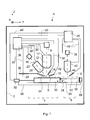
- FIG. 1 is a highly schematic depiction of an embodiment of an apparatus A according to the current invention, in which an embodiment of a method according to the current invention can be enacted.
- a charged-particle microscope (CPM) 4 and a Raman spectroscope (RS) 6 are both located in a shared vacuum enclosure 2, the RS 6 being disposed "off-axis" with respect to the CPM 4 (see below).
- the depicted CPM 4 is a so-called “FIB-SEM", as will be elucidated in more detail in what follows; however, this does not necessarily have to be the case, and the employed CPM 4 might instead comprise a TEM, for example.
- the employed RS 6 could, in principle, be arranged so as to be "on-axis" with respect to the CPM 4. The skilled artisan will understand the various choices that can be made in these regards.
- an electron source 8 (such as a Schottky gun, for example) produces a beam of electrons that traverse a particle-optical column 10 that serves to focus them onto a chosen region of a substrate S.
- This particle-optical column 10 has a particle-optical axis 12, and will generally comprise a variety of electrostatic / magnetic lenses, deflectors, correctors (such as stigmators), etc .
- This focused electron beam will interact with the sample S in such a manner as to cause various types of "stimulated" radiation to be emitted from the sample S - including (for example) secondary electrons, backscattered electrons, X-rays and optical radiation (cathodoluminescence) - and one or more of these radiation types can be detected with the aid of detectors 14, 16.
- detector 14 might be a combined scintillator/PMT
- detector 16 might be an EDX detector, for instance.
- the CPM 4 depicted here also has an ion-based functionality.
- an ion gun 18 produces a beam of ions (e.g. Ga ions) that traverse a particle-optical column 20 that serves to focus them onto the substrate S (within the field of view of the electron particle-optical column 10).
- This ion particle-optical column 20 has a particle-optical axis 22.
- the ion particle-optical column 20 can be used to perform ion-based imaging of the sample S (with the aid of detectors 14, 16, for example) and/or it can be used to perform ion-based surface modification techniques (SMTs) on the sample S, as will be explained below.
- SMTs surface modification techniques
- a gas administration nozzle 24 that is connected to a gas supply conduit 26 containing a valve/regulator 28; with the aid of these features 24, 26, 28 a suitable gas-phase precursor substance can be administered in a controlled manner to the vicinity of the point of intersection of the optical axes 12, 22, where it can interact with an electron beam travelling along axis 12 (to perform EBID/EBIE) and/or an ion beam travelling along axis 22 (to perform IBIB/IBIE) so as to cause highly localized deposition/etching at the exposed surface of the substrate S (depending on the type of precursor substance administered).
- EBID/EBIE electron beam travelling along axis 12
- IBIB/IBIE ion beam travelling along axis 22
- an ion beam travelling along axis 22 can be used to perform localized FIB milling of (and ion implantation in) the exposed surface of the substrate S, in which case a precursor substance does not necessarily have to be administered from nozzle 24.
- the substrate S is held on a substrate holder 30 than can be positioned in multiple degrees of freedom by a positioning device (stage) 32.
- the substrate holder 30 may comprise a chuck that can be moved smoothly in the XY plane (see the depicted Cartesian coordinate system), e.g. by sliding it over a flat reference surface 34 with the aid of an interposed bearing.
- Such movement allows different regions of the substrate S to be imaged and/or subjected to an SMT within the CPM 4.
- it also allows the substrate S to be moved to a location where it can be analyzed using the RS 6, as will be elucidated in more detail below.
- the CPM 4 is controlled by a controller (computer processor) 36, which is connected to various components of the CPM 4 via control lines (buses) 36'.
- This controller 36 can provide a variety of functions, such as synchronizing actions, providing setpoints, processing signals, performing calculations and displaying messages/information on a display device (not depicted), such as a flat panel display, for example.
- the apparatus A includes an RS 6.
- This comprises a light source (e.g. laser) 38 that can be used to produce (non-ionizing) monochromatic light, e.g. with a wavelength ⁇ of 514 nm or 785 nm, for instance.
- This light traverses an optical column 40 that serves to focus light from the source 38 onto a focal plane that is matched to the Z position of the substrate S (indicated here by dashed line S').
- This optical column 40 has an optical axis 42, and will generally comprise a variety of lenses/mirrors, and possibly also other optical components, such as filters, polarizers, aperture plates, etc .
- Light focused by the optical column 40 will produce a light spot of diameter D on the exposed surface of the substrate S (see Figure 2 , for example), and light in this spot will undergo inelastic (Raman) scattering by irradiated molecules in the substrate S; as a result, the scattered light will contain (slightly shifted) wavelengths other than ⁇ .
- the spectroscopic optical detector 44 can be used to collect (a portion of) this scattered light, and produce a Raman spectrum for the irradiated portion of the substrate S.
- the RS 6 is controlled by a controller (computer processor) 46, which is connected to various components of the RS 6 via control lines (buses) 46'.
- This controller 46 can provide a variety of functions, such as synchronizing actions, providing setpoints, processing signals, performing calculations and displaying messages/information on a display device (not depicted), such as a flat panel display, for example.
- the controller 46 is also connected to the controller 36 via a control line (bus) 50.
- the RS 6 does not necessarily have to be located in a vacuum environment in order to function properly. Accordingly, if one so desired, the RS 6 could be located outside the vacuum enclosure 2, and an airlock system (not depicted) could be used to allow the substrate holder 30 to shuttle back and forth between the CPM 4 and the RS 6. Alternatively, a transparent window could be located in the wall of the vacuum enclosure 2, so as to allow the RS 6 to optically access the inside of the vacuum enclosure 2. All such variants are examples of a "combined CPM and RS" as alluded to in the context of the current invention.
- the RS 6 is disposed "off-axis" with respect to the CPM 4, in that the optical axis 42 of the RS 6 and the particle-optical axes 12, 22 of the CPM 4 do not have a common point of intersection.
- This particular configuration is chosen in this case so as to prevent excessive cluttering of the space around the sample S in the CPM 4; however, this does not necessarily have to be the case, and one could instead choose an "on-axis" configuration, whereby the CPM 4 and RS 6 both "look at" ( i.e. are aligned toward) a common point.
- a position measuring system with which the position of the substrate holder 30 can be measured.
- This PMS comprises a (laser) light source 60 that produces a (collimated) light beam 62 that is directed at the substrate holder 30.
- a reflective element 64 e.g. interferometer retroflector or reflective encoder scale
- the detector 66 can determine the (momentary) position of the substrate holder 30, and share this information (in a feedback loop) with the positioning device 32 via control line (bus) 68.
- Items 62,64,66,68 collectively form a measurement "branch", which serves to measure position along a single direction/axis (e.g. Y position if branch 60,62,64,66 is interferometry-based, or X position if it is encoder-based). Although only one such branch is depicted here, a typical PMS will contain a plurality of such branches along complementary axes, so as to be able to measure position in plural coordinates (e.g. Y and X).
- the CPM 4 and RS 6 will each have an alignment functionality, by means of which they can locate an alignment mark on the substrate S (and also possibly on the substrate holder 30).
- This alignment functionality works together with the PMS described in the previous paragraph to allow the position of features on the substrate S to be determined relative to a reference that can be used by both the CPM 4 and the RS 6.
- the skilled artisan will be very familiar with the structure and operation of such alignment systems, which need not be discussed here in greater detail.
- the substrate S may be provided on its topside with an alignment mark (not depicted) that can be imaged (“seen”) by CPM 4 and that can be chemically detected (“sniffed out”) by RS 6 - thus allowing such a mark to be jointly utilized by both the CPM 4 and the RS 6.
- an alignment mark (not depicted) that can be imaged (“seen”) by CPM 4 and that can be chemically detected (“sniffed out”) by RS 6 - thus allowing such a mark to be jointly utilized by both the CPM 4 and the RS 6.
- the interior of the enclosure 2 does not have to be kept at a strict vacuum; for example, in a so-called “Environmental SEM", a background atmosphere of a given gas is deliberately introduced/maintained within the enclosure 2.
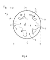
- Figure 2 renders a plan view of an aspect of part of the apparatus A of Figure 1 when in use, more particularly a (schematic) field of view V of the RS 6 of Figure 1 .
- the field of view V is a circle of diameter D.
- a portion P of the sample S is visible, comprising various features 1 that can be identified against a "background" 3. For example:
- some of the features 1 have lateral dimensions (in the XY plane) that are (much) smaller than D.
- D is of the order of about 1 ⁇ m and the features 1 have (exemplary) lateral dimensions ranging from about 20 nm to about 200 nm.
- Such feature sizes can be easily resolved using the CPM 4 of Figure 1 and, in a prior investigation of the sample S using that CPM 4, a particular feature F amongst the features 1 has been identified as being of interest.
- the CPM 4 can provide good information regarding the shape/geometry of feature F, and also some information regarding its composition ( via EDX, for example), more detailed compositional information regarding the feature F is desired, e.g. via a Raman spectrum obtained using the RS 6.
- the current invention addresses this problem by using in situ SMTs to prepare the sample S after investigation by the CPM 4 and prior to analysis by the RS 6, in such a manner as to cause positive discrimination of an expected Raman signal from feature F relative to an expected Raman signal from the rest of the field of view V excluding F, i.e. from the "landscape" L surrounding F (in the current example, this landscape L comprises the background 3 and all features 1 other than F). Examples of the inventive method using different SMTs will now be given.
- a "mask" 5 of blanketing material (such as Au, Al or Ag) has been deposited on the sample S so as to cover the landscape L in the field of view V with the exception of a small exclusion zone 7 around the feature F.
- the exclusion zone 7 is schematically depicted as being a relatively "roomy” circle around the feature F but, if so desired, it may take other shapes, and, in particular, may be more tightly fitted/matched to the outline of feature F.
- the mask 5 can be deposited using a technique such as EBID or IBID at the CPM 4 in Figure 1 , for instance (as set forth above).
- a Raman spectrum of the field of view V in this case will be the sum of:
- the spectrum (ii) may be:
- the effect of using the mask 5 is essentially to "replace" the unknown landscape L by a controlled neighborhood 5, thus effectively narrowing the resolution of the RS 6 down to the size of the exclusion zone 7.
- the enhancing structure E alluded to above takes the form of a localized "patch” 9 comprising a non-continuous layer 11 of (metallic) material, which patch 9 is disposed on top of the feature F ( i.e. so as to overlie it along the Z direction).
- non-continuous here refers to a layer that is not fully “closed”, but instead comprises distributed openings, e.g. as in the case of a grid structure.
- An example of such a grid is an array of metallic (e.g. Au, Ag or Al) nano-dots of size ca.
- the patch 9 is schematically depicted as being a relatively "roomy" ellipse around the feature F but, if so desired, it may take other shapes, and, in particular, may be more tightly fitted/matched to the outline of feature F (so as to overlay less of the background 3).
- such a structure E can serve to significantly amplify the Raman signal from feature F (and any piece of the background 3 underneath the patch 9), e.g. by a factor of as much as 100-10,000.
- the Raman spectrum from feature F is augmented to such an extent that it effectively "drowns out” the (unknown) Raman spectrum from landscape L.
- This embodiment effectively represents a form of localized Surface-Enhanced Raman Spectroscopy (SERS), whereby pertinent surface enhancement is confined to the feature of interest (and its immediate vicinity).
- SERS Surface-Enhanced Raman Spectroscopy
- FIG. 5 depicts an alternative enhancing structure E, which now takes the form of a so-called "bow-tie" antenna B, having two (substantially triangular) segments/wings B1, B2 that are symmetrically positioned so as to straddle feature F.
- the bow-tie B acts as a nano-antenna that substantially amplifies the Raman spectrum from feature F via plasmonic resonance effects.
- the bow-tie B is aligned along the Y direction, but this does not necessarily have to be the case, and it can also have other orientations in the XY plane.
- the segments/wings B1, B2 are comprised of a metal such as Au, for example, and were deposited at the desired/required location with respect to feature F using the EBID and/or IBID functionality at CPM 4 in Figure 1 , for instance.
Landscapes
- Chemical & Material Sciences (AREA)
- Analytical Chemistry (AREA)
- Health & Medical Sciences (AREA)
- Nuclear Medicine, Radiotherapy & Molecular Imaging (AREA)
- Physics & Mathematics (AREA)
- Life Sciences & Earth Sciences (AREA)
- Biochemistry (AREA)
- General Health & Medical Sciences (AREA)
- General Physics & Mathematics (AREA)
- Immunology (AREA)
- Pathology (AREA)
- Investigating, Analyzing Materials By Fluorescence Or Luminescence (AREA)
Priority Applications (2)
| Application Number | Priority Date | Filing Date | Title |
|---|---|---|---|
| JP2014135604A JP6116529B2 (ja) | 2013-07-08 | 2014-07-01 | ラマン分光機能を有する荷電粒子顕微鏡 |
| CN201410321370.5A CN104280377B (zh) | 2013-07-08 | 2014-07-08 | 具有拉曼光谱能力的带电粒子显微镜 |
Applications Claiming Priority (1)
| Application Number | Priority Date | Filing Date | Title |
|---|---|---|---|
| US201361843747P | 2013-07-08 | 2013-07-08 |
Publications (2)
| Publication Number | Publication Date |
|---|---|
| EP2824445A1 true EP2824445A1 (de) | 2015-01-14 |
| EP2824445B1 EP2824445B1 (de) | 2016-03-02 |
Family
ID=48951411
Family Applications (1)
| Application Number | Title | Priority Date | Filing Date |
|---|---|---|---|
| EP13180398.3A Active EP2824445B1 (de) | 2013-07-08 | 2013-08-14 | Mikroskopie mit geladenen teilchen kombiniert mit raman-spektroskopie |
Country Status (4)
| Country | Link |
|---|---|
| US (1) | US9406482B2 (de) |
| EP (1) | EP2824445B1 (de) |
| JP (1) | JP6116529B2 (de) |
| CN (1) | CN104280377B (de) |
Cited By (1)
| Publication number | Priority date | Publication date | Assignee | Title |
|---|---|---|---|---|
| EP3104392A1 (de) | 2015-06-09 | 2016-12-14 | FEI Company | Verfahren zur analyse von oberflächenmodifikationen einer probe in eines ladungsträger-mikroskop |
Families Citing this family (13)
| Publication number | Priority date | Publication date | Assignee | Title |
|---|---|---|---|---|
| EP2993682A1 (de) | 2014-09-04 | 2016-03-09 | Fei Company | Verfahren zur Spektroskopiedurchführung in einem Transmissions-Ladungsträger-Mikroskop |
| EP2998979A1 (de) | 2014-09-22 | 2016-03-23 | Fei Company | Verbesserte Spektroskopie in einem Transmissionsmikroskop mit geladenen Partikeln |
| JP6622061B2 (ja) * | 2015-11-04 | 2019-12-18 | 日本電子株式会社 | 荷電粒子線装置 |
| EP3345119A4 (de) | 2016-01-29 | 2019-04-24 | Hewlett-Packard Development Company, L.P. | Optische leser |
| EP3231682B1 (de) * | 2016-04-15 | 2018-12-26 | Volvo Car Corporation | Übernahmeaufforderungsanordnung, fahrzeug und verfahren zur bereitstellung einer übernahmeaufforderung |
| JP6831190B2 (ja) * | 2016-08-15 | 2021-02-17 | トヨタ自動車株式会社 | 自動運転車両の制御システム及び制御方法 |
| JP6814109B2 (ja) * | 2017-08-25 | 2021-01-13 | 株式会社日立製作所 | 微細構造体の加工方法、および微細構造体の加工装置 |
| JP7017437B2 (ja) * | 2018-03-06 | 2022-02-08 | Tasmit株式会社 | 反射電子のエネルギースペクトルを測定する装置および方法 |
| CN110044875B (zh) * | 2019-04-26 | 2024-04-19 | 南京信息工程大学 | 一种用于激光诱导击穿光谱技术的气溶胶检测瞄准装置 |
| US11994472B2 (en) * | 2019-07-26 | 2024-05-28 | The Board Of Trustees Of The Leland Stanford Junior University | Sub-wavelength Raman imaging with combined optical and electron excitation |
| KR102739071B1 (ko) * | 2019-08-05 | 2024-12-06 | 삼성전자주식회사 | 미세먼지 측정 장치 및 방법 |
| DE102020122535B4 (de) * | 2020-08-28 | 2022-08-11 | Carl Zeiss Microscopy Gmbh | Verfahren zum Betrieb eines Strahlgeräts, Computerprogrammprodukt und Strahlgerät zum Durchführen des Verfahrens |
| TWI789957B (zh) * | 2021-10-21 | 2023-01-11 | 炳碩生醫股份有限公司 | 配合拉曼光譜儀於檢體中尋找取樣點的方法和系統 |
Citations (5)
| Publication number | Priority date | Publication date | Assignee | Title |
|---|---|---|---|---|
| US5811804A (en) * | 1994-01-24 | 1998-09-22 | Biomaterials Research Group Stichting Azl | Electron microscope with raman spectroscopy |
| US20030147066A1 (en) * | 2002-02-04 | 2003-08-07 | Bruce Richard David | Method and apparatus for obtaining molecular data from a pharmaceutical specimen |
| JP2010190595A (ja) * | 2009-02-16 | 2010-09-02 | Fuji Electric Holdings Co Ltd | レーザー分光分析装置およびそれを用いたレーザー分光分析方法 |
| DE102009015341A1 (de) * | 2009-03-27 | 2010-10-07 | Carl Zeiss Ag | Verfahren und Vorrichtungen zur optischen Untersuchung von Proben |
| US20100261280A1 (en) * | 2005-07-14 | 2010-10-14 | Black Rodney S | Biological and chemical monitoring |
Family Cites Families (12)
| Publication number | Priority date | Publication date | Assignee | Title |
|---|---|---|---|---|
| JPH06347405A (ja) * | 1993-06-10 | 1994-12-22 | Hitachi Ltd | ラマンスペクトル測定装置及びその測定方法 |
| US6118123A (en) * | 1997-02-05 | 2000-09-12 | Jeol Ltd. | Electron probe microanalyzer |
| JP4092037B2 (ja) * | 1999-03-05 | 2008-05-28 | 株式会社堀場製作所 | 物質同定装置 |
| CA2493212A1 (en) * | 2002-07-24 | 2004-02-26 | Jpk Instruments Ag | Method for locally highly resolved, mass-spectroscopic characterization of surfaces using scanning probe technology |
| JP4101812B2 (ja) * | 2005-02-09 | 2008-06-18 | 株式会社リガク | 分子構造複合同定装置 |
| EP1801593A1 (de) * | 2005-12-22 | 2007-06-27 | Koninklijke Philips Electronics N.V. | Abbildungsmethode von biologischen Proben unter Verwendung von inorganischen Nanopartikeln als Markierungsagentien |
| JP2010181352A (ja) * | 2009-02-09 | 2010-08-19 | Fuji Electric Holdings Co Ltd | ラマン分光装置 |
| EP2226830B1 (de) | 2009-03-06 | 2014-01-08 | FEI Company | Berarbeitung mit einem geladenen Teilchenstrahl |
| EP2557584A1 (de) * | 2011-08-10 | 2013-02-13 | Fei Company | Mikroskopiebildgebungsverfahren mit geladenen Teilchen |
| US8704176B2 (en) * | 2011-08-10 | 2014-04-22 | Fei Company | Charged particle microscope providing depth-resolved imagery |
| JP2013195192A (ja) * | 2012-03-19 | 2013-09-30 | Sumitomo Metal Mining Co Ltd | 絶縁性試料の前処理方法、及び表面分析方法 |
| EP2757402B1 (de) | 2013-01-22 | 2016-03-30 | FEI Company | Verfahren zum Betrachten von Proben mit einem Fluoreszenzmikroskop |
-
2013
- 2013-08-14 EP EP13180398.3A patent/EP2824445B1/de active Active
-
2014
- 2014-07-01 JP JP2014135604A patent/JP6116529B2/ja active Active
- 2014-07-08 CN CN201410321370.5A patent/CN104280377B/zh active Active
- 2014-07-08 US US14/326,341 patent/US9406482B2/en active Active
Patent Citations (5)
| Publication number | Priority date | Publication date | Assignee | Title |
|---|---|---|---|---|
| US5811804A (en) * | 1994-01-24 | 1998-09-22 | Biomaterials Research Group Stichting Azl | Electron microscope with raman spectroscopy |
| US20030147066A1 (en) * | 2002-02-04 | 2003-08-07 | Bruce Richard David | Method and apparatus for obtaining molecular data from a pharmaceutical specimen |
| US20100261280A1 (en) * | 2005-07-14 | 2010-10-14 | Black Rodney S | Biological and chemical monitoring |
| JP2010190595A (ja) * | 2009-02-16 | 2010-09-02 | Fuji Electric Holdings Co Ltd | レーザー分光分析装置およびそれを用いたレーザー分光分析方法 |
| DE102009015341A1 (de) * | 2009-03-27 | 2010-10-07 | Carl Zeiss Ag | Verfahren und Vorrichtungen zur optischen Untersuchung von Proben |
Non-Patent Citations (2)
| Title |
|---|
| AMMAR M R ET AL: "Characterization of graphite implanted with chlorine ions using combined Raman microspectrometry and transmission electron microscopy on thin sections prepared by focused ion beam", CARBON, ELSEVIER, OXFORD, GB, vol. 48, no. 4, 1 April 2010 (2010-04-01), pages 1244 - 1251, XP026859567, ISSN: 0008-6223, [retrieved on 20091202] * |
| J.J.L. MULDERS ET AL., J. PHYS. D: APPL. PHYS, vol. 45, 2012, pages 475301 |
Cited By (3)
| Publication number | Priority date | Publication date | Assignee | Title |
|---|---|---|---|---|
| EP3104392A1 (de) | 2015-06-09 | 2016-12-14 | FEI Company | Verfahren zur analyse von oberflächenmodifikationen einer probe in eines ladungsträger-mikroskop |
| EP3104155A1 (de) | 2015-06-09 | 2016-12-14 | FEI Company | Verfahren zur analyse von oberflächenmodifikationen einer probe in eines ladungsträger-mikroskop |
| US10115561B2 (en) | 2015-06-09 | 2018-10-30 | Fei Company | Method of analyzing surface modification of a specimen in a charged-particle microscope |
Also Published As
| Publication number | Publication date |
|---|---|
| JP2015017976A (ja) | 2015-01-29 |
| US20150009489A1 (en) | 2015-01-08 |
| CN104280377B (zh) | 2018-06-22 |
| US9406482B2 (en) | 2016-08-02 |
| EP2824445B1 (de) | 2016-03-02 |
| JP6116529B2 (ja) | 2017-04-19 |
| CN104280377A (zh) | 2015-01-14 |
Similar Documents
| Publication | Publication Date | Title |
|---|---|---|
| US9406482B2 (en) | Charged-particle microscope with Raman spectroscopy capability | |
| Pointurier et al. | Use of micro‐Raman spectrometry coupled with scanning electron microscopy to determine the chemical form of uranium compounds in micrometer‐size particles | |
| Zhu et al. | Imaging single atoms using secondary electrons with an aberration-corrected electron microscope | |
| US10777383B2 (en) | Method for alignment of a light beam to a charged particle beam | |
| Pisonero et al. | Critical evaluation of fast and highly resolved elemental distribution in single cells using LA-ICP-SFMS | |
| EP2525385A1 (de) | Ladungsträger-Mikroskop | |
| US20130234022A1 (en) | Photon induced near field electron microscope and biological imaging system | |
| US9208993B2 (en) | Charged-particle microscopy with enhanced electron detection | |
| US20040056194A1 (en) | Method for manipulating microscopic particles and analyzing | |
| Han et al. | Quantitative material analysis using secondary electron energy spectromicroscopy | |
| CN111627787B (zh) | 多射束扫描透射带电粒子显微镜 | |
| Suh et al. | Probing nanoscale surface enhanced Raman-scattering fluctuation dynamics using correlated AFM and confocal ultramicroscopy | |
| Valencia et al. | Induced damage during STEM-EELS analyses on acrylic-based materials for Stereolithography | |
| CA2543396A1 (en) | Method for manipulating microscopic particles and analyzing the composition thereof | |
| Cheng et al. | Single-cell imaging of AuNPs and AgNPs by near-field desorption ionization mass spectrometry | |
| Zhu et al. | Experimental challenges for approaching local strain determination in silicon by nano-Raman spectroscopy | |
| Grime et al. | The new external beam facility of the Oxford scanning proton microprobe | |
| EP1881317A1 (de) | Rastersondenmikroskopsystem | |
| Pointurier et al. | Correlative morphological, elemental and chemical phase analyses at the micrometric scale of powdered materials: Application to nuclear forensics | |
| Giliberti et al. | Functionalization of scanning probe tips with epitaxial semiconductor layers | |
| Boden | Introduction to Imaging Techniques in the HIM | |
| Paul et al. | Optimization of laser deposited silver nanoparticle substrates for surface-enhanced raman spectroscopy | |
| Worobiec et al. | Damage and molecular changes under a laser beam in SEM‐EDX/MRS interface: a case study on iron‐rich particles | |
| Selmani et al. | Laser-produced craters in minerals of a palladium ore sample | |
| Srivastava et al. | Ion-beam induced luminescence and optical response measurement setup at IGCAR: First experimental results |
Legal Events
| Date | Code | Title | Description |
|---|---|---|---|
| 17P | Request for examination filed |
Effective date: 20130814 |
|
| AK | Designated contracting states |
Kind code of ref document: A1 Designated state(s): AL AT BE BG CH CY CZ DE DK EE ES FI FR GB GR HR HU IE IS IT LI LT LU LV MC MK MT NL NO PL PT RO RS SE SI SK SM TR |
|
| AX | Request for extension of the european patent |
Extension state: BA ME |
|
| PUAI | Public reference made under article 153(3) epc to a published international application that has entered the european phase |
Free format text: ORIGINAL CODE: 0009012 |
|
| R17P | Request for examination filed (corrected) |
Effective date: 20150330 |
|
| RBV | Designated contracting states (corrected) |
Designated state(s): AL AT BE BG CH CY CZ DE DK EE ES FI FR GB GR HR HU IE IS IT LI LT LU LV MC MK MT NL NO PL PT RO RS SE SI SK SM TR |
|
| GRAP | Despatch of communication of intention to grant a patent |
Free format text: ORIGINAL CODE: EPIDOSNIGR1 |
|
| RIC1 | Information provided on ipc code assigned before grant |
Ipc: G01N 21/65 20060101AFI20150930BHEP Ipc: H01J 37/22 20060101ALI20150930BHEP Ipc: H01J 37/28 20060101ALI20150930BHEP |
|
| INTG | Intention to grant announced |
Effective date: 20151027 |
|
| GRAS | Grant fee paid |
Free format text: ORIGINAL CODE: EPIDOSNIGR3 |
|
| GRAA | (expected) grant |
Free format text: ORIGINAL CODE: 0009210 |
|
| AK | Designated contracting states |
Kind code of ref document: B1 Designated state(s): AL AT BE BG CH CY CZ DE DK EE ES FI FR GB GR HR HU IE IS IT LI LT LU LV MC MK MT NL NO PL PT RO RS SE SI SK SM TR |
|
| REG | Reference to a national code |
Ref country code: GB Ref legal event code: FG4D |
|
| REG | Reference to a national code |
Ref country code: AT Ref legal event code: REF Ref document number: 778386 Country of ref document: AT Kind code of ref document: T Effective date: 20160315 Ref country code: CH Ref legal event code: EP |
|
| REG | Reference to a national code |
Ref country code: IE Ref legal event code: FG4D |
|
| REG | Reference to a national code |
Ref country code: DE Ref legal event code: R096 Ref document number: 602013005219 Country of ref document: DE |
|
| REG | Reference to a national code |
Ref country code: NL Ref legal event code: MP Effective date: 20160302 |
|
| REG | Reference to a national code |
Ref country code: LT Ref legal event code: MG4D |
|
| REG | Reference to a national code |
Ref country code: AT Ref legal event code: MK05 Ref document number: 778386 Country of ref document: AT Kind code of ref document: T Effective date: 20160302 |
|
| PG25 | Lapsed in a contracting state [announced via postgrant information from national office to epo] |
Ref country code: HR Free format text: LAPSE BECAUSE OF FAILURE TO SUBMIT A TRANSLATION OF THE DESCRIPTION OR TO PAY THE FEE WITHIN THE PRESCRIBED TIME-LIMIT Effective date: 20160302 Ref country code: FI Free format text: LAPSE BECAUSE OF FAILURE TO SUBMIT A TRANSLATION OF THE DESCRIPTION OR TO PAY THE FEE WITHIN THE PRESCRIBED TIME-LIMIT Effective date: 20160302 Ref country code: GR Free format text: LAPSE BECAUSE OF FAILURE TO SUBMIT A TRANSLATION OF THE DESCRIPTION OR TO PAY THE FEE WITHIN THE PRESCRIBED TIME-LIMIT Effective date: 20160603 Ref country code: NO Free format text: LAPSE BECAUSE OF FAILURE TO SUBMIT A TRANSLATION OF THE DESCRIPTION OR TO PAY THE FEE WITHIN THE PRESCRIBED TIME-LIMIT Effective date: 20160602 Ref country code: ES Free format text: LAPSE BECAUSE OF FAILURE TO SUBMIT A TRANSLATION OF THE DESCRIPTION OR TO PAY THE FEE WITHIN THE PRESCRIBED TIME-LIMIT Effective date: 20160302 |
|
| REG | Reference to a national code |
Ref country code: FR Ref legal event code: PLFP Year of fee payment: 4 |
|
| PG25 | Lapsed in a contracting state [announced via postgrant information from national office to epo] |
Ref country code: PL Free format text: LAPSE BECAUSE OF FAILURE TO SUBMIT A TRANSLATION OF THE DESCRIPTION OR TO PAY THE FEE WITHIN THE PRESCRIBED TIME-LIMIT Effective date: 20160302 Ref country code: LV Free format text: LAPSE BECAUSE OF FAILURE TO SUBMIT A TRANSLATION OF THE DESCRIPTION OR TO PAY THE FEE WITHIN THE PRESCRIBED TIME-LIMIT Effective date: 20160302 Ref country code: AT Free format text: LAPSE BECAUSE OF FAILURE TO SUBMIT A TRANSLATION OF THE DESCRIPTION OR TO PAY THE FEE WITHIN THE PRESCRIBED TIME-LIMIT Effective date: 20160302 Ref country code: SE Free format text: LAPSE BECAUSE OF FAILURE TO SUBMIT A TRANSLATION OF THE DESCRIPTION OR TO PAY THE FEE WITHIN THE PRESCRIBED TIME-LIMIT Effective date: 20160302 Ref country code: NL Free format text: LAPSE BECAUSE OF FAILURE TO SUBMIT A TRANSLATION OF THE DESCRIPTION OR TO PAY THE FEE WITHIN THE PRESCRIBED TIME-LIMIT Effective date: 20160302 Ref country code: LT Free format text: LAPSE BECAUSE OF FAILURE TO SUBMIT A TRANSLATION OF THE DESCRIPTION OR TO PAY THE FEE WITHIN THE PRESCRIBED TIME-LIMIT Effective date: 20160302 Ref country code: RS Free format text: LAPSE BECAUSE OF FAILURE TO SUBMIT A TRANSLATION OF THE DESCRIPTION OR TO PAY THE FEE WITHIN THE PRESCRIBED TIME-LIMIT Effective date: 20160302 |
|
| PG25 | Lapsed in a contracting state [announced via postgrant information from national office to epo] |
Ref country code: EE Free format text: LAPSE BECAUSE OF FAILURE TO SUBMIT A TRANSLATION OF THE DESCRIPTION OR TO PAY THE FEE WITHIN THE PRESCRIBED TIME-LIMIT Effective date: 20160302 Ref country code: IS Free format text: LAPSE BECAUSE OF FAILURE TO SUBMIT A TRANSLATION OF THE DESCRIPTION OR TO PAY THE FEE WITHIN THE PRESCRIBED TIME-LIMIT Effective date: 20160702 |
|
| PG25 | Lapsed in a contracting state [announced via postgrant information from national office to epo] |
Ref country code: RO Free format text: LAPSE BECAUSE OF FAILURE TO SUBMIT A TRANSLATION OF THE DESCRIPTION OR TO PAY THE FEE WITHIN THE PRESCRIBED TIME-LIMIT Effective date: 20160302 Ref country code: PT Free format text: LAPSE BECAUSE OF FAILURE TO SUBMIT A TRANSLATION OF THE DESCRIPTION OR TO PAY THE FEE WITHIN THE PRESCRIBED TIME-LIMIT Effective date: 20160704 Ref country code: CZ Free format text: LAPSE BECAUSE OF FAILURE TO SUBMIT A TRANSLATION OF THE DESCRIPTION OR TO PAY THE FEE WITHIN THE PRESCRIBED TIME-LIMIT Effective date: 20160302 Ref country code: SK Free format text: LAPSE BECAUSE OF FAILURE TO SUBMIT A TRANSLATION OF THE DESCRIPTION OR TO PAY THE FEE WITHIN THE PRESCRIBED TIME-LIMIT Effective date: 20160302 Ref country code: SM Free format text: LAPSE BECAUSE OF FAILURE TO SUBMIT A TRANSLATION OF THE DESCRIPTION OR TO PAY THE FEE WITHIN THE PRESCRIBED TIME-LIMIT Effective date: 20160302 |
|
| REG | Reference to a national code |
Ref country code: DE Ref legal event code: R097 Ref document number: 602013005219 Country of ref document: DE |
|
| PG25 | Lapsed in a contracting state [announced via postgrant information from national office to epo] |
Ref country code: IT Free format text: LAPSE BECAUSE OF FAILURE TO SUBMIT A TRANSLATION OF THE DESCRIPTION OR TO PAY THE FEE WITHIN THE PRESCRIBED TIME-LIMIT Effective date: 20160302 Ref country code: BE Free format text: LAPSE BECAUSE OF FAILURE TO SUBMIT A TRANSLATION OF THE DESCRIPTION OR TO PAY THE FEE WITHIN THE PRESCRIBED TIME-LIMIT Effective date: 20160302 |
|
| PLBE | No opposition filed within time limit |
Free format text: ORIGINAL CODE: 0009261 |
|
| STAA | Information on the status of an ep patent application or granted ep patent |
Free format text: STATUS: NO OPPOSITION FILED WITHIN TIME LIMIT |
|
| PG25 | Lapsed in a contracting state [announced via postgrant information from national office to epo] |
Ref country code: DK Free format text: LAPSE BECAUSE OF FAILURE TO SUBMIT A TRANSLATION OF THE DESCRIPTION OR TO PAY THE FEE WITHIN THE PRESCRIBED TIME-LIMIT Effective date: 20160302 |
|
| 26N | No opposition filed |
Effective date: 20161205 |
|
| PG25 | Lapsed in a contracting state [announced via postgrant information from national office to epo] |
Ref country code: BG Free format text: LAPSE BECAUSE OF FAILURE TO SUBMIT A TRANSLATION OF THE DESCRIPTION OR TO PAY THE FEE WITHIN THE PRESCRIBED TIME-LIMIT Effective date: 20160602 Ref country code: SI Free format text: LAPSE BECAUSE OF FAILURE TO SUBMIT A TRANSLATION OF THE DESCRIPTION OR TO PAY THE FEE WITHIN THE PRESCRIBED TIME-LIMIT Effective date: 20160302 |
|
| PG25 | Lapsed in a contracting state [announced via postgrant information from national office to epo] |
Ref country code: MC Free format text: LAPSE BECAUSE OF FAILURE TO SUBMIT A TRANSLATION OF THE DESCRIPTION OR TO PAY THE FEE WITHIN THE PRESCRIBED TIME-LIMIT Effective date: 20160302 |
|
| REG | Reference to a national code |
Ref country code: CH Ref legal event code: PL |
|
| PG25 | Lapsed in a contracting state [announced via postgrant information from national office to epo] |
Ref country code: LI Free format text: LAPSE BECAUSE OF NON-PAYMENT OF DUE FEES Effective date: 20160831 Ref country code: CH Free format text: LAPSE BECAUSE OF NON-PAYMENT OF DUE FEES Effective date: 20160831 |
|
| REG | Reference to a national code |
Ref country code: IE Ref legal event code: MM4A |
|
| REG | Reference to a national code |
Ref country code: FR Ref legal event code: PLFP Year of fee payment: 5 |
|
| PG25 | Lapsed in a contracting state [announced via postgrant information from national office to epo] |
Ref country code: IE Free format text: LAPSE BECAUSE OF NON-PAYMENT OF DUE FEES Effective date: 20160814 |
|
| PG25 | Lapsed in a contracting state [announced via postgrant information from national office to epo] |
Ref country code: LU Free format text: LAPSE BECAUSE OF NON-PAYMENT OF DUE FEES Effective date: 20160814 |
|
| PG25 | Lapsed in a contracting state [announced via postgrant information from national office to epo] |
Ref country code: HU Free format text: LAPSE BECAUSE OF FAILURE TO SUBMIT A TRANSLATION OF THE DESCRIPTION OR TO PAY THE FEE WITHIN THE PRESCRIBED TIME-LIMIT; INVALID AB INITIO Effective date: 20130814 |
|
| PG25 | Lapsed in a contracting state [announced via postgrant information from national office to epo] |
Ref country code: MT Free format text: LAPSE BECAUSE OF NON-PAYMENT OF DUE FEES Effective date: 20160831 Ref country code: CY Free format text: LAPSE BECAUSE OF FAILURE TO SUBMIT A TRANSLATION OF THE DESCRIPTION OR TO PAY THE FEE WITHIN THE PRESCRIBED TIME-LIMIT Effective date: 20160302 Ref country code: MK Free format text: LAPSE BECAUSE OF FAILURE TO SUBMIT A TRANSLATION OF THE DESCRIPTION OR TO PAY THE FEE WITHIN THE PRESCRIBED TIME-LIMIT Effective date: 20160302 |
|
| REG | Reference to a national code |
Ref country code: FR Ref legal event code: PLFP Year of fee payment: 6 |
|
| PG25 | Lapsed in a contracting state [announced via postgrant information from national office to epo] |
Ref country code: TR Free format text: LAPSE BECAUSE OF FAILURE TO SUBMIT A TRANSLATION OF THE DESCRIPTION OR TO PAY THE FEE WITHIN THE PRESCRIBED TIME-LIMIT Effective date: 20160302 Ref country code: AL Free format text: LAPSE BECAUSE OF FAILURE TO SUBMIT A TRANSLATION OF THE DESCRIPTION OR TO PAY THE FEE WITHIN THE PRESCRIBED TIME-LIMIT Effective date: 20160302 |
|
| PGFP | Annual fee paid to national office [announced via postgrant information from national office to epo] |
Ref country code: GB Payment date: 20240816 Year of fee payment: 12 |
|
| PGFP | Annual fee paid to national office [announced via postgrant information from national office to epo] |
Ref country code: FR Payment date: 20240823 Year of fee payment: 12 |
|
| PGFP | Annual fee paid to national office [announced via postgrant information from national office to epo] |
Ref country code: DE Payment date: 20250714 Year of fee payment: 13 |