EP2827165B1 - Capteur magnétorésistif à gradient de champ magnétique - Google Patents
Capteur magnétorésistif à gradient de champ magnétique Download PDFInfo
- Publication number
- EP2827165B1 EP2827165B1 EP13761465.7A EP13761465A EP2827165B1 EP 2827165 B1 EP2827165 B1 EP 2827165B1 EP 13761465 A EP13761465 A EP 13761465A EP 2827165 B1 EP2827165 B1 EP 2827165B1
- Authority
- EP
- European Patent Office
- Prior art keywords
- magnetoresistive
- magnetic field
- bridge
- gradiometer
- permanent magnets
- Prior art date
- Legal status (The legal status is an assumption and is not a legal conclusion. Google has not performed a legal analysis and makes no representation as to the accuracy of the status listed.)
- Active
Links
Images


Classifications
-
- G—PHYSICS
- G01—MEASURING; TESTING
- G01R—MEASURING ELECTRIC VARIABLES; MEASURING MAGNETIC VARIABLES
- G01R33/00—Arrangements or instruments for measuring magnetic variables
- G01R33/02—Measuring direction or magnitude of magnetic fields or magnetic flux
- G01R33/06—Measuring direction or magnitude of magnetic fields or magnetic flux using galvano-magnetic devices
- G01R33/09—Magnetoresistive devices
- G01R33/098—Magnetoresistive devices comprising tunnel junctions, e.g. tunnel magnetoresistance sensors
-
- G—PHYSICS
- G01—MEASURING; TESTING
- G01R—MEASURING ELECTRIC VARIABLES; MEASURING MAGNETIC VARIABLES
- G01R17/00—Measuring arrangements involving comparison with a reference value, e.g. bridge
-
- G—PHYSICS
- G01—MEASURING; TESTING
- G01R—MEASURING ELECTRIC VARIABLES; MEASURING MAGNETIC VARIABLES
- G01R33/00—Arrangements or instruments for measuring magnetic variables
- G01R33/02—Measuring direction or magnitude of magnetic fields or magnetic flux
- G01R33/022—Measuring gradient
-
- G—PHYSICS
- G01—MEASURING; TESTING
- G01R—MEASURING ELECTRIC VARIABLES; MEASURING MAGNETIC VARIABLES
- G01R33/00—Arrangements or instruments for measuring magnetic variables
- G01R33/02—Measuring direction or magnitude of magnetic fields or magnetic flux
- G01R33/06—Measuring direction or magnitude of magnetic fields or magnetic flux using galvano-magnetic devices
- G01R33/09—Magnetoresistive devices
- G01R33/093—Magnetoresistive devices using multilayer structures, e.g. giant magnetoresistance sensors
Definitions
- the present invention relates to magnetoresistive magnetic field gradient sensors, and in particular the use of magnetic tunnel junction magnetoresistive sensor elements to form a magnetoresistive magnetic field gradient sensor.
- Magnetic field sensors are commonly used in modern systems to measure the magnetic field, current, position, direction, and many other physical parameters.
- sensors for measuring magnetic field there are many different types of sensors for measuring magnetic field, and these commonly use the Hall Effect, an anisotropic magnetoresistance (AMR), or giant magnetoresistance (GMR) elements.
- AMR anisotropic magnetoresistance
- GMR giant magnetoresistance
- Hall Effect sensors generally have low sensitivity, and thus often use a flux concentrator to increase the sensitivity. Flux concentrators increase the size and weight of the sensor, and can decrease the linearity of the sensor. Moreover, Hall elements generally have high power consumption. Although AMR elements have much higher sensitivity than Hall elements, they suffer from narrow linear range, and they need to be reset using a set / reset coil. The reset operation, resulting increases the complexity of the manufacturing process; the coil increases the size of the sensor; and, the power consumption also increased by the reset operation.
- Multilayer GMR sensor elements have higher sensitivity than AMR, but their linear range is low, and unless they are biased by a permanent magnet, the response curve of only provide a unipolar measurement of the magnetic field gradient, so that a bipolar magnetic field gradient cannot be measured.
- Magnetic tunnel junction (MTJ) elements in recent years have been gaining acceptance as magnetoresistive sensors in industrial applications. They are multilayer devices that utilize the tunnel magnetoresistance effect (TMR) for measuring the magnetic field, and these elements possess a larger rate of resistance change than AMR or GMR elements.
- TMR tunnel magnetoresistance effect
- MTJ elements Compared to the Hall Effect sensors, MTJ elements have superior temperature stability, higher sensitivity, lower power consumption, better linearity, and no need for flux concentrators; with respect to AMR sensors they have improved temperature stability, higher sensitivity, wider linear range, and no need for a set/reset coil structure; compared to GMR sensors they have better temperature stability, higher sensitivity, lower power consumption, and wider linear range.
- MTJ elements have high sensitivity, when used to detect weak field gradients the MTJ element can be disturbed by strong magnetic fields, and the high sensitivity MTJ elements are not easily amenable to low-cost mass production.
- the sensor yield depends on the offset value output from MTJ magnetoresistive element constituting the magnetoresistive bridge, because MTJ elements are often difficult to match on the different arms of the bridge.
- the manufacturing process for fully single-chip MTJ sensor bridges is very complicated.
- US20050073301A1 discloses a sensor element and gradiometer assemblage, use thereof for measuring magnetic field gradients, and method therefor.
- US20040046624A1 discloses a magneto-resistive layer arrangement and gradiometer with said layer arrangement.
- US6956366B2 discloses an arrangement for determining the position of a motion sensor element influencing the formation of a magnetic field of a working magnet along its motion coordinate.
- CN102226835A discloses a single-chip double-axis magnetic field sensor and preparation method thereof.
- the present invention utilizes MTJ elements as the sensing elements in a magnetoresistive magnetic field gradiometer, which results in the advantages of high sensitivity, wide linear range, low power consumption, small volume, and good temperature performance.
- magnetoresistive bridge is a full-bridge, comprising a pair of the half-bridges connected in parallel, wherein the magnetoresistive arms have the same sensing direction, the arms opposite to each other in the circuit diagram are in the same spatial location on the substrate and the arms adjacent to each other in the circuit diagram are in different spatial locations on the substrate, such that the magnetoresistive bridge is configured for detecting a magnetic field gradient.
- the magnitude of the magnetization and direction of the of the permanent magnet are selected in order to provide the required output performance of the magnetoresistive magnetic field gradiometer.
- the magnitude of the magnetization and direction of the of the permanent magnet are selected in order to provide the required output performance of the magnetoresistive magnetic field gradiometer Adopting the above described features, the present invention will have good external DC magnetic field insensitivity, high gradient sensitivity, wide linear operating range, low power dissipation, small size, and good thermal performance.
- FIG. 1 is a drawing that illustrates the function of the various layers in an MTJ element.
- a MTJ element 1 generally includes an upper layer of a ferromagnetic or synthetic antiferromagnetic (SAF) 5, a lower ferromagnetic SAF layer 3, and a tunnel barrier 4 between the two ferromagnetic layers.
- the upper ferromagnetic (SAF layer) constitutes the magnetic free layer 5, in which the magnetic moment is free to change direction in response to the external magnetic field 7.
- the lower ferromagnetic (SAF layer) 3 is a fixed magnetic layer, because its magnetic moment direction 8 is rigidly fixed in one direction, so under normal conditions will not change.
- the rigidly fixed ferromagnetic layer (SAF layer) 3 is called the pinned layer.
- the pinned layer is usually adjacent to an antiferromagnetic layer 2.
- the MTJ stack is usually deposited on top of an electrically conductive bottom electrode layer 9, and the MTJ structure is often capped with a conducting top electrode layer 6.
- the value of the resistance 12 measured between the top 6 and bottom 9 electrode layers of the MTJ is representative of the relative orientation of magnetic moments of the free layer 5 and the pinned layer 3.
- the resistance 12 of the MTJ element 1 is low.
- the resistance of the MTJ element 1 may be made to vary linearly between the high resistance state and the low resistance state as the external magnetic field is varied.
- the bottom electrode layer 9 and the top electrode layer 6 are in direct electrical contact respectively with the free layer 5 and antiferromagnetic layer 2.
- the electrode layers are generally composed of non-magnetic conductive materials capable of carrying current to the ohmmeter 34.
- Ohmmeter 34 applies a known current (voltage) through the entire tunnel junction, and a voltage (or current) is measured.
- the tunnel barrier layer 4 provides most of the resistance of the device, on the order of about 1000 ohms and the resistance of all other conductors is about 10 ohms.
- the bottom electrode layer 9 is deposited on top of the insulating layer 10, which is in turn deposited on substrate 11, and insulating layer 10 is thicker than electrode layer 9, and they are composed of different materials.
- the substrate material is typically silicon, quartz, heat-resistant glass, GaAs, AlTiC or any other material capable of being provided as a smooth wafer. Because of the ease of processing integrated circuits (although such magnetic sensors may not always need circuitry) silicon is usually the best choice.
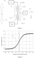
- Figure 2 shows the linear response of a GMR or MTJ magnetoresistive element.
- the output curve 13 When saturated, the output curve 13 will be in either the low resistance 14 R L or the high resistance 15 R H state.
- Response curve 13 in the area between the saturation fields varies linearly with the external magnetic field 19 (H).
- the external magnetic field 19 is applied parallel to the sensing axis 23.
- the magnetic field is negative (-H).
- the offset value is often referred to as "orange peel coupling" or “Neel coupling,” the typical value of this offset is usually between 1 and 40 Oe. It depends on the roughness of the MTJ element, making it dependent on materials and manufacturing processes.
- H S is the saturation field.
- H S is defined as the intersection between the linear region and the positive and negative saturation values, where the position is asymmetric due to H o .
- Figure 2 shows the ideal magnetoresistive response curve.
- the magnetoresistance R changes perfectly linearly with respect to applied field H, and there is no hysteresis (in actuality, the magnetoresistance shows a lag phenomenon, which is referred to as hysteresis; the magnetoresistive response curve for a full loop, often the hysteresis of common magnetoresistive materials is small, such that the response curve can be practically regarded as a straight line).
- the transfer curve 13 will not be truly linear.
- MTJ elements 1 can be connected in series to form an equivalent MTJ magnetoresistor with increased sensitivity, with a reduction of 1/F noise (which decreases as the number of MTJ elements 1 in series increases), while improving the ESD performance.
- the more complicated MTJ element array 20 is used as a magnetoresistive arm.
- the MTJ element 1 sits between the bottom electrode 9 and the top electrode 6 in a sandwich structure, wherein the current flows perpendicularly through the MTJ element 21 and flows horizontally in the top electrode layer 6 and the bottom electrode layer 9.
- Bottom electrode 9 is on the top of insulating layer 10, and insulating layer 10 is on the top of the substrate 11.
- a wire bond pad sits at the end of each string of MTJ elements making up a magnetoresistive arm. This is where other magnetoresistive arms or where the ohmmeter 34 or other electrical circuit components may be connected.
- the direction of current flow through the MTJ magnetoresistive arm 20 does not affect the value of the magnetoresistance or the resistance.
- the value of the resistance can be changed by changing the number of MTJ elements 1 in the magnetoresistive arm 20.
- Abridge circuit is often used to change the output resistance to a voltage than can be easily amplified. It can reduce the sensor noise, improve common mode rejection, reduce temperature drift and improve other deficiencies.
- the above mentioned MTJ arm 20 can be made into a bridge circuit.
- an MTJ element 1 is placed between two permanent magnets 22.
- Permanent magnets 22 have a gap 38 (Gap) between them, a width (W) 39, a thickness (1) 40 and length (L y ) 41.
- Permanent magnet 22 is designed to provide a cross-bias field (H cross ) 27 perpendicular to the sensitive axis 23 of the gradiometer.
- the magnetization of the permanent magnets 22 can be set by applying a large magnetic field, and the resulting field distribution 43 of the permanent magnets 22 is shown in Figure 5 .
- the magnetic field emanating from the edge 35 of the permanent magnets 22 is considered to arise from magnetic charges that form as a result of boundary conditions as shown schematically in Figure 6 .
- Equation 4 is a function of the width W 39 and gap G 38 shown in Figure 4 , so the saturation field of the MTJ element 1 can be changed by changing the dimensions of permanent magnets 22.
- H cross H mag sin ⁇ sns
- MTJ element 1 is generally patterned into a shape in order to provide shape anisotropy H k .
- the common shapes are long ellipse, long rectangle, rhomboid, etc.
- the response curve of the MTJ element can be modified.
- FIG. 7 schematically shows a half-bridge gradiometer configuration.
- the two MTJ elements R1 and R2 have the same sensing direction, configured as a half-bridge, the magnetoresistors are deposited on substrate 11 and insulating layer 10 which has electrical contacts, allowing for the formation of the gradiometer.
- the bridge electrical contacts There are many ways to connect to the bridge electrical contacts. These include the typical structure: integrated in-chip connections, wire-bonding, and solder-bumping.
- the permanent magnets 22 are tilted with respect to the MTJ elements 20. Between the two wire bond pads 28 and 29 a constant bias voltage V bias is applied.
- Arrow 8 represents the magnetization direction of the pinning layers 3 of the MTJ elements 20, wire-bond pad 30 provides the gradiometer output V OUT .
- the fields H CM and H dM are the common mode and differential mode output field values.
- the output does not change with H CM , it is only sensitive to the external magnetic field gradient, and this makes it insensitive to external magnetic field interference.
- V OUT R 2 ⁇ S R 2 H dM R 1 + S R 1 H dM + R 2 ⁇ S R 2 H dM ⁇ R 2 R 1 + R 2 V bias ,
- the half-bridge gradiometer in differential mode only responds to a gradient magnetic field, and outputs a signal proportional to it, but also has good magnetic field anti-interference capability.
- the measurement results of the described half-bridge gradiometer are shown in Figure 8 .
- the horizontal axis represents the gradient magnetic field. Because they are located at different locations, and the applied magnetic field has a gradient, the strength of the magnetic fields H1 and H2 at resistors R1 and R2 is different.
- CMRR 20 log S CM S dM
- CMRR is better than 40dB.
- FIG 9 shows the circuit diagram of a full-bridge magnetic field gradiometer
- Figure 10 shows the physical layout of the full bridge MTJ magnetic field gradiometer.
- each of the four magnetoresistive arms R1, R2, R3, R4 in the full bridge has the same sensitive direction.
- the magnetoresistors are deposited on the insulated substrate 10, 11 which is prepared with electrical contacts that can be used to electrically connect them.
- R1 and R4 are in same physical location on the chip, R2 and R3 are in the same physical location on the chip, all magnetoresistive arms in the bridge have the same sensitive direction, permanent magnets 22 are tilted and set around the MTJ elements 20, a bias voltage V bias is applied between bond-pads 28 and 29, the gradient of the external magnetic field H is measured along the sensitive direction 23, along the field direction the different pairs of MTJ magnetoresistive elements R1 and R2 (R3 and R4) show a different resistance change, arrow 8 shows the pinned layer magnetization direction for all four MTJ elements 20,
- the output terminals of the device 32 and 33 are representative of the voltage difference (V2-V1) and are the V OUT .
- V OUT only responds to the differential mode magnetic field H dM .
- V 1 ⁇ S R 2 ⁇ H dM 2 R 2
- V bias ⁇ S R H dM 2 R V bias
- V 2 R 4 + S R 4 H dM R 4 + S R 4 H dM + R 3 ⁇ S R 3 H dM ⁇ R 4 R 3 + R 4 V bias ⁇
- R is the resistance value of the MTJ elements 20
- S R is the sensitivity of the magnetoresistive elements. It can be shown that the full- and half-bridge magnetic field gradiometers have the same insensitivity to common mode magnetic fields, but the full-bridge has twice the sensitivity of the half-bridge magnetic field gradiometer. The typical output response of a full-bridge magnetic field gradiometer is shown in Figure 11 .
- the above mentioned half and full-bridge gradiometers can be prepared on single substrate using the same process steps. For this reason they can be called single-chip magnetoresistive magnetic field gradiometers. They are compatible with various different packaging techniques and can also be made multi-chip. For example, the magnetoresistive elements can be prepared on the same substrate using the same process steps, but then diced into separate chips that are electrically connected, resulting in full or half-bridge gradiometer devices. Whether single or multi-chip packaging is used, the external bond pads of the bridges may or may not be connected to an ASIC both of which would be placed on a lead frame, electrically connected to the output pins of the lead frame, and then encapsulated to form the packaged device.
Landscapes
- Physics & Mathematics (AREA)
- General Physics & Mathematics (AREA)
- Condensed Matter Physics & Semiconductors (AREA)
- Measuring Magnetic Variables (AREA)
- Hall/Mr Elements (AREA)
Claims (4)
- Capteur magnétorésistif à gradiomètre de champ magnétique, comprenant un pont magnétorésistif, dans lequel le pont magnétorésistif est un demi-pont,
dans lequel le pont magnétorésistif comprend :une multiplicité de bras magnétorésistifs (20) qui comprennent chacun un ou plusieurs éléments magnétorésistifs (1),les éléments capteurs magnétorésistifs (1) étant des éléments MTJ,les éléments magnétorésistifs (1) ayant une anisotropie de forme, etles éléments magnétorésistifs (1) étant formés sur le même substrat et ayant la même anisotropie de forme, la même valeur de résistance et la même sensibilité au champ magnétique,dans lequel chaque élément magnétorésistif (1) à l'intérieur du pont magnétorésistif possède une couche de fixation magnétique (3) avec un moment magnétique (8) aligné dans la même direction,des aimants permanents (22), dans lequel les éléments magnétorésistifs (1) sont chacun positionnés entre deux aimants permanents (22), dans lequel les aimants permanents sont réglés selon un angle d'orientation (44) par rapport à l'axe de sensibilité (23) du gradiomètre, dans lequel les aimants permanents sont configurés pour fournir un champ de polarisation croisée (Hcross 27) perpendiculaire à l'axe de sensibilité (23) du gradiomètre, et dans lequell'épaisseur (t) des aimants permanents, la direction (θmag 37) du moment magnétique des aimants permanents et l'angle d'orientation (θsns 44) des aimants permanents sont configurés pour générer un champ magnétique de polarisation (Hoff) qui définit à zéro le décalage (Ho) de la courbe de transfert (13) de chaque élément magnétorésistif (1),un substrat (11) sur lequel sont déposés le pont magnétorésistif et les aimants permanents (22), etdes plots de liaison filaires (28, 29, 30) utilisés pour interconnecter électriquement le capteur magnétorésistif à gradiomètre de champ magnétique à une puce ASIC ou à une borne d'une grille de connexion de boîtier par des fils de liaison. - Capteur magnétorésistif à gradiomètre de champ magnétique selon la revendication 1, dans lequel le pont magnétorésistif est un pont complet, comprenant une paire de demi-ponts connectés en parallèle, les bras magnétorésistifs ont la même direction de détection, et les bras magnétorésistifs sont répartis entre deux emplacements spatiaux séparés sur le substrat semi-conducteur, de telle sorte que les bras connectés en série ne se trouvent pas au même emplacement spatial sur le substrat semi-conducteur que les bras magnétorésistifs auxquels ils sont électriquement connectés, de sorte que le pont magnétorésistif soit configuré pour détecter un gradient de champ magnétique.
- Capteur magnétorésistif à gradiomètre de champ magnétique selon la revendication 1, dans lequel l'amplitude de la magnétisation est ajustée afin de commander les performances de sortie du gradiomètre magnétorésistif de champ magnétique.
- Capteur magnétorésistif à gradiomètre de champ magnétique selon la revendication 1, dans lequel le gradiomètre magnétorésistif de champ magnétique est un gradiomètre magnétorésistif de champ magnétique à puce unique.
Applications Claiming Priority (2)
| Application Number | Priority Date | Filing Date | Title |
|---|---|---|---|
| CN201210065925.5A CN102590768B (zh) | 2012-03-14 | 2012-03-14 | 一种磁电阻磁场梯度传感器 |
| PCT/CN2013/071090 WO2013135117A1 (fr) | 2012-03-14 | 2013-01-29 | Capteur magnétorésistif à gradient de champ magnétique |
Publications (3)
| Publication Number | Publication Date |
|---|---|
| EP2827165A1 EP2827165A1 (fr) | 2015-01-21 |
| EP2827165A4 EP2827165A4 (fr) | 2016-01-20 |
| EP2827165B1 true EP2827165B1 (fr) | 2024-07-17 |
Family
ID=46479687
Family Applications (1)
| Application Number | Title | Priority Date | Filing Date |
|---|---|---|---|
| EP13761465.7A Active EP2827165B1 (fr) | 2012-03-14 | 2013-01-29 | Capteur magnétorésistif à gradient de champ magnétique |
Country Status (5)
| Country | Link |
|---|---|
| US (1) | US9678178B2 (fr) |
| EP (1) | EP2827165B1 (fr) |
| JP (1) | JP2015511705A (fr) |
| CN (1) | CN102590768B (fr) |
| WO (1) | WO2013135117A1 (fr) |
Families Citing this family (43)
| Publication number | Priority date | Publication date | Assignee | Title |
|---|---|---|---|---|
| CN102565727B (zh) * | 2012-02-20 | 2016-01-20 | 江苏多维科技有限公司 | 用于测量磁场的磁电阻传感器 |
| CN102590768B (zh) | 2012-03-14 | 2014-04-16 | 江苏多维科技有限公司 | 一种磁电阻磁场梯度传感器 |
| CN102890175B (zh) * | 2012-10-24 | 2015-07-01 | 无锡乐尔科技有限公司 | 用于电流传感器的磁电阻集成芯片 |
| CN102901858B (zh) * | 2012-10-24 | 2015-08-19 | 无锡乐尔科技有限公司 | 一种电流传感器 |
| CN203133257U (zh) * | 2013-03-18 | 2013-08-14 | 江苏多维科技有限公司 | 用于验钞机磁头的tmr半桥磁场梯度传感器芯片 |
| CN103499271A (zh) * | 2013-09-29 | 2014-01-08 | 无锡乐尔科技有限公司 | 一种厚度测量装置 |
| CN103792501B (zh) * | 2014-01-22 | 2016-03-30 | 中国人民解放军国防科学技术大学 | 一种桥接式石墨烯基磁传感器 |
| JP2017096627A (ja) * | 2014-03-28 | 2017-06-01 | コニカミノルタ株式会社 | 磁気センサー |
| CN103995240B (zh) * | 2014-05-30 | 2017-11-10 | 江苏多维科技有限公司 | 一种磁电阻z轴梯度传感器芯片 |
| JP6352195B2 (ja) * | 2015-01-14 | 2018-07-04 | Tdk株式会社 | 磁気センサ |
| CN104614689A (zh) * | 2015-01-22 | 2015-05-13 | 北京航空航天大学 | 一种基于巨磁阻抗效应的磁场梯度传感器 |
| CN110045303B (zh) * | 2015-05-08 | 2021-12-14 | 爱盛科技股份有限公司 | 磁场感测模块 |
| CN105044631B (zh) * | 2015-08-28 | 2018-08-07 | 江苏多维科技有限公司 | 一种半翻转两轴线性磁电阻传感器 |
| RU2642887C1 (ru) * | 2017-04-11 | 2018-01-29 | Федеральное государственное бюджетное образовательное учреждение высшего образования "Омский государственный технический университет" | Градиентометр напряженности магнитного поля |
| JP6485491B2 (ja) * | 2017-06-08 | 2019-03-20 | Tdk株式会社 | 磁気センサ及びカメラモジュール |
| CN107290694B (zh) * | 2017-07-18 | 2020-12-18 | 上海交通大学 | 抑制方向串扰的电感型磁传感器及其制备方法 |
| CN208143202U (zh) * | 2017-12-15 | 2018-11-23 | 江苏多维科技有限公司 | 一种基于磁电阻的双稳态磁开关及系统 |
| US10693056B2 (en) | 2017-12-28 | 2020-06-23 | Spin Memory, Inc. | Three-dimensional (3D) magnetic memory device comprising a magnetic tunnel junction (MTJ) having a metallic buffer layer |
| US10403343B2 (en) * | 2017-12-29 | 2019-09-03 | Spin Memory, Inc. | Systems and methods utilizing serial configurations of magnetic memory devices |
| US10803916B2 (en) | 2017-12-29 | 2020-10-13 | Spin Memory, Inc. | Methods and systems for writing to magnetic memory devices utilizing alternating current |
| US10424357B2 (en) | 2017-12-29 | 2019-09-24 | Spin Memory, Inc. | Magnetic tunnel junction (MTJ) memory device having a composite free magnetic layer |
| US10347308B1 (en) | 2017-12-29 | 2019-07-09 | Spin Memory, Inc. | Systems and methods utilizing parallel configurations of magnetic memory devices |
| US10192789B1 (en) | 2018-01-08 | 2019-01-29 | Spin Transfer Technologies | Methods of fabricating dual threshold voltage devices |
| US10319424B1 (en) | 2018-01-08 | 2019-06-11 | Spin Memory, Inc. | Adjustable current selectors |
| CN112769498B (zh) * | 2018-09-26 | 2022-04-26 | 武汉信跃致科技有限公司 | 一种无线通信分析仪器及使用方法 |
| US10692556B2 (en) | 2018-09-28 | 2020-06-23 | Spin Memory, Inc. | Defect injection structure and mechanism for magnetic memory |
| US10878870B2 (en) | 2018-09-28 | 2020-12-29 | Spin Memory, Inc. | Defect propagation structure and mechanism for magnetic memory |
| DE102019112190A1 (de) * | 2019-05-09 | 2020-11-12 | Mack Rides Gmbh & Co. Kg | Sperrvorrichtung eines Sicherheitsbügels, Fahrgastaufnahme sowie Vergnügungsfahrgeschäft mit einer solchen Sperrvorrichtung |
| JP2021043003A (ja) * | 2019-09-09 | 2021-03-18 | パナソニックIpマネジメント株式会社 | 磁気式位置検出装置 |
| TWI705262B (zh) * | 2019-09-27 | 2020-09-21 | 愛盛科技股份有限公司 | 磁場感測裝置 |
| RU2725651C1 (ru) * | 2019-11-05 | 2020-07-03 | ООО "Энергосервис" | Градиент напряженности магнитного поля |
| CN111060862B (zh) * | 2019-12-09 | 2022-04-05 | 中国船舶重工集团有限公司第七一0研究所 | 一种磁场方向和梯度方向夹角可调的二维梯度磁场系统 |
| CN112363097B (zh) * | 2020-11-02 | 2021-09-21 | 珠海多创科技有限公司 | 磁电阻传感器芯片 |
| CN112577531B (zh) * | 2020-11-05 | 2022-01-21 | 北京麦格纳材科技有限公司 | 一种磁传感器芯片抗电磁干扰结构及其制备方法 |
| CN113063344B (zh) * | 2021-03-19 | 2022-10-11 | 江苏多维科技有限公司 | 一种低磁场磁电阻角度传感器 |
| CN114089234B (zh) * | 2021-11-08 | 2024-06-04 | 中国科学院电工研究所 | 一种超导磁悬浮场的磁力梯度测量方法及测量装置 |
| CN114509593B (zh) * | 2021-12-31 | 2024-11-26 | 歌尔微电子股份有限公司 | 电流传感器、电子设备和检测装置 |
| CN114839418A (zh) * | 2021-12-31 | 2022-08-02 | 歌尔微电子股份有限公司 | 传感器、电子设备和检测装置 |
| CN114895093B (zh) * | 2022-04-14 | 2025-07-11 | 珠海多创科技有限公司 | 一种拓扑识别接收模块 |
| CN114706025B (zh) * | 2022-04-15 | 2024-03-22 | 深圳技术大学 | 一种基于磁电效应的谐振式dc磁传感器 |
| CN117110956B (zh) * | 2023-08-17 | 2025-10-10 | 美新半导体(无锡)有限公司 | Tmr磁传感器 |
| CN117177654B (zh) * | 2023-08-28 | 2024-03-29 | 珠海多创科技有限公司 | 一种磁阻元件及其制备方法、电子设备 |
| CN117054936B (zh) * | 2023-10-12 | 2024-01-12 | 江苏多维科技有限公司 | 一种梯度传感器 |
Citations (8)
| Publication number | Priority date | Publication date | Assignee | Title |
|---|---|---|---|---|
| US20040046624A1 (en) * | 2001-06-09 | 2004-03-11 | Peter Schmollngruber | Magneto-resistive layer arrangement and gradiometer with said layer arrangement |
| US20050073301A1 (en) * | 2002-03-28 | 2005-04-07 | Ingo Herrmann | Sensor element and gradiometer assemblage, use thereof for measuring magnetic field gradients, and method therefor |
| US6956366B2 (en) * | 2002-03-07 | 2005-10-18 | Koninklijke Philips Electronics N.V. | Arrangement for determining the position of a motion sensor element influencing the formation of a magnetic field of a working magnet along its motion coordinate |
| CN202013413U (zh) * | 2011-04-06 | 2011-10-19 | 江苏多维科技有限公司 | 单一芯片桥式磁场传感器 |
| CN102226836A (zh) * | 2011-04-06 | 2011-10-26 | 江苏多维科技有限公司 | 单一芯片桥式磁场传感器及其制备方法 |
| CN102298124A (zh) * | 2011-03-03 | 2011-12-28 | 江苏多维科技有限公司 | 一种独立封装的桥式磁场角度传感器 |
| EP2700968A1 (fr) * | 2011-04-21 | 2014-02-26 | Jiangsu MultiDimension Technology Co. Ltd | Capteur de champ magnétique en pont complet à référence monopuce |
| EP2818884A1 (fr) * | 2012-02-20 | 2014-12-31 | Jiangsu Multidimensional Technology Co., Ltd | Capteur magnéto-résistif pour mesurer un champ magnétique |
Family Cites Families (20)
| Publication number | Priority date | Publication date | Assignee | Title |
|---|---|---|---|---|
| JPH06148301A (ja) * | 1992-05-15 | 1994-05-27 | Fujitsu Ltd | 磁気センサ |
| JP3089828B2 (ja) * | 1992-05-27 | 2000-09-18 | 株式会社村田製作所 | 強磁性磁気抵抗素子 |
| US5561368A (en) * | 1994-11-04 | 1996-10-01 | International Business Machines Corporation | Bridge circuit magnetic field sensor having spin valve magnetoresistive elements formed on common substrate |
| JP3498737B2 (ja) * | 2001-01-24 | 2004-02-16 | ヤマハ株式会社 | 磁気センサの製造方法 |
| US7390584B2 (en) * | 2002-03-27 | 2008-06-24 | Nve Corporation | Spin dependent tunneling devices having reduced topological coupling |
| JP2003318463A (ja) * | 2002-04-23 | 2003-11-07 | Alps Electric Co Ltd | 交換結合膜及びこの交換結合膜の製造方法並びに前記交換結合膜を用いた磁気検出素子 |
| US6833697B2 (en) * | 2002-09-11 | 2004-12-21 | Honeywell International Inc. | Saturated magnetoresistive approach for linear position sensing |
| KR100698413B1 (ko) * | 2004-09-28 | 2007-03-23 | 야마하 가부시키가이샤 | 거대 자기저항 소자를 이용한 자기 센서 및 그 제조 방법 |
| JP4466487B2 (ja) * | 2005-06-27 | 2010-05-26 | Tdk株式会社 | 磁気センサおよび電流センサ |
| EP1989564B1 (fr) | 2006-02-23 | 2010-09-29 | Nxp B.V. | Dispositif de capteur magnétorésistif et procédé de fabrication d'un tel dispositif de capteur magnétorésistif |
| DE102006032277B4 (de) * | 2006-07-12 | 2017-06-01 | Infineon Technologies Ag | Magnetfeldsensorbauelement |
| JP4798498B2 (ja) * | 2006-12-14 | 2011-10-19 | 日立金属株式会社 | 磁気センサーおよび磁気エンコーダー |
| JP4768066B2 (ja) * | 2007-03-20 | 2011-09-07 | アルプス電気株式会社 | 磁気抵抗効果素子を用いた位置検知装置 |
| US7635974B2 (en) | 2007-05-02 | 2009-12-22 | Magic Technologies, Inc. | Magnetic tunnel junction (MTJ) based magnetic field angle sensor |
| DE102007032867B4 (de) * | 2007-07-13 | 2009-12-24 | Infineon Technologies Ag | Magnetoresistive Magnetfeldsensorstrukturen und Herstellungsverfahren |
| JP5066579B2 (ja) * | 2007-12-28 | 2012-11-07 | アルプス電気株式会社 | 磁気センサ及び磁気センサモジュール |
| CN102297652B (zh) | 2011-03-03 | 2012-12-05 | 江苏多维科技有限公司 | 一种独立封装的磁电阻角度传感器 |
| CN102226835A (zh) | 2011-04-06 | 2011-10-26 | 江苏多维科技有限公司 | 单一芯片双轴磁场传感器及其制备方法 |
| CN202794487U (zh) * | 2012-03-14 | 2013-03-13 | 江苏多维科技有限公司 | 一种磁电阻磁场梯度传感器 |
| CN102590768B (zh) * | 2012-03-14 | 2014-04-16 | 江苏多维科技有限公司 | 一种磁电阻磁场梯度传感器 |
-
2012
- 2012-03-14 CN CN201210065925.5A patent/CN102590768B/zh active Active
-
2013
- 2013-01-29 US US14/384,666 patent/US9678178B2/en active Active
- 2013-01-29 EP EP13761465.7A patent/EP2827165B1/fr active Active
- 2013-01-29 JP JP2014561268A patent/JP2015511705A/ja active Pending
- 2013-01-29 WO PCT/CN2013/071090 patent/WO2013135117A1/fr not_active Ceased
Patent Citations (8)
| Publication number | Priority date | Publication date | Assignee | Title |
|---|---|---|---|---|
| US20040046624A1 (en) * | 2001-06-09 | 2004-03-11 | Peter Schmollngruber | Magneto-resistive layer arrangement and gradiometer with said layer arrangement |
| US6956366B2 (en) * | 2002-03-07 | 2005-10-18 | Koninklijke Philips Electronics N.V. | Arrangement for determining the position of a motion sensor element influencing the formation of a magnetic field of a working magnet along its motion coordinate |
| US20050073301A1 (en) * | 2002-03-28 | 2005-04-07 | Ingo Herrmann | Sensor element and gradiometer assemblage, use thereof for measuring magnetic field gradients, and method therefor |
| CN102298124A (zh) * | 2011-03-03 | 2011-12-28 | 江苏多维科技有限公司 | 一种独立封装的桥式磁场角度传感器 |
| CN202013413U (zh) * | 2011-04-06 | 2011-10-19 | 江苏多维科技有限公司 | 单一芯片桥式磁场传感器 |
| CN102226836A (zh) * | 2011-04-06 | 2011-10-26 | 江苏多维科技有限公司 | 单一芯片桥式磁场传感器及其制备方法 |
| EP2700968A1 (fr) * | 2011-04-21 | 2014-02-26 | Jiangsu MultiDimension Technology Co. Ltd | Capteur de champ magnétique en pont complet à référence monopuce |
| EP2818884A1 (fr) * | 2012-02-20 | 2014-12-31 | Jiangsu Multidimensional Technology Co., Ltd | Capteur magnéto-résistif pour mesurer un champ magnétique |
Also Published As
| Publication number | Publication date |
|---|---|
| US20150130455A1 (en) | 2015-05-14 |
| EP2827165A4 (fr) | 2016-01-20 |
| CN102590768A (zh) | 2012-07-18 |
| US9678178B2 (en) | 2017-06-13 |
| JP2015511705A (ja) | 2015-04-20 |
| CN102590768B (zh) | 2014-04-16 |
| WO2013135117A1 (fr) | 2013-09-19 |
| EP2827165A1 (fr) | 2015-01-21 |
Similar Documents
| Publication | Publication Date | Title |
|---|---|---|
| EP2827165B1 (fr) | Capteur magnétorésistif à gradient de champ magnétique | |
| JP6420665B2 (ja) | 磁場を測定する磁気抵抗センサ | |
| US9664754B2 (en) | Single chip push-pull bridge-type magnetic field sensor | |
| US9465056B2 (en) | Current sensor with temperature-compensated magnetic tunnel junction bridge | |
| US10060941B2 (en) | Magnetoresistive gear tooth sensor | |
| US9123877B2 (en) | Single-chip bridge-type magnetic field sensor and preparation method thereof | |
| US8373536B2 (en) | Integrated lateral short circuit for a beneficial modification of current distribution structure for xMR magnetoresistive sensors | |
| EP2752675B1 (fr) | Capteur de champ magnétique à axe triple mtj et son procédé d'encapsulation | |
| EP2682773B1 (fr) | Capteur d'angle de champ magnétique à pont enrobé séparément | |
| CN102298126B (zh) | 独立封装的桥式磁场传感器 | |
| JP6509231B2 (ja) | 強磁場用のシングルチップ基準ブリッジ磁気センサ | |
| CN102540112B (zh) | 单一芯片推挽桥式磁场传感器 | |
| CN102621504A (zh) | 单片参考全桥磁场传感器 | |
| CN103901363A (zh) | 一种单芯片z轴线性磁阻传感器 | |
| JP2017502298A5 (fr) | ||
| CN202794487U (zh) | 一种磁电阻磁场梯度传感器 | |
| CN202494772U (zh) | 用于测量磁场的磁电阻传感器 |
Legal Events
| Date | Code | Title | Description |
|---|---|---|---|
| PUAI | Public reference made under article 153(3) epc to a published international application that has entered the european phase |
Free format text: ORIGINAL CODE: 0009012 |
|
| 17P | Request for examination filed |
Effective date: 20141014 |
|
| AK | Designated contracting states |
Kind code of ref document: A1 Designated state(s): AL AT BE BG CH CY CZ DE DK EE ES FI FR GB GR HR HU IE IS IT LI LT LU LV MC MK MT NL NO PL PT RO RS SE SI SK SM TR |
|
| AX | Request for extension of the european patent |
Extension state: BA ME |
|
| DAX | Request for extension of the european patent (deleted) | ||
| RAP1 | Party data changed (applicant data changed or rights of an application transferred) |
Owner name: MULTIDIMENSION TECHNOLOGY CO., LTD. |
|
| RA4 | Supplementary search report drawn up and despatched (corrected) |
Effective date: 20151222 |
|
| RIC1 | Information provided on ipc code assigned before grant |
Ipc: G01R 33/09 20060101ALI20151216BHEP Ipc: G01R 33/02 20060101AFI20151216BHEP |
|
| STAA | Information on the status of an ep patent application or granted ep patent |
Free format text: STATUS: EXAMINATION IS IN PROGRESS |
|
| 17Q | First examination report despatched |
Effective date: 20190711 |
|
| RAP3 | Party data changed (applicant data changed or rights of an application transferred) |
Owner name: MULTIDIMENSION TECHNOLOGY CO., LTD. |
|
| RIN1 | Information on inventor provided before grant (corrected) |
Inventor name: SHEN, WEIFENG Inventor name: LIU, MINGFENG Inventor name: DEAK, JAMES GEZA Inventor name: BAI, JIANJUN |
|
| P01 | Opt-out of the competence of the unified patent court (upc) registered |
Effective date: 20230626 |
|
| GRAP | Despatch of communication of intention to grant a patent |
Free format text: ORIGINAL CODE: EPIDOSNIGR1 |
|
| STAA | Information on the status of an ep patent application or granted ep patent |
Free format text: STATUS: GRANT OF PATENT IS INTENDED |
|
| RIC1 | Information provided on ipc code assigned before grant |
Ipc: G01R 33/022 20060101ALI20240131BHEP Ipc: G01R 33/09 20060101ALI20240131BHEP Ipc: G01R 33/02 20060101AFI20240131BHEP |
|
| INTG | Intention to grant announced |
Effective date: 20240214 |
|
| GRAS | Grant fee paid |
Free format text: ORIGINAL CODE: EPIDOSNIGR3 |
|
| GRAA | (expected) grant |
Free format text: ORIGINAL CODE: 0009210 |
|
| STAA | Information on the status of an ep patent application or granted ep patent |
Free format text: STATUS: THE PATENT HAS BEEN GRANTED |
|
| RIN1 | Information on inventor provided before grant (corrected) |
Inventor name: SHEN, WEIFENG Inventor name: LIU, MINGFENG Inventor name: DEAK, JAMES GEZA Inventor name: BAI, JIANMIN |
|
| AK | Designated contracting states |
Kind code of ref document: B1 Designated state(s): AL AT BE BG CH CY CZ DE DK EE ES FI FR GB GR HR HU IE IS IT LI LT LU LV MC MK MT NL NO PL PT RO RS SE SI SK SM TR |
|
| REG | Reference to a national code |
Ref country code: GB Ref legal event code: FG4D |
|
| REG | Reference to a national code |
Ref country code: CH Ref legal event code: EP |
|
| REG | Reference to a national code |
Ref country code: DE Ref legal event code: R096 Ref document number: 602013085911 Country of ref document: DE |
|
| REG | Reference to a national code |
Ref country code: IE Ref legal event code: FG4D |
|
| REG | Reference to a national code |
Ref country code: LT Ref legal event code: MG9D |
|
| REG | Reference to a national code |
Ref country code: NL Ref legal event code: MP Effective date: 20240717 |
|
| PG25 | Lapsed in a contracting state [announced via postgrant information from national office to epo] |
Ref country code: PT Free format text: LAPSE BECAUSE OF FAILURE TO SUBMIT A TRANSLATION OF THE DESCRIPTION OR TO PAY THE FEE WITHIN THE PRESCRIBED TIME-LIMIT Effective date: 20241118 |
|
| REG | Reference to a national code |
Ref country code: AT Ref legal event code: MK05 Ref document number: 1704631 Country of ref document: AT Kind code of ref document: T Effective date: 20240717 |
|
| PG25 | Lapsed in a contracting state [announced via postgrant information from national office to epo] |
Ref country code: NL Free format text: LAPSE BECAUSE OF FAILURE TO SUBMIT A TRANSLATION OF THE DESCRIPTION OR TO PAY THE FEE WITHIN THE PRESCRIBED TIME-LIMIT Effective date: 20240717 |
|
| PG25 | Lapsed in a contracting state [announced via postgrant information from national office to epo] |
Ref country code: PT Free format text: LAPSE BECAUSE OF FAILURE TO SUBMIT A TRANSLATION OF THE DESCRIPTION OR TO PAY THE FEE WITHIN THE PRESCRIBED TIME-LIMIT Effective date: 20241118 Ref country code: NL Free format text: LAPSE BECAUSE OF FAILURE TO SUBMIT A TRANSLATION OF THE DESCRIPTION OR TO PAY THE FEE WITHIN THE PRESCRIBED TIME-LIMIT Effective date: 20240717 |
|
| PG25 | Lapsed in a contracting state [announced via postgrant information from national office to epo] |
Ref country code: NO Free format text: LAPSE BECAUSE OF FAILURE TO SUBMIT A TRANSLATION OF THE DESCRIPTION OR TO PAY THE FEE WITHIN THE PRESCRIBED TIME-LIMIT Effective date: 20241017 |
|
| PG25 | Lapsed in a contracting state [announced via postgrant information from national office to epo] |
Ref country code: PL Free format text: LAPSE BECAUSE OF FAILURE TO SUBMIT A TRANSLATION OF THE DESCRIPTION OR TO PAY THE FEE WITHIN THE PRESCRIBED TIME-LIMIT Effective date: 20240717 Ref country code: FI Free format text: LAPSE BECAUSE OF FAILURE TO SUBMIT A TRANSLATION OF THE DESCRIPTION OR TO PAY THE FEE WITHIN THE PRESCRIBED TIME-LIMIT Effective date: 20240717 Ref country code: GR Free format text: LAPSE BECAUSE OF FAILURE TO SUBMIT A TRANSLATION OF THE DESCRIPTION OR TO PAY THE FEE WITHIN THE PRESCRIBED TIME-LIMIT Effective date: 20241018 |
|
| PG25 | Lapsed in a contracting state [announced via postgrant information from national office to epo] |
Ref country code: BG Free format text: LAPSE BECAUSE OF FAILURE TO SUBMIT A TRANSLATION OF THE DESCRIPTION OR TO PAY THE FEE WITHIN THE PRESCRIBED TIME-LIMIT Effective date: 20240717 |
|
| PG25 | Lapsed in a contracting state [announced via postgrant information from national office to epo] |
Ref country code: LV Free format text: LAPSE BECAUSE OF FAILURE TO SUBMIT A TRANSLATION OF THE DESCRIPTION OR TO PAY THE FEE WITHIN THE PRESCRIBED TIME-LIMIT Effective date: 20240717 |
|
| PG25 | Lapsed in a contracting state [announced via postgrant information from national office to epo] |
Ref country code: AT Free format text: LAPSE BECAUSE OF FAILURE TO SUBMIT A TRANSLATION OF THE DESCRIPTION OR TO PAY THE FEE WITHIN THE PRESCRIBED TIME-LIMIT Effective date: 20240717 Ref country code: IS Free format text: LAPSE BECAUSE OF FAILURE TO SUBMIT A TRANSLATION OF THE DESCRIPTION OR TO PAY THE FEE WITHIN THE PRESCRIBED TIME-LIMIT Effective date: 20241117 |
|
| PG25 | Lapsed in a contracting state [announced via postgrant information from national office to epo] |
Ref country code: HR Free format text: LAPSE BECAUSE OF FAILURE TO SUBMIT A TRANSLATION OF THE DESCRIPTION OR TO PAY THE FEE WITHIN THE PRESCRIBED TIME-LIMIT Effective date: 20240717 |
|
| PG25 | Lapsed in a contracting state [announced via postgrant information from national office to epo] |
Ref country code: ES Free format text: LAPSE BECAUSE OF FAILURE TO SUBMIT A TRANSLATION OF THE DESCRIPTION OR TO PAY THE FEE WITHIN THE PRESCRIBED TIME-LIMIT Effective date: 20240717 Ref country code: RS Free format text: LAPSE BECAUSE OF FAILURE TO SUBMIT A TRANSLATION OF THE DESCRIPTION OR TO PAY THE FEE WITHIN THE PRESCRIBED TIME-LIMIT Effective date: 20241017 |
|
| PG25 | Lapsed in a contracting state [announced via postgrant information from national office to epo] |
Ref country code: RS Free format text: LAPSE BECAUSE OF FAILURE TO SUBMIT A TRANSLATION OF THE DESCRIPTION OR TO PAY THE FEE WITHIN THE PRESCRIBED TIME-LIMIT Effective date: 20241017 Ref country code: PL Free format text: LAPSE BECAUSE OF FAILURE TO SUBMIT A TRANSLATION OF THE DESCRIPTION OR TO PAY THE FEE WITHIN THE PRESCRIBED TIME-LIMIT Effective date: 20240717 Ref country code: NO Free format text: LAPSE BECAUSE OF FAILURE TO SUBMIT A TRANSLATION OF THE DESCRIPTION OR TO PAY THE FEE WITHIN THE PRESCRIBED TIME-LIMIT Effective date: 20241017 Ref country code: LV Free format text: LAPSE BECAUSE OF FAILURE TO SUBMIT A TRANSLATION OF THE DESCRIPTION OR TO PAY THE FEE WITHIN THE PRESCRIBED TIME-LIMIT Effective date: 20240717 Ref country code: IS Free format text: LAPSE BECAUSE OF FAILURE TO SUBMIT A TRANSLATION OF THE DESCRIPTION OR TO PAY THE FEE WITHIN THE PRESCRIBED TIME-LIMIT Effective date: 20241117 Ref country code: HR Free format text: LAPSE BECAUSE OF FAILURE TO SUBMIT A TRANSLATION OF THE DESCRIPTION OR TO PAY THE FEE WITHIN THE PRESCRIBED TIME-LIMIT Effective date: 20240717 Ref country code: GR Free format text: LAPSE BECAUSE OF FAILURE TO SUBMIT A TRANSLATION OF THE DESCRIPTION OR TO PAY THE FEE WITHIN THE PRESCRIBED TIME-LIMIT Effective date: 20241018 Ref country code: FI Free format text: LAPSE BECAUSE OF FAILURE TO SUBMIT A TRANSLATION OF THE DESCRIPTION OR TO PAY THE FEE WITHIN THE PRESCRIBED TIME-LIMIT Effective date: 20240717 Ref country code: ES Free format text: LAPSE BECAUSE OF FAILURE TO SUBMIT A TRANSLATION OF THE DESCRIPTION OR TO PAY THE FEE WITHIN THE PRESCRIBED TIME-LIMIT Effective date: 20240717 Ref country code: BG Free format text: LAPSE BECAUSE OF FAILURE TO SUBMIT A TRANSLATION OF THE DESCRIPTION OR TO PAY THE FEE WITHIN THE PRESCRIBED TIME-LIMIT Effective date: 20240717 Ref country code: AT Free format text: LAPSE BECAUSE OF FAILURE TO SUBMIT A TRANSLATION OF THE DESCRIPTION OR TO PAY THE FEE WITHIN THE PRESCRIBED TIME-LIMIT Effective date: 20240717 |
|
| PG25 | Lapsed in a contracting state [announced via postgrant information from national office to epo] |
Ref country code: RO Free format text: LAPSE BECAUSE OF FAILURE TO SUBMIT A TRANSLATION OF THE DESCRIPTION OR TO PAY THE FEE WITHIN THE PRESCRIBED TIME-LIMIT Effective date: 20240717 Ref country code: DK Free format text: LAPSE BECAUSE OF FAILURE TO SUBMIT A TRANSLATION OF THE DESCRIPTION OR TO PAY THE FEE WITHIN THE PRESCRIBED TIME-LIMIT Effective date: 20240717 Ref country code: SM Free format text: LAPSE BECAUSE OF FAILURE TO SUBMIT A TRANSLATION OF THE DESCRIPTION OR TO PAY THE FEE WITHIN THE PRESCRIBED TIME-LIMIT Effective date: 20240717 |
|
| REG | Reference to a national code |
Ref country code: DE Ref legal event code: R097 Ref document number: 602013085911 Country of ref document: DE |
|
| PG25 | Lapsed in a contracting state [announced via postgrant information from national office to epo] |
Ref country code: EE Free format text: LAPSE BECAUSE OF FAILURE TO SUBMIT A TRANSLATION OF THE DESCRIPTION OR TO PAY THE FEE WITHIN THE PRESCRIBED TIME-LIMIT Effective date: 20240717 |
|
| PG25 | Lapsed in a contracting state [announced via postgrant information from national office to epo] |
Ref country code: CZ Free format text: LAPSE BECAUSE OF FAILURE TO SUBMIT A TRANSLATION OF THE DESCRIPTION OR TO PAY THE FEE WITHIN THE PRESCRIBED TIME-LIMIT Effective date: 20240717 |
|
| PG25 | Lapsed in a contracting state [announced via postgrant information from national office to epo] |
Ref country code: SK Free format text: LAPSE BECAUSE OF FAILURE TO SUBMIT A TRANSLATION OF THE DESCRIPTION OR TO PAY THE FEE WITHIN THE PRESCRIBED TIME-LIMIT Effective date: 20240717 |
|
| PLBE | No opposition filed within time limit |
Free format text: ORIGINAL CODE: 0009261 |
|
| STAA | Information on the status of an ep patent application or granted ep patent |
Free format text: STATUS: NO OPPOSITION FILED WITHIN TIME LIMIT |
|
| 26N | No opposition filed |
Effective date: 20250422 |
|
| REG | Reference to a national code |
Ref country code: CH Ref legal event code: PL |
|
| PG25 | Lapsed in a contracting state [announced via postgrant information from national office to epo] |
Ref country code: SE Free format text: LAPSE BECAUSE OF FAILURE TO SUBMIT A TRANSLATION OF THE DESCRIPTION OR TO PAY THE FEE WITHIN THE PRESCRIBED TIME-LIMIT Effective date: 20240717 |
|
| PG25 | Lapsed in a contracting state [announced via postgrant information from national office to epo] |
Ref country code: MC Free format text: LAPSE BECAUSE OF FAILURE TO SUBMIT A TRANSLATION OF THE DESCRIPTION OR TO PAY THE FEE WITHIN THE PRESCRIBED TIME-LIMIT Effective date: 20240717 Ref country code: LU Free format text: LAPSE BECAUSE OF NON-PAYMENT OF DUE FEES Effective date: 20250129 |
|
| PG25 | Lapsed in a contracting state [announced via postgrant information from national office to epo] |
Ref country code: BE Free format text: LAPSE BECAUSE OF NON-PAYMENT OF DUE FEES Effective date: 20250131 |
|
| PG25 | Lapsed in a contracting state [announced via postgrant information from national office to epo] |
Ref country code: CH Free format text: LAPSE BECAUSE OF NON-PAYMENT OF DUE FEES Effective date: 20250131 |
|
| REG | Reference to a national code |
Ref country code: BE Ref legal event code: MM Effective date: 20250131 |
|
| PG25 | Lapsed in a contracting state [announced via postgrant information from national office to epo] |
Ref country code: IE Free format text: LAPSE BECAUSE OF NON-PAYMENT OF DUE FEES Effective date: 20250129 |
|
| PG25 | Lapsed in a contracting state [announced via postgrant information from national office to epo] |
Ref country code: IT Free format text: LAPSE BECAUSE OF FAILURE TO SUBMIT A TRANSLATION OF THE DESCRIPTION OR TO PAY THE FEE WITHIN THE PRESCRIBED TIME-LIMIT Effective date: 20240717 |
|
| PGFP | Annual fee paid to national office [announced via postgrant information from national office to epo] |
Ref country code: GB Payment date: 20260127 Year of fee payment: 14 |
|
| PGFP | Annual fee paid to national office [announced via postgrant information from national office to epo] |
Ref country code: DE Payment date: 20260128 Year of fee payment: 14 |
|
| PGFP | Annual fee paid to national office [announced via postgrant information from national office to epo] |
Ref country code: FR Payment date: 20260126 Year of fee payment: 14 |