EP2827177B1 - Antireflexionsfolie - Google Patents
Antireflexionsfolie Download PDFInfo
- Publication number
- EP2827177B1 EP2827177B1 EP13760782.6A EP13760782A EP2827177B1 EP 2827177 B1 EP2827177 B1 EP 2827177B1 EP 13760782 A EP13760782 A EP 13760782A EP 2827177 B1 EP2827177 B1 EP 2827177B1
- Authority
- EP
- European Patent Office
- Prior art keywords
- antireflection film
- protective
- protrusions
- protrusion
- pillars
- Prior art date
- Legal status (The legal status is an assumption and is not a legal conclusion. Google has not performed a legal analysis and makes no representation as to the accuracy of the status listed.)
- Not-in-force
Links
- 230000003287 optical effect Effects 0.000 claims description 38
- 239000000463 material Substances 0.000 claims description 37
- 239000004973 liquid crystal related substance Substances 0.000 claims description 18
- 230000007423 decrease Effects 0.000 claims description 5
- 230000001681 protective effect Effects 0.000 description 153
- 239000011295 pitch Substances 0.000 description 14
- 238000010586 diagram Methods 0.000 description 8
- 230000001373 regressive effect Effects 0.000 description 8
- 238000001000 micrograph Methods 0.000 description 6
- 238000007796 conventional method Methods 0.000 description 5
- 230000000694 effects Effects 0.000 description 5
- 239000011347 resin Substances 0.000 description 5
- 229920005989 resin Polymers 0.000 description 5
- 230000000994 depressogenic effect Effects 0.000 description 4
- 230000002093 peripheral effect Effects 0.000 description 4
- 229920000535 Tan II Polymers 0.000 description 3
- 210000002374 sebum Anatomy 0.000 description 3
- 239000004925 Acrylic resin Substances 0.000 description 2
- 230000001174 ascending effect Effects 0.000 description 2
- 239000000470 constituent Substances 0.000 description 2
- 238000013461 design Methods 0.000 description 2
- 230000003760 hair shine Effects 0.000 description 2
- 239000002105 nanoparticle Substances 0.000 description 2
- 229920005668 polycarbonate resin Polymers 0.000 description 2
- 239000004431 polycarbonate resin Substances 0.000 description 2
- 230000000007 visual effect Effects 0.000 description 2
- 206010000496 acne Diseases 0.000 description 1
- 239000003086 colorant Substances 0.000 description 1
- 230000001419 dependent effect Effects 0.000 description 1
- 230000002542 deteriorative effect Effects 0.000 description 1
- 238000002474 experimental method Methods 0.000 description 1
- 239000004744 fabric Substances 0.000 description 1
- 238000005286 illumination Methods 0.000 description 1
- 230000002452 interceptive effect Effects 0.000 description 1
- 238000005259 measurement Methods 0.000 description 1
- 238000000034 method Methods 0.000 description 1
- 239000000203 mixture Substances 0.000 description 1
- 238000000465 moulding Methods 0.000 description 1
- 230000003578 releasing effect Effects 0.000 description 1
- 239000007787 solid Substances 0.000 description 1
- 230000004304 visual acuity Effects 0.000 description 1
Images






Classifications
-
- G—PHYSICS
- G02—OPTICS
- G02B—OPTICAL ELEMENTS, SYSTEMS OR APPARATUS
- G02B1/00—Optical elements characterised by the material of which they are made; Optical coatings for optical elements
- G02B1/10—Optical coatings produced by application to, or surface treatment of, optical elements
- G02B1/11—Anti-reflection coatings
- G02B1/118—Anti-reflection coatings having sub-optical wavelength surface structures designed to provide an enhanced transmittance, e.g. moth-eye structures
-
- G—PHYSICS
- G02—OPTICS
- G02F—OPTICAL DEVICES OR ARRANGEMENTS FOR THE CONTROL OF LIGHT BY MODIFICATION OF THE OPTICAL PROPERTIES OF THE MEDIA OF THE ELEMENTS INVOLVED THEREIN; NON-LINEAR OPTICS; FREQUENCY-CHANGING OF LIGHT; OPTICAL LOGIC ELEMENTS; OPTICAL ANALOGUE/DIGITAL CONVERTERS
- G02F1/00—Devices or arrangements for the control of the intensity, colour, phase, polarisation or direction of light arriving from an independent light source, e.g. switching, gating or modulating; Non-linear optics
- G02F1/01—Devices or arrangements for the control of the intensity, colour, phase, polarisation or direction of light arriving from an independent light source, e.g. switching, gating or modulating; Non-linear optics for the control of the intensity, phase, polarisation or colour
- G02F1/13—Devices or arrangements for the control of the intensity, colour, phase, polarisation or direction of light arriving from an independent light source, e.g. switching, gating or modulating; Non-linear optics for the control of the intensity, phase, polarisation or colour based on liquid crystals, e.g. single liquid crystal display cells
- G02F1/133—Constructional arrangements; Operation of liquid crystal cells; Circuit arrangements
- G02F1/1333—Constructional arrangements; Manufacturing methods
- G02F1/1335—Structural association of cells with optical devices, e.g. polarisers or reflectors
- G02F1/133502—Antiglare, refractive index matching layers
-
- G—PHYSICS
- G02—OPTICS
- G02F—OPTICAL DEVICES OR ARRANGEMENTS FOR THE CONTROL OF LIGHT BY MODIFICATION OF THE OPTICAL PROPERTIES OF THE MEDIA OF THE ELEMENTS INVOLVED THEREIN; NON-LINEAR OPTICS; FREQUENCY-CHANGING OF LIGHT; OPTICAL LOGIC ELEMENTS; OPTICAL ANALOGUE/DIGITAL CONVERTERS
- G02F1/00—Devices or arrangements for the control of the intensity, colour, phase, polarisation or direction of light arriving from an independent light source, e.g. switching, gating or modulating; Non-linear optics
- G02F1/01—Devices or arrangements for the control of the intensity, colour, phase, polarisation or direction of light arriving from an independent light source, e.g. switching, gating or modulating; Non-linear optics for the control of the intensity, phase, polarisation or colour
- G02F1/13—Devices or arrangements for the control of the intensity, colour, phase, polarisation or direction of light arriving from an independent light source, e.g. switching, gating or modulating; Non-linear optics for the control of the intensity, phase, polarisation or colour based on liquid crystals, e.g. single liquid crystal display cells
- G02F1/133—Constructional arrangements; Operation of liquid crystal cells; Circuit arrangements
- G02F1/1333—Constructional arrangements; Manufacturing methods
- G02F1/13338—Input devices, e.g. touch panels
-
- G—PHYSICS
- G02—OPTICS
- G02F—OPTICAL DEVICES OR ARRANGEMENTS FOR THE CONTROL OF LIGHT BY MODIFICATION OF THE OPTICAL PROPERTIES OF THE MEDIA OF THE ELEMENTS INVOLVED THEREIN; NON-LINEAR OPTICS; FREQUENCY-CHANGING OF LIGHT; OPTICAL LOGIC ELEMENTS; OPTICAL ANALOGUE/DIGITAL CONVERTERS
- G02F2201/00—Constructional arrangements not provided for in groups G02F1/00 - G02F7/00
- G02F2201/38—Anti-reflection arrangements
Definitions
- the present invention relates to an antireflection film.
- the present invention relates to an antireflection film that is used in, for example, a display device to prevent reflections of sunlight, room lighting, disturbance light, and the like and to improve the visibility of a screen so as to cause the screen to be clearly seen.
- Various devices such as a mobile phone, a mobile computer, and a personal computer include display devices that can display high-definition image.
- display devices that can display high-definition image.
- outside light such as sunlight or room lighting enters the screen
- a part of the light is reflected by the screen to deteriorate contrast on the screen and disadvantageously whiten the screen.
- FIG. 1A shows a display device 11 in which a cover panel 13 is superposed on the front surface of a liquid crystal display panel 12 through an air gap (space) .
- a cover panel 13 is superposed on the front surface of a liquid crystal display panel 12 through an air gap (space) .
- air gap space
- an antireflection film is used.
- an antireflection film for example, the antireflection films disclosed in Patent Document 1 or Patent Document 3 are known.
- the antireflection film is obtained such that, on a surface of a transparent film base material, fine optical projections having a refractive index equal to that of the film base material are densely formed.
- the optical projection has a shape such as a conical shape, a truncated cone shape, or a square pyramid shape.
- Fig. 1B shows a case in which an antireflection film 14 is stuck on the rear surface of the cover panel 13.
- light quantity of 4% of incident outside light is reflected by the front surface of the cover panel 13
- light quantity of 0.34% of the incident outside light is reflected by the rear surface of the cover panel 13
- light quantity of 3.83% of the incident outside light is reflected by the front surface of the liquid crystal display panel 12.
- reflection on the rear surface of the cover panel 13 to which the antireflection film 14 is stuck is considerably suppressed, and only total light quantity of 8.17% of the incident outside light is reflected toward the front side.
- reflected light quantity is approximately 2/3 times that obtained when no antireflection film 14 is stuck.
- Fig. 1C shows a case in which the antireflection films 14 are stuck to the rear surface of the cover panel 13 and the front surface of the liquid crystal display panel 12, respectively.
- light quantity of 4% of incident outside light is reflected by the front surface of the cover panel 13
- light quantity of 0.34% of the incident outside light is reflected by the rear surface of the cover panel 13
- light quantity of 0.33% of the incident outside light is reflected by the front surface of the liquid crystal display panel 12.
- reflections on the rear surface of the cover panel 13 to which the antireflection film 14 is stuck and the front surface of the liquid crystal display panel 12 are suppressed, and only total light quantity of 4.67% of the incident outside light is reflected toward the front side.
- reflection light quantity is approximately 1/3 times that obtained when no antireflection film 14 is stuck.
- a reflectance on a surface to which an antireflection film is not stuck is set to 4%
- a reflectance on a surface to which an antireflection film is stuck is set to 0.35%.
- typical values are used.
- the values of the reflectances slightly change depending on the type of an antireflection film, the material of a cover panel, and the like.
- a display device including a touch panel formed on the front surface
- the touch panel is depressed with a finger or a touch pen
- optical projections on the antireflection film are depressed against a surface facing the optical projections and easily flattened out.
- the antireflection function of the antireflection film is deteriorated and damaged.
- Patent Document 2 describes conical protective pillars having conical shapes, square pyramid shapes, triangular pyramid shapes, and the like and columnar protective pillars having quadratic prism shapes, circular columnar shapes, and elliptic cylinder shapes.
- the tops of the pillars are easily flattened when the protective pillars are depressed with a surface facing the protective pillars. For this reason, top surfaces of the protective pillars need to be made flat to be able to withstand a load.
- the top surfaces of the protective pillars preferably have large areas as much as possible.
- the protective pillars cannot have antireflection structures formed thereon, when the areas of the top surfaces of the protective pillars are increased, the optical performance of the antireflection film is deteriorated.
- the side surfaces of the protective pillars are inclined, the areas of the proximal end surfaces of the protective pillars increase . Accordingly, the areas of regions having no antireflection structure on the antireflection film increase.
- columnar protective pillars each having a uniform section are used, mold releasing properties of an antireflection film are poor when the antireflection film is molded, and the protective pillars are not easily released from a mold. As a result, the protective pillars are not easily increased in height.
- the side surfaces of the protective pillars is brought close to perpendicular surfaces as much as possible without influencing molding properties to reduce useless areas of the protective pillars.
- protective pillars having inclined side surfaces and truncated cone shapes that are close to circular columnar shapes are used.
- an antireflection effect obtained in a case in which outside light enters an opposing surface (rear surface) of the surface on which the optical projections 16 or the protective pillars 15 are formed (to be referred to rear-surface incidence hereinafter) as shown in Fig. 2C is inferior to an antireflection effect obtained in a case in which outside light enters a surface (front surface) on which optical projections 16 or protective pillars 15 are formed as shown in Fig. 2A (to be referred to as front-surface incidence hereinafter).
- Fig. 2C an antireflection effect obtained in a case in which outside light enters a surface (front surface) on which optical projections 16 or protective pillars 15 are formed as shown in Fig. 2A (to be referred to as front-surface incidence hereinafter).
- FIG. 2B is a micrograph of the front surface of an antireflection film when outside light enters the front surface
- Fig. 2D is a micrograph of the rear surface of the antireflection film when outside light enters the rear surface.
- a conventional antireflection film including protective pillars formed thereon as described above optical characteristics in rear-surface incidence are considerably different from those in front-surface incidence. For this reason, a reflectance obtained when the antireflection film is stuck to a front surface of a liquid crystal display panel (front-surface incidence) is considerably different from a reflectance obtained when the antireflection film is stuck to a rear surface of a cover panel (rear-surface incidence) .
- the antireflection film is disadvantageous in design or application for a display device, and difficult to be used.
- Fig. 4A shows the antireflection film 14 arranged to face a facing member 18 such as a liquid crystal display panel.
- a facing member 18 such as a liquid crystal display panel.
- an antireflection structure including fine optical projections 16 and the protective pillars 15 that are higher than the optical projections 16 to protect the optical projections are formed on a surface of a film base material 17.
- the optical projections 16 are not shown.
- An interval K between the protective pillars 15 is about 50 ⁇ m.
- the protective pillar 15 on the observer's left in Fig. 4A is a protective pillar separated from the facing member 18.
- the protective pillar 15 on the observer's right in Fig. 4A is a protective pillar that is flattened out between the antireflection film 14 and the facing member 18 by pressing the antireflection film 14.
- light (reflectance of 4%) reflected by the distal-end surface of the protective pillar 15 interferes with light (reflectance of 0.35%) reflected by the lower surface of the film base material 17.
- a visual influence of the interference depends on optical intensities of the two beams interfering with each other and a difference between lengths (optical path difference) of the beams.
- the length difference need to be considerably short to cause the intensity of interference light to reach a level at which the interference light can be visually checked.
- the length difference between the beams needed to be short is about 2 ⁇ m.
- the height of the protective pillar 15 is normally larger than 2 ⁇ m. For this reason, even though light reflected by the lower surface of the film base material 17 and light reflected by the distal-end surface of the protective pillar 15 interfere with each other, the interference does not reach a level at which the interference can be visually checked. In contrast to this, when the antireflection film 14 is pressed with, for example, a finger or the like to flatten the protective pillar 15 like the right protective pillar 15 in Fig.
- interference between the light reflected by the lower surface of the film base material 17 and the light reflected by the distal-end surface of the protective pillar 15 reaches a level at which the interference can be visually checked.
- a color (interference color) generated by the interference is observed. For this reason, as shown in Fig. 4B , a region that is not pressed on the antireflection film 14 is not colored, and only a pressed region looks colored with the interference color.
- Fig. 11A is a photograph showing an antireflection film when a region indicated by a circle R is pressed (The circle R has a diameter almost equal to the width of adult' s finger.) .
- An interference color generated in the pressed region is a faint color.
- the interference color itself is a faint color, since a change in color caused between the region and a peripheral region in which no interference color is generated is unsightly, a visual problem is posed.
- Further prior art documents are JP 2012 037622 A and JP 2004 333976
- the present invention has been made in consideration of the technical problem described above and has as its object to prevent, on an antireflection film including protrusions (protective pillars) for protecting optical projections, regressive reflection caused by the protective pillars in rear-surface incidence.
- This object is achieved by the subject-matter of the independent claim.
- Further advantageous embodiments of the invention are the subject-matter of the dependent claims.
- Each of the protrusions has a section being parallel with a surface of the film base material and having a sectional area that gradually decreases from a proximal-end side to a distal-end side, and, when a diameter of the protrusion at a proximal end thereof, a height of the protrusion, and an angle between a side surface of the protrusion and a central axis of the protrusion on a section passing through the central axis of the protrusion are given by D, H, and ⁇ , respectively, the antireflection film has the following relationship: D > 2 H ⁇ tan 2 ⁇
- the antireflection film according to the present invention satisfies the condition 1, light entering the protrusion in rear-surface incidence is not regressively reflected in an original direction, and is guided into the film base material. For this reason, even though the antireflection film is used in a rear-surface incidence mode, the protrusion does not easily shine, and advantages of the antireflection film become more preferable. As a result, a difference between a reflectance obtained when the antireflection film is used such that light enters the antireflection film in rear-surface incidence and a reflectance obtained when the antireflection film is used such that light enters the antireflection film in front-surface incidence becomes small. It is not always required that all the protrusions satisfy condition 1. Even though at least some of the protrusions satisfy condition 1, reflected light in rear-surface incidence is advantageously reduced.
- the antireflection film according to the present invention when refractive indexes of the protrusions are given by n, at least one protrusion of the plurality of protrusions satisfies the following relationship: ⁇ > 0.5 ⁇ arcsin 1 / n
- condition 2 is satisfied, and regressive reflection in rear-surface incidence occurs.
- condition 1 is applied when condition 2 is satisfied, reflected light in rear-surface incidence can be reduced.
- the protrusions have dimensions of smaller than 60 ⁇ m when viewed from the top and are arranged at intervals of 100 ⁇ m or more.
- a dimension when viewed from the top of the protrusion is preferably 40 ⁇ m or less especially.
- the dimension when viewed from the top is preferably about 20 ⁇ m.
- intervals between the protrusions are preferably 200 ⁇ m or more.
- a density at which the protrusions are arranged is preferably about 1%.
- the height of the protrusion is preferably 2 ⁇ m or more.
- the height of the protrusion is smaller than 2 ⁇ m, even though the antireflection film is not pressed, interference fringes disadvantageously occur between the antireflection film and a surface of a member such as a liquid crystal panel facing the antireflection film.
- a density of the protrusions per unit area is preferably 1% or more.
- the protrusions for protecting an antireflection structure must support the antireflection film while withstanding a predetermined load.
- the protrusions need occupy an area that is at least 1% of the area of the antireflection film.
- the density of the protrusions decreases, a region between the protrusions may be bent to bring the protrusions into contact with the facing member. For this reason, the intervals between the protrusions are not excessively widened.
- the protecting pillars are required to have a density of 1% or more.
- an alignment direction of the protrusions may be inclined with respect to an alignment direction of the liquid crystal panel. According to the aspect, even though an alignment pitch of the protrusions on the antireflection film is almost equal to a pixel pitch of the liquid crystal panel, Moire fringes do not easily occur.
- the antireflection film can be arranged between, for example, an information display module and a cover panel or a touch panel module. In this manner, the screen of a display device can be prevented from being hard to be seen due to reflection of sunlight or illumination lighting.
- a means for solving the problem in the present invention has characteristics obtained by arbitrarily combining the constituent elements described above.
- the present invention enables a large number of variations obtained by combining the constituent elements.
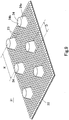
- Fig. 5 is a partially enlarged perspective view showing an antireflection film 21 according to a first embodiment of the present invention.
- Fig. 6 is a sectional view showing a section passing through the central axis of its protrusion, i.e., a protective pillar 24.
- the antireflection film 21 is formed such that, on a smooth surface of a transparent film base material 22, a large number of transparent optical projections 23 having a refractive index equal to that of the film base material 22 are densely formed.
- transparent protective pillars 24 protrusions for preventing tight contact
- transparent protective pillars 24 each having a truncated cone shape and a refractive index equal or almost equal to that of the film base material 22 are arranged at a predetermined pitch.
- the film base material 22 is made of a transparent resin having a large refractive index such as a polycarbonate resin or an acrylate resin and shaped in the form of a plate.
- the film base material 22 may be a hard resin base material or a thin flexible film base material the thickness of which is not limited to a specific value.
- Optical projections 23 are nano-sized fine projections, and have shapes such as conical shapes, truncated cone shapes, or quadrangular pyramid shape.
- the shape of the optical projection 23 may configure a part of an ellipsoid of revolution.
- the protective pillar 24 has a truncated cone shape in which the area of a distal-end surface is smaller than the area of a bottom surface, and has a height larger than that of the optical projection 23.
- the protective pillar 24 has a side surface 24a and a distal-end surface 24b.
- the distal-end surface 24b is parallel with the surface of the film base material 22.
- a solid arrow in Fig. 6 when light L2 vertically enters the antireflection film 21 in rear-surface incidence, the light L2 hitting on the side surface 24a is totally reflected by the side surface 24a, enters the distal-end surface 24b, and is totally reflected by the distal-end surface 24b.
- the light L2 enters the film base material 22 without entering the side surface 24a again and is laterally guided into the film base material 22.
- the light is regressively reflected by the protective pillar 24 and does not return in an original direction.
- the protective pillar 24 is hard to be seen due to reflected light.
- reflected light can be advantageously cut at the same level.
- a condition for causing light entering the antireflection film in rear-surface incidence to exhibit a behavior as shown in Fig. 6 will be clarified. Since light that is most easily regressively reflected is light entering an end (point a in Fig. 6 ) of the protective pillar 24, when the light cannot be regressively reflected, any light reflected by the side surface 24a is not regressively reflected.
- a condition under which light L3 entering the point a on the end of the protective pillar 24 is totally reflected by the side surface 24a is given by: 0 ° ⁇ ⁇ ⁇ arccos 1 / n
- the light L3 totally reflected by the point a enters the distal-end surface 24b
- a condition under which the light L3 is totally reflected by the distal-end surface 24b is given by: ⁇ > 0.5 ⁇ arcsin 1 / n
- a condition under which a point b is not on the side surface 24a but on the distal-end surface 24b is given by the following expression, where the diameter of the proximal-end surface of the protective pillar 24 is D, and the height of the protective pillar 24 is H, H ⁇ tan 2 ⁇ ⁇ D
- condition 3 In order to prevent regressive reflection from occurring in rear-surface incidence as described above, the conditions 3 to 6 need only be satisfied. In this case, when the angle ⁇ between the side surface 24a and the central axis comes close to 45° , the diameter D of the protective pillar 24 must be very large (see condition 6), the ⁇ must be practically smaller than 45° . For this reason, when the refractive index is a normal value, condition 3 is naturally satisfied. Furthermore, when condition 6 is satisfied, condition 5 is also satisfied. Thus, it is understood that condition 4 and condition 6 need only be satisfied. However, when all the protective pillars 24 do not satisfy condition 4, since light passes through the distal-end surface 24b and is not regressively reflected, a problem is not essentially posed. Therefore, when at least some of the protective pillars 24 satisfy condition 4, the invention of this application is useful. Consequently, it is understood that the protective pillars 24 can be prevented from shining by regressive reflection as long as condition 6 is satisfied.
- All the protective pillars 24 preferably satisfy condition 6. However, all the protective pillars 24 are not required to satisfy condition 6. When at least some of the protective pillars 24 satisfy condition 6, the effect can be obtained at a limited level.
- the angle ⁇ of the side surface 24a is desirably set to 30° or more and 40° or less, and, in particular, 30° or more and 35° or less.
- the protective pillar 24 having a height H of about 3 ⁇ m and a diameter D of 3 ⁇ m may be used.
- Fig. 7 shows micrographs obtained when light enters protective pillars having different diameters D in rear-surface incidence.
- the protective pillars are aligned in ascending order of the diameters D along the abscissa, and the protective pillars are aligned in ascending order of the intensities of reflected light along the ordinate.
- the height H of the protective pillar is set to 3 ⁇ m, and the angle ⁇ of the side surface 24a is set to 30° .
- the minimum value of the diameter D calculated on the basis of condition 6 is about 10 ⁇ m.
- the first and second pillars having the diameters D of 3 ⁇ m and 5 ⁇ m from the left are the protective pillars of the conventional technique, and the pillar having a diameter D of 10 ⁇ m is on the boundary.
- the first, second, and third protective pillars having the diameters D of 21 ⁇ m, 41 ⁇ m, and 61 ⁇ m from the right are the protective pillars according to the embodiment of the present invention.
- the protective pillars having the diameters D of 3 ⁇ m and 5 ⁇ m considerably shine due to regressive reflection.
- the protective pillar having the diameter D of 10 ⁇ m leaves regressively reflected light in relation to profile irregularity. In the protective pillar having the diameter D of 21 ⁇ m or more, regressively reflected light is rarely observed.
- Fig. 8 shows, as an example of the protective pillar, the protective pillar 24 having an elliptical section.
- H a height of a top P measured from the bottom surface of the protective pillar 24
- N1 and N2 on the surface of the protective pillar 24 at a height that is 1/2 the height H will be considered.
- a height of a horizontal plane T passing through the top P and being parallel with the bottom surface is given by H when the height is measured from the bottom surface
- points on the surface of the protective pillar 24 at the height of H/2 from the bottom surface are given by N1 and N2, respectively.
- tangent lines S1 and S2 tangent to the protective pillar surface at the points N1 and N2 on the section passing through the central axis of the protective pillar 24 are calculated, intersection points between the tangent lines S1 and S2 and the bottom surface are given by B1 and B2, respectively, and the intersection points between the tangent lines S1 and S2 and the horizontal plane T are given by C1 and C2, respectively.
- a truncated cone shape defined by a trapezoid B1 - N1 - C1 - P - C2 - N2 - B2 configured by the tangent lines S1 and S2 and the horizontal plane T that are defined by the sections as described above is a shape to which condition 6 is applied.
- a distance between B1 and B2 may be defined as the diameter D, and angles between the tangent lines S1 and S2 and the central axis may be defined as the angle ⁇ .
- FIG. 9 is a partially enlarged perspective view of the antireflection film 31 according to the second embodiment of the present invention.
- the antireflection film 31 is formed such that, on a smooth surface of a transparent film base material 22, a large number of transparent optical projections 23 having a refractive index equal to that of the film base material 22 are densely formed.
- transparent protective pillars 24 protrusions for preventing tight contact
- each having a truncated cone shape and a refractive index equal or almost equal to that of the film base material 22 are arranged at a predetermined pitch.
- the film base material 22 is made of a transparent resin having a large refractive index such as a polycarbonate resin or an acrylate resin and shaped in the form of a plate.
- the film base material 22 may be a hard resin base material or a thin flexible film base material the thickness of which is not limited to a specific value.
- Optical projections 23 are nano-sized fine projections, and have shapes such as conical shapes, truncated cone shapes, or quadrangular pyramid shape.
- the shape of the optical projection 23 may configure a part of an ellipsoid of revolution.
- the protective pillar 24 has a truncated cone shape in which the area of a distal-end surface is smaller than the area of a bottom surface, and has a height larger than that of the optical projection 23.
- the protective pillar 24 has a side surface 24a and a distal-end surface 24b.
- the distal-end surface 24b is parallel with the surface of the film base material 22.
- the protective pillar 24 has a proximal end surface having the diameter D of smaller than 60 ⁇ m. In particular, the diameter D of the protective pillar 24 is desired to be 40 ⁇ m or less in the embodiment.
- the protective pillars 24 are arranged on the film base material 22 at intervals K of 100 ⁇ m or more, preferably, 200 ⁇ m or more.
- the intervals between the protective pillars 24 are larger than those in the conventional technique.
- Fig. 11A is a photograph showing an antireflection film 14 of the conventional technique.
- Figs. 11B and 11C are photographs showing the antireflection film 31 according to the second embodiment of the present invention.
- Figs. 11A is a photograph showing an antireflection film 14 of the conventional technique.
- Figs. 11B and 11C are photographs showing the antireflection film 31 according to the second embodiment of the present invention.
- a region having a width almost equal to that of adult's finger is pressed.
- the pressed region is surrounded by a circle R.
- the pressed region is lightly colored to make it possible to discriminate the region from a peripheral region thereof .
- the color of the pressed region becomes considerably faint and blends in with a peripheral color.
- Fig. 4A shows a state in which the antireflection film 14 according to the conventional technique is partially pressed
- Fig. 4B shows a chromacity (color intensity) at a position along the antireflection film 14 in the state
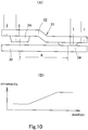
- Fig. 10A shows a state in which the antireflection film 31 according to the second embodiment of the present invention is partially pressed
- Fig. 10B shows a chromacity at a position along the antireflection film 31 in the state. Since an identification capability (resolving power) of human' s naked eye is about 100 ⁇ m, when the interval between the protective pillars 15 as shown in Fig.
- the intervals K between the protective pillars need only be 100 ⁇ m or more.
- the intervals K at which the protective pillars are arranged are desired to be 200 ⁇ m or more.
- Fig. 12A is a photograph showing an antireflection film on which protective pillars each having the diameter D of 20 ⁇ m are arranged at intervals of 200 ⁇ m.
- Fig. 12B is a photograph showing an antireflection film on which protective pillars each having the diameter D of 40 ⁇ m are arranged at intervals of 200 ⁇ m.
- Fig. 12C is a photograph showing an antireflection film on which protective pillars each having the diameter D of 60 ⁇ m are arranged at intervals of 200 ⁇ m.
- the protective pillars have the diameters D of 60 ⁇ m, as shown in Fig. 12C , feeling of pimples caused by the protective pillars becomes considerably conspicuous.
- the diameters D of the protective pillars 24 are desired to be smaller than 60 ⁇ m.
- the protective pillars 24 having the diameters D of 40 ⁇ m or less become hardly conspicuous.
- the protective pillars 24 are desirably arranged at the intervals K of 100 ⁇ m or more and desirably have the diameters D of smaller than 60 ⁇ m.
- the intervals K between the protective pillars 24 are desired to be, in particular, 200 ⁇ m or more.
- the diameters D of the protective pillars 24 are preferably minimized as long as the strengths of the protective pillars 24 can be kept. In particular, the diameters D are desired to be 40 ⁇ m or less.
- the protective pillars 24 preferably have an area density (percentage of a total area of protective pillars included in a certain area on a film base material) of almost 1%.
- FIGs. 13A to 13C show some modes of a display device to which an antireflection film 40 (for example, the antireflection film 21 or the antireflection film 31) according to the present invention is stuck.
- a display device 41 shown in Fig. 13A is obtained by superposing a cover panel 43 on the front surface of the image display panel 42 such as a liquid crystal display panel (LCD) or an organic EL (OLED) through an air gap (space).
- the antireflection film 40 is stuck to each of the rear surface of the cover panel 43 and the front surface of the image display panel 42.
- the antireflection films 40 are stuck to the front surface and the rear surface of the cover panel 43 and the front surface of the image display panel 42, respectively.
- the antireflection film 40 is also stuck to the front surface of the cover panel 43 as shown in Fig. 13B to increase an antireflection effect.
- the antireflection film 40 on the front surface of the cover panel 43 is touched by a user, the antireflection film 40 may be damaged or contaminated.
- the antireflection film 40 is stuck to only one of the rear surface of the cover panel 43 and the front surface of the image display panel 42. In the mode as shown in Fig. 13C , an antireflection effect is deteriorated. However, since the cost also decreases, the mode is useful depending on applications.
- the image display panel 42 may be for a monochrome display or a color display.
- the cover panel 43 is a protective sheet made of a transparent resin and having a uniform thickness.
- an alignment pitch of the protective pillars 24 on the antireflection film 40 may be almost equal to a pixel pitch of the image display panel 42.
- the alignment pitch of the protective pillars 24 is almost equal to the pixel pitch, Moire fringes may occur on the screen of the display device.
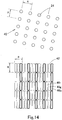
- the antireflection film 40 is rotated by about 90° with reference to the image display panel 42, so that a protective pillar alignment direction of the pitch p on the antireflection film 40 is almost parallel with a pixel alignment direction of the pitch q on the image display panel 42, and a protective pillar alignment direction of the pitch q on the antireflection film 40 is almost parallel with a pixel alignment direction of the pitch p on the image display panel 42.
- a protective pillar alignment direction of the pitch p on the antireflection film 40 is almost parallel with a pixel alignment direction of the pitch q on the image display panel 42.
- the alignment directions of the protective pillars 24 need only be used to be slightly inclined with reference to the alignment directions of the pixels such that the alignment directions of the protective pillars 24 at the different pitches p and q are not parallel with the pixel alignment directions.
- one set of a red pixel 46r, a green pixel 46g, and a blue pixel 46b configures one pixel.
- interference fringes (Newton's ring) occur when the cover panel 43 is pressed to make a gap between the cover panel 43 and the image display panel 42 about 60 ⁇ m.
- Fig. 16A shows a state in which the cover panel 43 is pressed with a finger to generate interference fringes.
- interference fringes do not occur unless the gap is about 2 ⁇ m.
- Fig. 16B shows a structure in which the antireflection film 40 having the protective pillars 24 each having a height of 3 ⁇ m is stuck to the rear surface of the cover panel 43.
- Fig. 16B is also a photograph obtained when the antireflection film 40 is pressed with a finger as in Fig. 16A . In this photograph, interference fringes do not occur.
- the protective pillars 24 each having a height of 2 ⁇ m or more, more preferably, about 3 ⁇ m are advantageously arranged on the antireflection film 40.
- the protective pillars 24 are advantageously arranged at a density of 1% or more per unit area.
- an intermediate area between the protective pillar 24 and the protective pillar 24 may be disadvantageously brought into tight contact with the image display panel 42.
Landscapes
- Physics & Mathematics (AREA)
- Nonlinear Science (AREA)
- General Physics & Mathematics (AREA)
- Optics & Photonics (AREA)
- Mathematical Physics (AREA)
- Chemical & Material Sciences (AREA)
- Crystallography & Structural Chemistry (AREA)
- Liquid Crystal (AREA)
- Devices For Indicating Variable Information By Combining Individual Elements (AREA)
- Surface Treatment Of Optical Elements (AREA)
Claims (8)
- Antireflexionsionsfolie (21, 31, 40), die Folgendes umfasst:ein Foliengrundmaterial (22),eine Antireflexionsstruktur, die von einer Vielzahl feiner optischer Vorsprünge (23) gebildet wird, welche auf einer Oberfläche des Foliengrundmaterials (22) ausgebildet sind, undeine Vielzahl Vorsprünge (24), die neben feinen optischen Vorsprüngen (23) der Vielzahl feiner optischer Vorsprünge (23) auf der Oberfläche des Foliengrundmaterials (22) ausgebildet sind, wobei jeder Vorsprung (24) eine Kegelstumpfform mit einer distalen Stirnfläche (24b) und eine von der distalen Stirnfläche (24b) definierte Höhe (H) aufweist, die größer ist als die des optischen Vorsprungs (23), wobei sich bei jedem der Vielzahl Vorsprünge (24) eine Querschnittsfläche eines parallel zur Oberfläche des Foliengrundmaterials (22) verlaufenden Querschnitts von einem proximalen Endabschnitt aus hin zur distalen Stirnfläche (24b) allmählich verkleinert und,wenn ein Durchmesser des Vorsprungs (24) an dessen proximalen Ende, eine Höhe des Vorsprungs (24) und ein Winkel zwischen einer Seitenfläche (24a) des Vorsprungs (24) und einer Mittelachse des Vorsprungs (24) an einem durch die Mittelachse des Vorsprungs (24) verlaufenden Abschnitt durch D, H und θ gegeben ist, die Antireflexionsfolie (21, 31, 40) folgende Beziehung aufweist:

wenn ein Brechungsindex des Vorsprungs (24) durch n gegeben ist, mindestens ein Vorsprung (24) der Vielzahl von Vorsprüngen (24) der folgenden Beziehung genügt:
- Antireflexionsfolie nach Anspruch 1, wobei eine Abmessung jedes der Vorsprünge (24) bei Betrachtung von oben her weniger als 60 µm beträgt und die Vorsprünge (24) in Abständen (K) von 100 µm oder mehr angeordnet sind.
- Antireflexionsfolie nach Anspruch 2, wobei die Abmessung (D) jedes der Vorsprünge (24) bei Betrachtung von oben her 40 µm oder weniger beträgt.
- Antireflexionsfolie nach Anspruch 2, wobei ein Abstand (K) zwischen den Vorsprüngen (24) 200 µm oder mehr beträgt.
- Antireflexionsfolie nach Anspruch 1 oder 2, wobei eine Höhe (H) jedes der Vorsprünge (24) 2 µm oder mehr beträgt.
- Antireflexionsfolie nach Anspruch 5, wobei eine Dichte des Vorsprungs (24) pro Flächeneinheit 1% oder mehr beträgt.
- Anzeigevorrichtung, die Folgendes umfasst:die Antireflexionsfolie nach Anspruch 1 oder 2 undeinen Flüssigkristallbildschirm (42),wobei die Antireflexionsfolie so auf den Flüssigkristallbildschirm (42) gelegt ist, dass eine Ausrichtrichtung der Vorsprünge (24) in Bezug zu einer Ausrichtrichtung des Flüssigkristallbildschirms (42) schräg ist.
- Anzeige, die Folgendes umfasst:die Antireflexionsfolie nach Anspruch 1 oder 2,ein Informationsanzeigemodul (41, 44, 45) undeine Abdeckplatte (43) oder einBerührungsbildschirmmodul,wobei die Antireflexionsfolie zwischen dem Informationsanzeigemodul (41, 44, 45) und der Abdeckplatte (43) oder dem Berührungsbildschirmmodul angeordnet ist.
Applications Claiming Priority (3)
| Application Number | Priority Date | Filing Date | Title |
|---|---|---|---|
| JP2012059487A JP5931524B2 (ja) | 2012-03-15 | 2012-03-15 | 反射防止フィルム |
| JP2012059453A JP6016394B2 (ja) | 2012-03-15 | 2012-03-15 | 反射防止フィルムを備えた情報表示装置 |
| PCT/JP2013/056806 WO2013137251A1 (ja) | 2012-03-15 | 2013-03-12 | 反射防止フィルム |
Publications (3)
| Publication Number | Publication Date |
|---|---|
| EP2827177A1 EP2827177A1 (de) | 2015-01-21 |
| EP2827177A4 EP2827177A4 (de) | 2015-11-04 |
| EP2827177B1 true EP2827177B1 (de) | 2017-11-29 |
Family
ID=49161157
Family Applications (1)
| Application Number | Title | Priority Date | Filing Date |
|---|---|---|---|
| EP13760782.6A Not-in-force EP2827177B1 (de) | 2012-03-15 | 2013-03-12 | Antireflexionsfolie |
Country Status (8)
| Country | Link |
|---|---|
| US (1) | US20150116834A1 (de) |
| EP (1) | EP2827177B1 (de) |
| KR (1) | KR101852659B1 (de) |
| CN (1) | CN104169746B (de) |
| DK (1) | DK2827177T3 (de) |
| SG (1) | SG11201405513QA (de) |
| TW (1) | TWI572885B (de) |
| WO (1) | WO2013137251A1 (de) |
Families Citing this family (7)
| Publication number | Priority date | Publication date | Assignee | Title |
|---|---|---|---|---|
| GB2527271A (en) * | 2014-04-07 | 2015-12-23 | Ujett D P Ltd | Coated optical substrates |
| US9851474B2 (en) * | 2014-07-10 | 2017-12-26 | Scivax Corporation | Optical component and method of producing the same |
| DE102015122768A1 (de) * | 2015-12-23 | 2017-06-29 | Temicon Gmbh | Plattenförmiges optisches Element zur Auskopplung von Licht |
| US20180188861A1 (en) * | 2017-01-03 | 2018-07-05 | Innolux Corporation | Display device |
| US10527878B2 (en) * | 2017-09-13 | 2020-01-07 | Int Tech Co., Ltd. | Display panel and method for manufacturing the same |
| US10804347B2 (en) * | 2017-09-13 | 2020-10-13 | Int Tech Co., Ltd. | Display panel |
| CN111766649A (zh) * | 2019-03-30 | 2020-10-13 | 华为技术有限公司 | 一种光学元件、摄像头模组、终端和光学元件的加工方法 |
Citations (1)
| Publication number | Priority date | Publication date | Assignee | Title |
|---|---|---|---|---|
| EP2746824A1 (de) * | 2011-09-15 | 2014-06-25 | Soken Chemical & Engineering Co., Ltd. | Kontaktverhinderungsfilm, berührungsbildschirm und abdeckplatte für eine anzeigevorrichtung |
Family Cites Families (23)
| Publication number | Priority date | Publication date | Assignee | Title |
|---|---|---|---|---|
| JP4168179B2 (ja) * | 1995-03-03 | 2008-10-22 | スリーエム カンパニー | 種々の高さの構造化面を有する光指向性フィルム及び該フィルムから作製された光指向性製品 |
| JP3358935B2 (ja) * | 1995-10-02 | 2002-12-24 | シャープ株式会社 | 液晶表示素子およびその製造方法 |
| TW589504B (en) * | 1997-06-12 | 2004-06-01 | Sharp Kk | Liquid crystal display device |
| TW459275B (en) * | 1999-07-06 | 2001-10-11 | Semiconductor Energy Lab | Semiconductor device and method of fabricating the same |
| JP2002122702A (ja) | 2000-10-17 | 2002-04-26 | Matsushita Electric Ind Co Ltd | 光学フィルム、及び表示素子 |
| JP2003279705A (ja) * | 2002-03-25 | 2003-10-02 | Sanyo Electric Co Ltd | 反射防止部材 |
| JP4262944B2 (ja) | 2002-08-08 | 2009-05-13 | アルプス電気株式会社 | 照明装置および液晶表示装置 |
| JP2004177806A (ja) * | 2002-11-28 | 2004-06-24 | Alps Electric Co Ltd | 反射防止構造および照明装置と液晶表示装置並びに反射防止膜成型用金型 |
| JP4225110B2 (ja) * | 2003-05-09 | 2009-02-18 | コニカミノルタオプト株式会社 | 防眩性反射防止フィルムとその製造方法、及びそれを用いた偏光板と表示装置 |
| US7384173B2 (en) * | 2004-12-30 | 2008-06-10 | 3M Innovative Properties Company | Brightness enhancement article |
| JP2006331757A (ja) * | 2005-05-25 | 2006-12-07 | Omron Corp | 面光源装置と該面光源装置を用いた画像表示装置及び電子機器 |
| JP2007178873A (ja) * | 2005-12-28 | 2007-07-12 | Nikon Corp | 光学素子 |
| EP2038684B1 (de) | 2006-05-31 | 2016-03-16 | Semiconductor Energy Laboratory Co., Ltd. | Anzeigeeinrichtung |
| US20080049330A1 (en) * | 2006-08-25 | 2008-02-28 | 3M Innovative Properties Company | Light directing laminate |
| JP2009009078A (ja) | 2007-05-31 | 2009-01-15 | Dainippon Printing Co Ltd | 光学部材、面光源装置および液晶表示装置 |
| JP4539759B2 (ja) | 2007-10-01 | 2010-09-08 | オムロン株式会社 | 反射防止シート、表示素子及びディスプレイ装置 |
| JP2009150981A (ja) | 2007-12-19 | 2009-07-09 | Toppan Printing Co Ltd | 光学シート、バックライトユニット及びディスプレイ装置 |
| JP5254664B2 (ja) * | 2008-05-27 | 2013-08-07 | 株式会社Dnpファインケミカル | 反射防止膜及びその製造方法 |
| JP4968953B2 (ja) * | 2008-11-17 | 2012-07-04 | 修司 岩田 | 反射防止機能を有する機能性基板とその製造方法 |
| JP5257066B2 (ja) * | 2008-12-26 | 2013-08-07 | ソニー株式会社 | 光学素子、表示装置、反射防止機能付き光学部品、および原盤 |
| JP4626721B1 (ja) | 2009-09-02 | 2011-02-09 | ソニー株式会社 | 透明導電性電極、タッチパネル、情報入力装置、および表示装置 |
| JP2011107195A (ja) * | 2009-11-12 | 2011-06-02 | Olympus Corp | 光学素子および光学素子の製造方法ならびに微細凹凸構造および成形型 |
| JP2012037622A (ja) * | 2010-08-04 | 2012-02-23 | Dainippon Printing Co Ltd | 光学シート、面光源装置および透過型表示装置 |
-
2013
- 2013-03-12 EP EP13760782.6A patent/EP2827177B1/de not_active Not-in-force
- 2013-03-12 SG SG11201405513QA patent/SG11201405513QA/en unknown
- 2013-03-12 US US14/390,606 patent/US20150116834A1/en not_active Abandoned
- 2013-03-12 DK DK13760782.6T patent/DK2827177T3/en active
- 2013-03-12 CN CN201380014256.1A patent/CN104169746B/zh not_active Expired - Fee Related
- 2013-03-12 WO PCT/JP2013/056806 patent/WO2013137251A1/ja not_active Ceased
- 2013-03-12 KR KR1020147023836A patent/KR101852659B1/ko not_active Expired - Fee Related
- 2013-03-14 TW TW102109111A patent/TWI572885B/zh not_active IP Right Cessation
Patent Citations (1)
| Publication number | Priority date | Publication date | Assignee | Title |
|---|---|---|---|---|
| EP2746824A1 (de) * | 2011-09-15 | 2014-06-25 | Soken Chemical & Engineering Co., Ltd. | Kontaktverhinderungsfilm, berührungsbildschirm und abdeckplatte für eine anzeigevorrichtung |
Also Published As
| Publication number | Publication date |
|---|---|
| TW201344233A (zh) | 2013-11-01 |
| EP2827177A1 (de) | 2015-01-21 |
| CN104169746B (zh) | 2016-06-08 |
| US20150116834A1 (en) | 2015-04-30 |
| KR101852659B1 (ko) | 2018-04-26 |
| DK2827177T3 (en) | 2018-02-12 |
| WO2013137251A1 (ja) | 2013-09-19 |
| SG11201405513QA (en) | 2014-11-27 |
| EP2827177A4 (de) | 2015-11-04 |
| TWI572885B (zh) | 2017-03-01 |
| KR20150009515A (ko) | 2015-01-26 |
| CN104169746A (zh) | 2014-11-26 |
Similar Documents
| Publication | Publication Date | Title |
|---|---|---|
| EP2827177B1 (de) | Antireflexionsfolie | |
| CN109358447B (zh) | 光学膜及具有光学膜的显示装置 | |
| KR100487105B1 (ko) | 광학필름 | |
| EP2728570A1 (de) | Anzeigevorrichtung vom Array-Typ | |
| US20140063414A1 (en) | Backlight unit and liquid crystal display device using the same | |
| EP1746457B1 (de) | Lichtquelle mit Lichtleiter, welcher lichtstreuende und lichtlenkende Strukturen aufweist | |
| US9557448B2 (en) | Contact prevention film, touch panel and display device cover panel | |
| US9261637B2 (en) | Surface light source device and its light guide plate | |
| CN110865741B (zh) | 一种触控显示模组及显示装置 | |
| JPH10301110A (ja) | 画像表示装置 | |
| KR102578465B1 (ko) | 표시 장치 | |
| JP2003058071A (ja) | 遮光透明シートおよび遮光画面装置 | |
| JP2007047545A (ja) | 液晶表示装置、面光源装置及び情報機器 | |
| WO2012005135A1 (ja) | 光拡散シートおよび当該光拡散シートを備えた表示装置 | |
| JP2016020996A (ja) | タイリングパネル | |
| CN110531553B (zh) | 一种背光模组、其制作方法及显示装置 | |
| JP6016394B2 (ja) | 反射防止フィルムを備えた情報表示装置 | |
| JP5931524B2 (ja) | 反射防止フィルム | |
| US20100189962A1 (en) | Transparent coordinate input device and transparent composite material having ridge portion formed in transparent resistance film | |
| KR101054037B1 (ko) | 백라이트 유닛용 광학시트 | |
| JP4164407B2 (ja) | 透明座標入力装置および透明複合材 | |
| JP6957869B2 (ja) | 表示装置 | |
| JP6812713B2 (ja) | 配列型表示装置 | |
| JP2008191176A (ja) | 光出射角制限シート |
Legal Events
| Date | Code | Title | Description |
|---|---|---|---|
| PUAI | Public reference made under article 153(3) epc to a published international application that has entered the european phase |
Free format text: ORIGINAL CODE: 0009012 |
|
| 17P | Request for examination filed |
Effective date: 20141002 |
|
| AK | Designated contracting states |
Kind code of ref document: A1 Designated state(s): AL AT BE BG CH CY CZ DE DK EE ES FI FR GB GR HR HU IE IS IT LI LT LU LV MC MK MT NL NO PL PT RO RS SE SI SK SM TR |
|
| AX | Request for extension of the european patent |
Extension state: BA ME |
|
| DAX | Request for extension of the european patent (deleted) | ||
| RA4 | Supplementary search report drawn up and despatched (corrected) |
Effective date: 20151007 |
|
| RIC1 | Information provided on ipc code assigned before grant |
Ipc: G02B 1/11 20150101AFI20151001BHEP Ipc: G02F 1/1335 20060101ALI20151001BHEP Ipc: G02B 1/118 20150101ALI20151001BHEP |
|
| 17Q | First examination report despatched |
Effective date: 20160921 |
|
| STAA | Information on the status of an ep patent application or granted ep patent |
Free format text: STATUS: EXAMINATION IS IN PROGRESS |
|
| GRAP | Despatch of communication of intention to grant a patent |
Free format text: ORIGINAL CODE: EPIDOSNIGR1 |
|
| STAA | Information on the status of an ep patent application or granted ep patent |
Free format text: STATUS: GRANT OF PATENT IS INTENDED |
|
| INTG | Intention to grant announced |
Effective date: 20170612 |
|
| GRAS | Grant fee paid |
Free format text: ORIGINAL CODE: EPIDOSNIGR3 |
|
| GRAA | (expected) grant |
Free format text: ORIGINAL CODE: 0009210 |
|
| STAA | Information on the status of an ep patent application or granted ep patent |
Free format text: STATUS: THE PATENT HAS BEEN GRANTED |
|
| AK | Designated contracting states |
Kind code of ref document: B1 Designated state(s): AL AT BE BG CH CY CZ DE DK EE ES FI FR GB GR HR HU IE IS IT LI LT LU LV MC MK MT NL NO PL PT RO RS SE SI SK SM TR |
|
| REG | Reference to a national code |
Ref country code: CH Ref legal event code: EP |
|
| REG | Reference to a national code |
Ref country code: AT Ref legal event code: REF Ref document number: 950899 Country of ref document: AT Kind code of ref document: T Effective date: 20171215 |
|
| REG | Reference to a national code |
Ref country code: IE Ref legal event code: FG4D |
|
| REG | Reference to a national code |
Ref country code: DE Ref legal event code: R096 Ref document number: 602013030113 Country of ref document: DE |
|
| REG | Reference to a national code |
Ref country code: DK Ref legal event code: T3 Effective date: 20180207 |
|
| REG | Reference to a national code |
Ref country code: FR Ref legal event code: PLFP Year of fee payment: 6 |
|
| REG | Reference to a national code |
Ref country code: NL Ref legal event code: MP Effective date: 20171129 |
|
| REG | Reference to a national code |
Ref country code: LT Ref legal event code: MG4D |
|
| PG25 | Lapsed in a contracting state [announced via postgrant information from national office to epo] |
Ref country code: NO Free format text: LAPSE BECAUSE OF FAILURE TO SUBMIT A TRANSLATION OF THE DESCRIPTION OR TO PAY THE FEE WITHIN THE PRESCRIBED TIME-LIMIT Effective date: 20180228 Ref country code: ES Free format text: LAPSE BECAUSE OF FAILURE TO SUBMIT A TRANSLATION OF THE DESCRIPTION OR TO PAY THE FEE WITHIN THE PRESCRIBED TIME-LIMIT Effective date: 20171129 Ref country code: FI Free format text: LAPSE BECAUSE OF FAILURE TO SUBMIT A TRANSLATION OF THE DESCRIPTION OR TO PAY THE FEE WITHIN THE PRESCRIBED TIME-LIMIT Effective date: 20171129 Ref country code: LT Free format text: LAPSE BECAUSE OF FAILURE TO SUBMIT A TRANSLATION OF THE DESCRIPTION OR TO PAY THE FEE WITHIN THE PRESCRIBED TIME-LIMIT Effective date: 20171129 Ref country code: SE Free format text: LAPSE BECAUSE OF FAILURE TO SUBMIT A TRANSLATION OF THE DESCRIPTION OR TO PAY THE FEE WITHIN THE PRESCRIBED TIME-LIMIT Effective date: 20171129 |
|
| PG25 | Lapsed in a contracting state [announced via postgrant information from national office to epo] |
Ref country code: LV Free format text: LAPSE BECAUSE OF FAILURE TO SUBMIT A TRANSLATION OF THE DESCRIPTION OR TO PAY THE FEE WITHIN THE PRESCRIBED TIME-LIMIT Effective date: 20171129 Ref country code: RS Free format text: LAPSE BECAUSE OF FAILURE TO SUBMIT A TRANSLATION OF THE DESCRIPTION OR TO PAY THE FEE WITHIN THE PRESCRIBED TIME-LIMIT Effective date: 20171129 Ref country code: HR Free format text: LAPSE BECAUSE OF FAILURE TO SUBMIT A TRANSLATION OF THE DESCRIPTION OR TO PAY THE FEE WITHIN THE PRESCRIBED TIME-LIMIT Effective date: 20171129 Ref country code: BG Free format text: LAPSE BECAUSE OF FAILURE TO SUBMIT A TRANSLATION OF THE DESCRIPTION OR TO PAY THE FEE WITHIN THE PRESCRIBED TIME-LIMIT Effective date: 20180228 Ref country code: GR Free format text: LAPSE BECAUSE OF FAILURE TO SUBMIT A TRANSLATION OF THE DESCRIPTION OR TO PAY THE FEE WITHIN THE PRESCRIBED TIME-LIMIT Effective date: 20180301 |
|
| PG25 | Lapsed in a contracting state [announced via postgrant information from national office to epo] |
Ref country code: NL Free format text: LAPSE BECAUSE OF FAILURE TO SUBMIT A TRANSLATION OF THE DESCRIPTION OR TO PAY THE FEE WITHIN THE PRESCRIBED TIME-LIMIT Effective date: 20171129 |
|
| PG25 | Lapsed in a contracting state [announced via postgrant information from national office to epo] |
Ref country code: CY Free format text: LAPSE BECAUSE OF FAILURE TO SUBMIT A TRANSLATION OF THE DESCRIPTION OR TO PAY THE FEE WITHIN THE PRESCRIBED TIME-LIMIT Effective date: 20171129 Ref country code: EE Free format text: LAPSE BECAUSE OF FAILURE TO SUBMIT A TRANSLATION OF THE DESCRIPTION OR TO PAY THE FEE WITHIN THE PRESCRIBED TIME-LIMIT Effective date: 20171129 Ref country code: SK Free format text: LAPSE BECAUSE OF FAILURE TO SUBMIT A TRANSLATION OF THE DESCRIPTION OR TO PAY THE FEE WITHIN THE PRESCRIBED TIME-LIMIT Effective date: 20171129 Ref country code: CZ Free format text: LAPSE BECAUSE OF FAILURE TO SUBMIT A TRANSLATION OF THE DESCRIPTION OR TO PAY THE FEE WITHIN THE PRESCRIBED TIME-LIMIT Effective date: 20171129 |
|
| REG | Reference to a national code |
Ref country code: DE Ref legal event code: R097 Ref document number: 602013030113 Country of ref document: DE |
|
| PG25 | Lapsed in a contracting state [announced via postgrant information from national office to epo] |
Ref country code: PL Free format text: LAPSE BECAUSE OF FAILURE TO SUBMIT A TRANSLATION OF THE DESCRIPTION OR TO PAY THE FEE WITHIN THE PRESCRIBED TIME-LIMIT Effective date: 20171129 Ref country code: SM Free format text: LAPSE BECAUSE OF FAILURE TO SUBMIT A TRANSLATION OF THE DESCRIPTION OR TO PAY THE FEE WITHIN THE PRESCRIBED TIME-LIMIT Effective date: 20171129 Ref country code: IT Free format text: LAPSE BECAUSE OF FAILURE TO SUBMIT A TRANSLATION OF THE DESCRIPTION OR TO PAY THE FEE WITHIN THE PRESCRIBED TIME-LIMIT Effective date: 20171129 Ref country code: RO Free format text: LAPSE BECAUSE OF FAILURE TO SUBMIT A TRANSLATION OF THE DESCRIPTION OR TO PAY THE FEE WITHIN THE PRESCRIBED TIME-LIMIT Effective date: 20171129 |
|
| PLBE | No opposition filed within time limit |
Free format text: ORIGINAL CODE: 0009261 |
|
| STAA | Information on the status of an ep patent application or granted ep patent |
Free format text: STATUS: NO OPPOSITION FILED WITHIN TIME LIMIT |
|
| REG | Reference to a national code |
Ref country code: CH Ref legal event code: PL |
|
| 26N | No opposition filed |
Effective date: 20180830 |
|
| GBPC | Gb: european patent ceased through non-payment of renewal fee |
Effective date: 20180312 |
|
| PG25 | Lapsed in a contracting state [announced via postgrant information from national office to epo] |
Ref country code: SI Free format text: LAPSE BECAUSE OF FAILURE TO SUBMIT A TRANSLATION OF THE DESCRIPTION OR TO PAY THE FEE WITHIN THE PRESCRIBED TIME-LIMIT Effective date: 20171129 Ref country code: MC Free format text: LAPSE BECAUSE OF FAILURE TO SUBMIT A TRANSLATION OF THE DESCRIPTION OR TO PAY THE FEE WITHIN THE PRESCRIBED TIME-LIMIT Effective date: 20171129 |
|
| REG | Reference to a national code |
Ref country code: BE Ref legal event code: MM Effective date: 20180331 |
|
| REG | Reference to a national code |
Ref country code: IE Ref legal event code: MM4A |
|
| PG25 | Lapsed in a contracting state [announced via postgrant information from national office to epo] |
Ref country code: LU Free format text: LAPSE BECAUSE OF NON-PAYMENT OF DUE FEES Effective date: 20180312 |
|
| PG25 | Lapsed in a contracting state [announced via postgrant information from national office to epo] |
Ref country code: IE Free format text: LAPSE BECAUSE OF NON-PAYMENT OF DUE FEES Effective date: 20180312 |
|
| PG25 | Lapsed in a contracting state [announced via postgrant information from national office to epo] |
Ref country code: BE Free format text: LAPSE BECAUSE OF NON-PAYMENT OF DUE FEES Effective date: 20180331 Ref country code: GB Free format text: LAPSE BECAUSE OF NON-PAYMENT OF DUE FEES Effective date: 20180312 Ref country code: CH Free format text: LAPSE BECAUSE OF NON-PAYMENT OF DUE FEES Effective date: 20180331 Ref country code: LI Free format text: LAPSE BECAUSE OF NON-PAYMENT OF DUE FEES Effective date: 20180331 |
|
| PGFP | Annual fee paid to national office [announced via postgrant information from national office to epo] |
Ref country code: DE Payment date: 20190321 Year of fee payment: 7 Ref country code: FR Payment date: 20190322 Year of fee payment: 7 |
|
| PGFP | Annual fee paid to national office [announced via postgrant information from national office to epo] |
Ref country code: DK Payment date: 20190322 Year of fee payment: 7 Ref country code: AT Payment date: 20190321 Year of fee payment: 7 |
|
| PG25 | Lapsed in a contracting state [announced via postgrant information from national office to epo] |
Ref country code: MT Free format text: LAPSE BECAUSE OF NON-PAYMENT OF DUE FEES Effective date: 20180312 |
|
| PG25 | Lapsed in a contracting state [announced via postgrant information from national office to epo] |
Ref country code: TR Free format text: LAPSE BECAUSE OF FAILURE TO SUBMIT A TRANSLATION OF THE DESCRIPTION OR TO PAY THE FEE WITHIN THE PRESCRIBED TIME-LIMIT Effective date: 20171129 |
|
| PG25 | Lapsed in a contracting state [announced via postgrant information from national office to epo] |
Ref country code: HU Free format text: LAPSE BECAUSE OF FAILURE TO SUBMIT A TRANSLATION OF THE DESCRIPTION OR TO PAY THE FEE WITHIN THE PRESCRIBED TIME-LIMIT; INVALID AB INITIO Effective date: 20130312 Ref country code: PT Free format text: LAPSE BECAUSE OF FAILURE TO SUBMIT A TRANSLATION OF THE DESCRIPTION OR TO PAY THE FEE WITHIN THE PRESCRIBED TIME-LIMIT Effective date: 20171129 |
|
| PG25 | Lapsed in a contracting state [announced via postgrant information from national office to epo] |
Ref country code: MK Free format text: LAPSE BECAUSE OF NON-PAYMENT OF DUE FEES Effective date: 20171129 |
|
| PG25 | Lapsed in a contracting state [announced via postgrant information from national office to epo] |
Ref country code: AL Free format text: LAPSE BECAUSE OF FAILURE TO SUBMIT A TRANSLATION OF THE DESCRIPTION OR TO PAY THE FEE WITHIN THE PRESCRIBED TIME-LIMIT Effective date: 20171129 Ref country code: IS Free format text: LAPSE BECAUSE OF FAILURE TO SUBMIT A TRANSLATION OF THE DESCRIPTION OR TO PAY THE FEE WITHIN THE PRESCRIBED TIME-LIMIT Effective date: 20180329 |
|
| REG | Reference to a national code |
Ref country code: DE Ref legal event code: R119 Ref document number: 602013030113 Country of ref document: DE |
|
| REG | Reference to a national code |
Ref country code: DK Ref legal event code: EBP Effective date: 20200331 |
|
| REG | Reference to a national code |
Ref country code: AT Ref legal event code: MM01 Ref document number: 950899 Country of ref document: AT Kind code of ref document: T Effective date: 20200312 |
|
| PG25 | Lapsed in a contracting state [announced via postgrant information from national office to epo] |
Ref country code: AT Free format text: LAPSE BECAUSE OF NON-PAYMENT OF DUE FEES Effective date: 20200312 Ref country code: FR Free format text: LAPSE BECAUSE OF NON-PAYMENT OF DUE FEES Effective date: 20200331 Ref country code: DE Free format text: LAPSE BECAUSE OF NON-PAYMENT OF DUE FEES Effective date: 20201001 |
|
| PG25 | Lapsed in a contracting state [announced via postgrant information from national office to epo] |
Ref country code: DK Free format text: LAPSE BECAUSE OF NON-PAYMENT OF DUE FEES Effective date: 20200331 |
|
| REG | Reference to a national code |
Ref country code: AT Ref legal event code: UEP Ref document number: 950899 Country of ref document: AT Kind code of ref document: T Effective date: 20171129 |