EP2828802B1 - Rfid-transponder - Google Patents
Rfid-transponder Download PDFInfo
- Publication number
- EP2828802B1 EP2828802B1 EP13718101.2A EP13718101A EP2828802B1 EP 2828802 B1 EP2828802 B1 EP 2828802B1 EP 13718101 A EP13718101 A EP 13718101A EP 2828802 B1 EP2828802 B1 EP 2828802B1
- Authority
- EP
- European Patent Office
- Prior art keywords
- rfid transponder
- metallization
- antenna
- carrier
- carrier member
- Prior art date
- Legal status (The legal status is an assumption and is not a legal conclusion. Google has not performed a legal analysis and makes no representation as to the accuracy of the status listed.)
- Not-in-force
Links
Images


Classifications
-
- G—PHYSICS
- G06—COMPUTING OR CALCULATING; COUNTING
- G06K—GRAPHICAL DATA READING; PRESENTATION OF DATA; RECORD CARRIERS; HANDLING RECORD CARRIERS
- G06K19/00—Record carriers for use with machines and with at least a part designed to carry digital markings
- G06K19/06—Record carriers for use with machines and with at least a part designed to carry digital markings characterised by the kind of the digital marking, e.g. shape, nature, code
- G06K19/067—Record carriers with conductive marks, printed circuits or semiconductor circuit elements, e.g. credit or identity cards also with resonating or responding marks without active components
- G06K19/07—Record carriers with conductive marks, printed circuits or semiconductor circuit elements, e.g. credit or identity cards also with resonating or responding marks without active components with integrated circuit chips
- G06K19/077—Constructional details, e.g. mounting of circuits in the carrier
- G06K19/07749—Constructional details, e.g. mounting of circuits in the carrier the record carrier being capable of non-contact communication, e.g. constructional details of the antenna of a non-contact smart card
- G06K19/07771—Constructional details, e.g. mounting of circuits in the carrier the record carrier being capable of non-contact communication, e.g. constructional details of the antenna of a non-contact smart card the record carrier comprising means for minimising adverse effects on the data communication capability of the record carrier, e.g. minimising Eddy currents induced in a proximate metal or otherwise electromagnetically interfering object
-
- G—PHYSICS
- G06—COMPUTING OR CALCULATING; COUNTING
- G06K—GRAPHICAL DATA READING; PRESENTATION OF DATA; RECORD CARRIERS; HANDLING RECORD CARRIERS
- G06K19/00—Record carriers for use with machines and with at least a part designed to carry digital markings
- G06K19/06—Record carriers for use with machines and with at least a part designed to carry digital markings characterised by the kind of the digital marking, e.g. shape, nature, code
- G06K19/067—Record carriers with conductive marks, printed circuits or semiconductor circuit elements, e.g. credit or identity cards also with resonating or responding marks without active components
- G06K19/07—Record carriers with conductive marks, printed circuits or semiconductor circuit elements, e.g. credit or identity cards also with resonating or responding marks without active components with integrated circuit chips
- G06K19/077—Constructional details, e.g. mounting of circuits in the carrier
- G06K19/07749—Constructional details, e.g. mounting of circuits in the carrier the record carrier being capable of non-contact communication, e.g. constructional details of the antenna of a non-contact smart card
- G06K19/07773—Antenna details
- G06K19/07786—Antenna details the antenna being of the HF type, such as a dipole
-
- G—PHYSICS
- G06—COMPUTING OR CALCULATING; COUNTING
- G06K—GRAPHICAL DATA READING; PRESENTATION OF DATA; RECORD CARRIERS; HANDLING RECORD CARRIERS
- G06K19/00—Record carriers for use with machines and with at least a part designed to carry digital markings
- G06K19/06—Record carriers for use with machines and with at least a part designed to carry digital markings characterised by the kind of the digital marking, e.g. shape, nature, code
- G06K19/067—Record carriers with conductive marks, printed circuits or semiconductor circuit elements, e.g. credit or identity cards also with resonating or responding marks without active components
- G06K19/07—Record carriers with conductive marks, printed circuits or semiconductor circuit elements, e.g. credit or identity cards also with resonating or responding marks without active components with integrated circuit chips
- G06K19/077—Constructional details, e.g. mounting of circuits in the carrier
- G06K19/07749—Constructional details, e.g. mounting of circuits in the carrier the record carrier being capable of non-contact communication, e.g. constructional details of the antenna of a non-contact smart card
- G06K19/07773—Antenna details
- G06K19/07792—Antenna details the antenna adapted for extending in three dimensions
-
- H—ELECTRICITY
- H01—ELECTRIC ELEMENTS
- H01Q—ANTENNAS, i.e. RADIO AERIALS
- H01Q1/00—Details of, or arrangements associated with, antennas
- H01Q1/12—Supports; Mounting means
- H01Q1/22—Supports; Mounting means by structural association with other equipment or articles
- H01Q1/2208—Supports; Mounting means by structural association with other equipment or articles associated with components used in interrogation type services, i.e. in systems for information exchange between an interrogator/reader and a tag/transponder, e.g. in Radio Frequency Identification [RFID] systems
- H01Q1/2225—Supports; Mounting means by structural association with other equipment or articles associated with components used in interrogation type services, i.e. in systems for information exchange between an interrogator/reader and a tag/transponder, e.g. in Radio Frequency Identification [RFID] systems used in active tags, i.e. provided with its own power source or in passive tags, i.e. deriving power from RF signal
-
- H—ELECTRICITY
- H01—ELECTRIC ELEMENTS
- H01Q—ANTENNAS, i.e. RADIO AERIALS
- H01Q1/00—Details of, or arrangements associated with, antennas
- H01Q1/36—Structural form of radiating elements, e.g. cone, spiral, umbrella; Particular materials used therewith
- H01Q1/38—Structural form of radiating elements, e.g. cone, spiral, umbrella; Particular materials used therewith formed by a conductive layer on an insulating support
-
- H—ELECTRICITY
- H01—ELECTRIC ELEMENTS
- H01Q—ANTENNAS, i.e. RADIO AERIALS
- H01Q21/00—Antenna arrays or systems
- H01Q21/24—Combinations of antenna units polarised in different directions for transmitting or receiving circularly and elliptically polarised waves or waves linearly polarised in any direction
-
- H—ELECTRICITY
- H01—ELECTRIC ELEMENTS
- H01Q—ANTENNAS, i.e. RADIO AERIALS
- H01Q7/00—Loop antennas with a substantially uniform current distribution around the loop and having a directional radiation pattern in a plane perpendicular to the plane of the loop
-
- H—ELECTRICITY
- H01—ELECTRIC ELEMENTS
- H01Q—ANTENNAS, i.e. RADIO AERIALS
- H01Q9/00—Electrically-short antennas having dimensions not more than twice the operating wavelength and consisting of conductive active radiating elements
- H01Q9/04—Resonant antennas
- H01Q9/16—Resonant antennas with feed intermediate between the extremities of the antenna, e.g. centre-fed dipole
- H01Q9/26—Resonant antennas with feed intermediate between the extremities of the antenna, e.g. centre-fed dipole with folded element or elements, the folded parts being spaced apart a small fraction of operating wavelength
Definitions
- the invention relates to an RFID transponder according to the preamble of claim 1.
- RFID systems are used very intensively and beneficially in many areas, above all in the field of logistics. In many cases, very compact, flat RFID transponders are necessary.
- RFID transponders for such applications are for example from the EP 2 256 673 A1 known.
- a support element on two sides at least partially provided with a metallization.
- the electrically connected metallizations forming an antenna are connected to a chip provided on the carrier element.
- the disadvantage of this and similar solutions is that the RFID transponders always do not radiate in at least one spatial direction.
- This so-called blind spot is identical to the dipole axis of the antenna and has an effect above all when a transponder is mounted on moving objects and a readout unit is possibly located in the blind spot of the RIFD transponder.
- the invention is therefore based on the object, an RFID transponder in such a way that it is suitable for use on a metal surface and does not have the problem of the occurring blind spots.
- the invention relates to an RFID transponder which is formed from a dielectric carrier element on which a chip and two antennas are arranged.
- the chip comprises at least one transmitting and one receiving circuit, as well as a memory. On the more precise electrical operation of the chip is not discussed in the application, since this is not relevant.
- the antennas are formed from a metal layer which is applied to the surface of the carrier element.
- the carrier element is a component which has preferably been coated in the MID method with a metallic, electrically conductive surface. This surface applied in the MID process acts as an antenna on the carrier element.
- the carrier element Due to a special design of the carrier element, as a cuboid component, and a metallic coating on four circumferential sides of the carrier element according to the invention forms an antenna with a dipole.
- the RFID transponder consists of two such carrier elements, each designed as an antenna, which are preferably arranged at a right angle to each other.
- the two support elements are inventively made in one piece and expediently as an injection molded component.
- a coating of the resulting base body in the MID method is possible to form the antennas on the surface.
- the advantages achieved by the invention are, in particular, that the orthogonal arrangement of the two antennas prevents the occurrence of a blind spot.
- the embodiment of the support elements for use of the RFID transponder on two metallic surfaces is provided.
- the antennas of the RFID transponder magnetically couple with the metallic surface on which the RFID transponder is used in order to increase the radiation characteristic of the RFID transponder.
- the RFID transponder is intended for use on two orthogonally intersecting metal carriers.
- the RFID transponder according to the invention offers the possibility of being attached to and used on two intersecting metallic bars or carriers.
- an insulating layer is provided between the metallized surface of the RFID transponder and the metallic surface on which the RFID transponder is used.
- the insulating layer may also be formed as an insulating housing around the RIFD transponder.
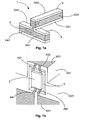
- inventive RFID transponder 1 is shown in a spatial representation.
- the embodiment shows the RFID transponder 1, which is formed from two carrier elements 3, 4, which are arranged in a T-shape.
- the support elements 3, 4 are arranged in different planes to each other and integrally connected to each other.
- the carrier element 4 is arranged below the carrier element 3.
- the arrangement of the carrier elements 3, 4 in different levels, the RFID transponder is suitable for attachment to two intersecting metallic rods.
- the support elements 3, 4 are each elongate, here cuboid-shaped elements, which consist of a dielectric, suitable for MID coating material. On two, respectively in relation to the other surfaces, long surfaces 031, 032, 041, 042 the support elements 3, 4 each have a metallization M31, M32, M41, M42 applied.
- the metallizations M31, M32 and the metallizations M41, M42 are each conductively connected to one another via two narrow sides of the carrier elements 3, 4 and thus each form an antenna 6, 7 on each of the carrier elements 3, 4.
- the two antennas 6, 7 each have two electrical connections A31, A32, A41, A42, by means of which the antennas 6, 7 are electrically connected to a chip 2.
- the chip comprises at least one transmitting and receiving circuit, and a memory.
- FIG. 1a A detailed view of the chip 2 from Fig. 1a is in the Fig. 1b shown.
- the chip 2 which is arranged in a depression 5 in the boundary region between the carrier elements 3, 4.
- the recess 5 is used merely to protect the chip 2, that this is protected from mechanical effects - wherein the recess 5 can be shed again with a plastic compound o. ⁇ .
- the antennas 6, 7 are electrically connected to the chip 2.
- the electrical connections A31, A32, A41, A42 are also produced by MID technology, metallic coatings on the surface of the support elements 3, 4, but can also be realized by soldered wires or otherwise.
- the chip can also be arranged at a different location on one of the carrier elements 3, 4, where an electrical contacting of the two antennas 6, 7 is offered.
- the Fig. 2 shows a further, inventive embodiment of an RFID transponder 1.
- the support elements 3, 4 are mounted in an L-shape to each other.
- the carrier element 4 is here mounted under the carrier element 3, so that the two carrier elements 3, 4 are located in different planes.
- inventive embodiments of the RFID transponder 1 such. a crossed shape, depending on the location of the RFID transponder 1 are conceivable.
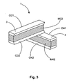
- FIG. 3 Another, inventive embodiment of an RFID transponder in T-shape - as in Fig. 1 shown - is in Fig. 3 shown.
- This embodiment additionally has a concave shape of the surfaces 032 and 042. This concave shape enables a better magnetic coupling of the antenna with round metal carriers 8, 9, on which the RFID transponder 2 is to be used.
- Such use of the RFID transponder 1 on round metal supports 8, 9 is in the Fig. 4 shown.
- the two, intersecting, round metal supports 8, 9 are indicated.
- the inventive RFID transponder 1 is provided with a housing 10 which electrically isolates the RFID transponder against the metal carrier 8, 9.
- the RFID transponder is attached to the metal carriers 8, 9 in such a way that the concave surface 032 of the carrier element 3 rests against the round metal carrier 9, and that the concave surface 042 of the carrier element 4 bears against the round metal carrier 8.
Landscapes
- Engineering & Computer Science (AREA)
- Physics & Mathematics (AREA)
- Computer Hardware Design (AREA)
- Microelectronics & Electronic Packaging (AREA)
- General Physics & Mathematics (AREA)
- Theoretical Computer Science (AREA)
- Computer Networks & Wireless Communication (AREA)
- Electromagnetism (AREA)
- Near-Field Transmission Systems (AREA)
Description
- Die Erfindung betrifft einen RFID-Transponder nach dem Oberbegriff des Anspruches 1.
- Gegenwärtig werden in vielen Bereichen, vor allem auch im Logistikbereich, sehr intensiv und nutzbringend RFID-Systeme eingesetzt. In vielen Fällen sind dabei sehr kompakte, flache RFID-Transponder notwendig.
- RFID-Transponder für solche Anwendungen sind beispielsweise aus der
EP 2 256 673 A1 bekannt. Hier wird ein Trägerelement zweiseitig, zumindest teilweise mit einer Metallisierung versehen. Die elektrisch verbundenen, eine Antenne bildenden Metallisierungen sind an einem auf dem Trägerelement vorgesehenen Chip angeschlossen. - Nachteilig wirkt sich bei dieser und ähnlichen Lösungen aus, dass die RFID-Transponder immer in mindestens eine Raumrichtung nicht abstrahlen. Dieser sog. Blind-Spot ist identisch mit der Dipolachse der Antenne und wirkt sich vor allem dann aus, wenn ein Transponder auf sich beweglichen Gegenständen angebracht ist und eine Ausleseeinheit sich möglicher Weise im Blind-Spot des RIFD-Transponders befindet.
- Aus dem Stand der Technik weiterhin bekannte Lösungen wie zum Beispiel Smart-Labels mit zwei Dipolachsen wirken diesem Problem zwar entgegen, sind jedoch sind für einen Einsatz auf Metalloberflächen nicht geeignet.
- Der Erfindung liegt daher die Aufgabe zugrunde, einen RFID-Transponder so auszubilden, dass er für den Einsatz auf einer Metalloberfläche geeignet ist und das Problem des auftretenden Blind-Spots nicht aufweist.
- Diese Aufgabe wird durch die Erfindung entsprechend dem kennzeichnenden Anspruch 1 gelöst.
- Vorteilhafte Ausgestaltungen der Erfindung sind in den Unteransprüchen angegeben.
- Bei der Erfindung handelt es sich um einen RFID-Transponder, der aus einem dielektrischen Trägerelement, auf welchem ein Chip und zwei Antennen angeordnet sind, gebildet wird. Der Chip umfasst dabei zumindest einen Sende- und einen Empfangsschaltkreis, sowie einen Speicher. Auf die genauere elektrische Funktionsweise des Chips wird in der Anmeldung nicht eingegangen, da diese nicht relevant ist.
- Die Antennen werden aus einer Metallschicht gebildet, welche auf der Oberfläche des Trägerelements aufgebracht ist. Dabei handelt es sich bei dem Trägerelement um ein Bauteil, welches vorzugsweise im MID-Verfahren mit einer metallischen, elektrisch leitenden Oberfläche beschichtet wurde. Diese im MID-Verfahren aufgebrachte Oberfläche wirkt als Antenne auf dem Trägerelement.
- Durch eine spezielle Ausbildung des Trägerelements, als quaderförmiges Bauteil, und einer metallischen Beschichtung an vier umlaufenden Seiten des Trägerelements bildet sich erfindungsgemäß eine Antenne mit einem Dipol aus.
- Erfindungsgemäß besteht der RFID-Transponder aus zwei solcher, jeweils als Antenne ausgebildeter Trägerelemente, welche vorzugsweise in einem rechten Winkel zueinander angeordnet sind. Die beiden Trägerelemente sind erfindungsgemäß einstückig und zweckmäßig als ein Spritzgussbauteil hergestellt. Bei Verwendung eines entsprechenden Substratmaterials ist eine Beschichtung des so entstandenen Grundkörpers im MID-Verfahren möglich um die Antennen auf der Oberfläche auszubilden.
- Die mit der Erfindung erzielten Vorteile bestehen insbesondere darin, dass die orthogonale Anordnung der zwei Antennen das Auftreten eines Blind-Spots verhindert. Speziell ist die Ausbildungsform der Trägerelemente für eine Nutzung des RFID-Transponders auf zwei metallischen Oberflächen vorgesehen. Dabei koppeln die Antennen des RFID-Transponders magnetisch mit der metallischen Oberfläche, auf der der RFID-Transponder genutzt wird, um die Strahlungscharakteristik des RFID-Transponders zu vergrößern.
- Ganz speziell ist der RFID-Transponders zur Nutzung an zwei, sich orthogonal kreuzenden Metallträgern vorgesehen. So bietet der erfindungsgemäße RFID-Transponder die Möglichkeit, an zwei sich kreuzenden, metallischen Stäben oder Trägern angebracht und genutzt zu werden.
- Dabei ist eine isolierende Schicht zwischen der metallisierten Oberfläche des RFID-Transponders und der metallischen Oberfläche, auf welcher der RFID-Transponder genutzt wird vorgesehen. Die isolierende Schicht kann ebenso als isolierendes Gehäuse um den RIFD-Transponder ausgebildet sein.
- Weitere Ausgestaltungen der Erfindung sind in den Unteransprüchen beschrieben.
- Ausführungsbeispiele der Erfindung sind in den Zeichnungen dargestellt und werden im Folgenden näher erläutert. Es zeigen:
- Fig. 1a
- einen RFID-Transponder in T-Bauform;
- Fig. 1b
- eine Detailansicht des RFID-Transponders aus
Fig. 1a ; - Fig. 2
- einen RFID-Transponder in L-Bauform;
- Fig. 3
- einen weiteren RFID-Transponder in T-Bauform; und
- Fig. 4
- einen RFID-Transponder aus
Fig. 3 im Einsatz. - In der
Fig.1 a ist ein in räumlicher Darstellung abgebildeter, erfindungsgemäßer RFID-Transponder 1 dargestellt. Die Ausführungsform zeigt den RFID-Transponder 1, der aus zwei Trägerelementen 3, 4 gebildet ist, welche in einer T-Bauform angeordnet sind. - Dabei sind die Trägerelemente 3, 4 in verschiedenen Ebenen zueinander angeordnet und einstückig miteinander verbunden. So ist in dieser gezeigten Ausführungsform das Trägerelement 4 unterhalb des Trägerelementes 3 angeordnet. Durch die Anordnung der Trägerelemente 3, 4 in verschiedenen Ebenen eignet sich der RFID-Transponder zur Anbringung an zwei sich kreuzende, metallische Stäbe.
- Die Trägerelemente 3, 4 sind jeweils längliche, hier quaderförmig ausgebildete Elemente, die aus einem dielektrischen, zur MID-Beschichtung geeigneten Material bestehen. Auf zwei, jeweils im Verhältnis zu den anderen Oberflächen, langen Oberflächen 031, 032, 041, 042 ist den Trägerelementen 3, 4 jeweils eine Metallisierung M31, M32, M41, M42 aufgebracht. Die Metallisierungen M31, M32, sowie die Metallisierungen M41, M42 sind jeweils über zwei schmale Seiten der Trägerelemente 3, 4 miteinander leitend verbunden und bilden so jeweils eine Antenne 6, 7 auf jedem der Trägerelemente 3, 4.
- Die zwei Antennen 6, 7 verfügen jeweils über zwei elektrische Anschlüsse A31, A32, A41, A42, mittels welcher die Antennen 6, 7 an einen Chip 2 elektrisch angeschlossen sind. Der Chip umfasst dabei zumindest einen Sende- und Empfangsschaltkreis, sowie einen Speicher. Durch den Anschluss der zwei vorzugsweise orthogonal, aber zumindest gewinkelt zueinander ausgerichteten Antennen 6, 7 optimiert sich erfindungsgemäß die Strahlungscharakteristik des RFID-Transponders 1.
- Eine Detailansicht des Chips 2 aus
Fig. 1a ist in derFig. 1b dargestellt. Zu erkennen ist der Chip 2 welcher in einer Vertiefung 5 im Grenzbereich zwischen den Trägerelementen 3, 4 angeordnet ist. Die Vertiefung 5 dient lediglich zum Schutz des Chips 2, dass dieser vor mechanischen Einwirkungen geschützt ist - wobei die Vertiefung 5 auch wieder mit einer Kunststoffmasse o. ä. vergossen werden kann. Mittels der elektrischen Anschlüsse A31, A32, A41, A42 sind die Antennen 6, 7 elektrisch mit dem Chip 2 verbunden. - Die elektrischen Anschlüsse A31, A32, A41, A42 sind ebenfalls durch MID-Technologie erzeugte, metallische Beschichtungen auf der Oberfläche der Trägerelemente 3, 4, können jedoch auch durch angelötete Drähte oder anders realisiert werden. Ebenso kann der Chip auch an einer anderen Stelle auf einem der Trägerelemente 3, 4 angeordnet werden, wo sich eine elektrische Kontaktierung der beiden Antennen 6, 7 anbietet.
- Die
Fig. 2 zeigt eine weitere, erfindungsgemäße Ausführungsform eines RFID-Transponders 1. In dieser sind die Trägerelemente 3, 4 in einer L-Bauform zueinander angebracht. Wie auch inFig. 1 a gezeigt, ist das Trägerelement 4 hier unter dem Trägerelement 3 angebracht, so dass sich die beiden Trägerelemente 3, 4 in verschiedenen Ebenen befinden. - Weitere, erfindungsgemäße Bauformen des RFID-Transponders 1, wie z.B. eine gekreuzte Form, sind je nach Einsatzort des RFID-Transponders 1 denkbar.
- Eine weitere, erfindungsgemäße Ausführungsform eines RFID-Transponders in T-Bauform - wie schon in
Fig. 1 dargestellt - ist inFig. 3 gezeigt. Diese Ausführungsform weist zusätzlich eine konkave Form der Oberflächen 032 und 042 auf. Durch diese konkave Form ist eine bessere magnetische Kopplung der Antenne mit runden Metallträgern 8, 9 möglich, auf welchem der RFID-Transponder 2 zum Einsatz kommen soll. - Ein solcher Einsatz des RFID-Transponders 1 auf runden Metallträgern 8, 9 ist in der
Fig. 4 dargestellt. Angedeutet sind die zwei, sich kreuzende, runde Metallträger 8 ,9 dargestellt. Der erfindungsgemäße RFID-Transponder 1 ist mit einem Gehäuse 10 versehen, welches den RFID-Transponder elektrisch gegen die Metallträger 8, 9 isoliert. Der RFID-Transponder ist so an den Metallträgern 8, 9 angebracht, dass die konkave Oberfläche 032 des Trägerelementes 3 an dem runden Metallträger 9 anliegt, und dass die konkave Oberfläche 042 des Trägerelements 4 an dem runden Metallträger 8 anliegt. -
- 1
- RFID-Transponder
- 2
- Chip
- 3
- Trägerelement
- 4
- Trägerelement
- 5
- Vertiefung
- 6
- Antenne von 3
- 7
- Antenne von 4
- 8
- Metallträger
- 9
- Metallträger
- 10
- isolierendes Gehäuse
- 031
- erste Oberfläche von 3
- 032
- zweite Oberfläche von 3
- 041
- erste Oberfläche von 4
- 042
- zweite Oberfläche von 4
- M31
- erste Metallisierung von 3
- M32
- zweite Metallisierung von 3
- M41
- erste Metallisierung von 4
- M42
- zweite Metallisierung von 4
- A31
- erster elektrischer Anschluss von 3
- A32
- zweiter elektrischer Anschluss von 3
- A41
- erster elektrischer Anschluss von 4
- A42
- zweiter elektrischer Anschluss von 4
Claims (5)
- RFID-Transponder (1), bestehend aus einem Chip (2), einer ersten Antenne (6) und einem, vorzugsweise länglich ausgebildeten, dielektrischen ersten Trägerelement (3),
wobei das erste Trägerelement (3) auf einer ersten Oberfläche (031) zumindest abschnittsweise mit einer ersten Metallisierung (M31) bedeckt ist, und
wobei das erste Trägerelemente (3) auf einer der ersten Oberfläche (O31) gegenüberliegenden, zweiten Oberfläche (032), zumindest abschnittsweise mit einer zweiten Metallisierung (M32) bedeckt ist, wobei die erste Metallisierung (M31) und die zweite Metallisierung (M32) miteinander elektrisch leitend, die erste Antenne (6) ausbildend, verbunden sind,
wobei die erste Antenne (6) zwei elektrische Anschlüsse (A31, A32) aufweist,
und wobei der Chip (2) über die Anschlüsse (A31, A32) elektrisch mit der ersten Antenne (6) verbunden ist,
wobei der RFID-Transponder (1) ein zweites Trägerelement (4) aufweist,
wobei die Trägerelemente (3, 4) einteilig ausgeführt sind,
und wobei der Chip (2) über elektrische Anschlüsse (A41, A42) des zweiten Trägerelementes (4) elektrisch mit einer zweite Antenne (7) verbunden ist.
wobei das zweite Trägerelement (4) auf einer ersten Oberfläche (041) zumindest abschnittsweise mit einer ersten Metallisierung (M41) bedeckt ist,
wobei das zweite Trägerelemente (4) auf einer der ersten Oberfläche (O41) gegenüberliegenden, zweiten Oberfläche (042), zumindest abschnittsweise mit einer zweiten Metallisierung (M42) bedeckt ist, wobei die erste Metallisierung (M41) und die zweite Metallisierung (M42) miteinander elektrisch leitend, die zweite Antenne (7) ausbildend, verbunden sind, dadurch gekennzeichnet,
dass die vorzugsweise länglich ausgebildeten Trägerelemente (3, 4) in verschiedenen Ebenen angeordnet sind. - RFID-Transponder (1) nach einem der vorstehenden Ansprüche,
dadurch gekennzeichnet,
dass die vorzugsweise länglich ausgebildeten Trägerelemente (3, 4) zueinander in etwa orthogonal ausgerichtet sind. - RFID-Transponder (1) nach einem der vorstehenden Ansprüche,
dadurch gekennzeichnet,
dass zumindest eine der metallisierten Oberflächen (031, 032, 041, 042) eine konkave Form aufweist. - RFID-Transponder (1) nach einem der vorstehenden Ansprüche,
dadurch gekennzeichnet,
dass der RFID-Transponder (2) von einem elektrisch isolierenden Gehäuse (10) umgeben ist. - RFID-Transponder (1) nach Anspruch 4, dadurch gekennzeichnet, dass das Gehäuse (10) in einem Spritzgussverfahren hergestellt, direkt um dem RFID-Transponder (1) geformt ist.
Priority Applications (1)
| Application Number | Priority Date | Filing Date | Title |
|---|---|---|---|
| PL13718101T PL2828802T3 (pl) | 2012-03-23 | 2013-03-22 | Transponder RFID |
Applications Claiming Priority (2)
| Application Number | Priority Date | Filing Date | Title |
|---|---|---|---|
| DE102012102505A DE102012102505A1 (de) | 2012-03-23 | 2012-03-23 | RFID-Transponder |
| PCT/DE2013/100112 WO2013139336A1 (de) | 2012-03-23 | 2013-03-22 | Rfid-transponder |
Publications (2)
| Publication Number | Publication Date |
|---|---|
| EP2828802A1 EP2828802A1 (de) | 2015-01-28 |
| EP2828802B1 true EP2828802B1 (de) | 2016-01-13 |
Family
ID=48170393
Family Applications (1)
| Application Number | Title | Priority Date | Filing Date |
|---|---|---|---|
| EP13718101.2A Not-in-force EP2828802B1 (de) | 2012-03-23 | 2013-03-22 | Rfid-transponder |
Country Status (5)
| Country | Link |
|---|---|
| EP (1) | EP2828802B1 (de) |
| DE (1) | DE102012102505A1 (de) |
| ES (1) | ES2568036T3 (de) |
| PL (1) | PL2828802T3 (de) |
| WO (1) | WO2013139336A1 (de) |
Family Cites Families (4)
| Publication number | Priority date | Publication date | Assignee | Title |
|---|---|---|---|---|
| JP2004511033A (ja) * | 2000-08-11 | 2004-04-08 | エスコート・メモリー・システムズ | Rfidタグ組立体およびシステム |
| EP1629443A4 (de) * | 2003-05-23 | 2009-04-01 | Symbol Technologies Inc | Rfid-relaiseinrichtung und verfahren zum weiterleiten eines rfid-signals |
| US20080024309A1 (en) * | 2006-07-25 | 2008-01-31 | International Business Machines Corporation | Rfid tags suitable for affixing to rectangular corners |
| PL2256673T3 (pl) | 2009-05-29 | 2014-04-30 | Fraunhofer Ges Forschung | Transponder RFID do montażu na metalu i sposób jego wytwarzania |
-
2012
- 2012-03-23 DE DE102012102505A patent/DE102012102505A1/de not_active Withdrawn
-
2013
- 2013-03-22 ES ES13718101.2T patent/ES2568036T3/es active Active
- 2013-03-22 PL PL13718101T patent/PL2828802T3/pl unknown
- 2013-03-22 WO PCT/DE2013/100112 patent/WO2013139336A1/de not_active Ceased
- 2013-03-22 EP EP13718101.2A patent/EP2828802B1/de not_active Not-in-force
Also Published As
| Publication number | Publication date |
|---|---|
| PL2828802T3 (pl) | 2016-06-30 |
| ES2568036T3 (es) | 2016-04-27 |
| EP2828802A1 (de) | 2015-01-28 |
| WO2013139336A1 (de) | 2013-09-26 |
| DE102012102505A1 (de) | 2013-09-26 |
Similar Documents
| Publication | Publication Date | Title |
|---|---|---|
| EP1588454B1 (de) | Antenne mit zumindest einem dipol oder einer dipolähnlichen strahleranordnung | |
| EP3367504B1 (de) | Antenne für eine rfid-lesevorrichtung und verfahren zum senden und/oder empfangen von rfid-signalen | |
| DE10350034A1 (de) | Antennenanordnung insbesondere für Radaranwendungen bei Kraftfahrzeugen | |
| DE102008059453A1 (de) | Transpondereinrichtung | |
| EP3776359B1 (de) | Fahrzeugidentifikationsmittel | |
| EP2649677A1 (de) | RFID-Transponder | |
| DE112009002384T5 (de) | Antenne und Drahtlose-IC-Bauelement | |
| EP1943614B1 (de) | Transponder | |
| DE102010040809A1 (de) | Planare Gruppenantenne mit in mehreren Ebenen angeordneten Antennenelementen | |
| EP2243192B1 (de) | Identifikationsmarke zur identifikation von objekten mit metallischer oberfläche | |
| EP2367233A1 (de) | Planares Antennensystem | |
| EP2223385B1 (de) | Planare breitbandige antenne | |
| DE102012101443B4 (de) | Planare Antennenanordnung | |
| EP2828802B1 (de) | Rfid-transponder | |
| DE202014001474U1 (de) | UHF- RFID- Transponder | |
| EP2618425B1 (de) | Antennenabdeckung | |
| WO2013189484A1 (de) | Rfid-transponder mit einer invertierten f-antenne | |
| DE102012107291B4 (de) | RFID-Tag mit polarisationsunabhängiger Antenne | |
| DE102012107561B4 (de) | RFID-Transponder mit einer planaren F-Antenne | |
| DE102016201978A1 (de) | Antennenvorrichtung und Antennengruppenvorrichtung für Millimeterwellen | |
| DE102013219377A1 (de) | Antennenanordnung mit antenneneinheit und verbindereinheit | |
| DE102020108588B4 (de) | Antennenvorrichtung | |
| DE202010012917U1 (de) | Modifizierte Monopolantenne | |
| DE10103965C2 (de) | Peilantenne | |
| DE102017012098B4 (de) | UHF-RFID-Transponder |
Legal Events
| Date | Code | Title | Description |
|---|---|---|---|
| PUAI | Public reference made under article 153(3) epc to a published international application that has entered the european phase |
Free format text: ORIGINAL CODE: 0009012 |
|
| 17P | Request for examination filed |
Effective date: 20140911 |
|
| AK | Designated contracting states |
Kind code of ref document: A1 Designated state(s): AL AT BE BG CH CY CZ DE DK EE ES FI FR GB GR HR HU IE IS IT LI LT LU LV MC MK MT NL NO PL PT RO RS SE SI SK SM TR |
|
| AX | Request for extension of the european patent |
Extension state: BA ME |
|
| DAX | Request for extension of the european patent (deleted) | ||
| GRAP | Despatch of communication of intention to grant a patent |
Free format text: ORIGINAL CODE: EPIDOSNIGR1 |
|
| INTG | Intention to grant announced |
Effective date: 20150713 |
|
| GRAS | Grant fee paid |
Free format text: ORIGINAL CODE: EPIDOSNIGR3 |
|
| GRAA | (expected) grant |
Free format text: ORIGINAL CODE: 0009210 |
|
| AK | Designated contracting states |
Kind code of ref document: B1 Designated state(s): AL AT BE BG CH CY CZ DE DK EE ES FI FR GB GR HR HU IE IS IT LI LT LU LV MC MK MT NL NO PL PT RO RS SE SI SK SM TR |
|
| REG | Reference to a national code |
Ref country code: GB Ref legal event code: FG4D Free format text: NOT ENGLISH |
|
| REG | Reference to a national code |
Ref country code: CH Ref legal event code: EP |
|
| REG | Reference to a national code |
Ref country code: IE Ref legal event code: FG4D Free format text: LANGUAGE OF EP DOCUMENT: GERMAN |
|
| REG | Reference to a national code |
Ref country code: AT Ref legal event code: REF Ref document number: 770964 Country of ref document: AT Kind code of ref document: T Effective date: 20160215 |
|
| REG | Reference to a national code |
Ref country code: DE Ref legal event code: R096 Ref document number: 502013001814 Country of ref document: DE |
|
| REG | Reference to a national code |
Ref country code: ES Ref legal event code: FG2A Ref document number: 2568036 Country of ref document: ES Kind code of ref document: T3 Effective date: 20160427 |
|
| PGFP | Annual fee paid to national office [announced via postgrant information from national office to epo] |
Ref country code: TR Payment date: 20160316 Year of fee payment: 4 Ref country code: ES Payment date: 20160311 Year of fee payment: 4 |
|
| REG | Reference to a national code |
Ref country code: LT Ref legal event code: MG4D |
|
| REG | Reference to a national code |
Ref country code: NL Ref legal event code: MP Effective date: 20160113 |
|
| PG25 | Lapsed in a contracting state [announced via postgrant information from national office to epo] |
Ref country code: NL Free format text: LAPSE BECAUSE OF FAILURE TO SUBMIT A TRANSLATION OF THE DESCRIPTION OR TO PAY THE FEE WITHIN THE PRESCRIBED TIME-LIMIT Effective date: 20160113 |
|
| PG25 | Lapsed in a contracting state [announced via postgrant information from national office to epo] |
Ref country code: FI Free format text: LAPSE BECAUSE OF FAILURE TO SUBMIT A TRANSLATION OF THE DESCRIPTION OR TO PAY THE FEE WITHIN THE PRESCRIBED TIME-LIMIT Effective date: 20160113 Ref country code: GR Free format text: LAPSE BECAUSE OF FAILURE TO SUBMIT A TRANSLATION OF THE DESCRIPTION OR TO PAY THE FEE WITHIN THE PRESCRIBED TIME-LIMIT Effective date: 20160414 Ref country code: HR Free format text: LAPSE BECAUSE OF FAILURE TO SUBMIT A TRANSLATION OF THE DESCRIPTION OR TO PAY THE FEE WITHIN THE PRESCRIBED TIME-LIMIT Effective date: 20160113 Ref country code: NO Free format text: LAPSE BECAUSE OF FAILURE TO SUBMIT A TRANSLATION OF THE DESCRIPTION OR TO PAY THE FEE WITHIN THE PRESCRIBED TIME-LIMIT Effective date: 20160413 |
|
| PG25 | Lapsed in a contracting state [announced via postgrant information from national office to epo] |
Ref country code: BE Free format text: LAPSE BECAUSE OF NON-PAYMENT OF DUE FEES Effective date: 20160331 Ref country code: IS Free format text: LAPSE BECAUSE OF FAILURE TO SUBMIT A TRANSLATION OF THE DESCRIPTION OR TO PAY THE FEE WITHIN THE PRESCRIBED TIME-LIMIT Effective date: 20160513 Ref country code: RS Free format text: LAPSE BECAUSE OF FAILURE TO SUBMIT A TRANSLATION OF THE DESCRIPTION OR TO PAY THE FEE WITHIN THE PRESCRIBED TIME-LIMIT Effective date: 20160113 Ref country code: SE Free format text: LAPSE BECAUSE OF FAILURE TO SUBMIT A TRANSLATION OF THE DESCRIPTION OR TO PAY THE FEE WITHIN THE PRESCRIBED TIME-LIMIT Effective date: 20160113 Ref country code: LT Free format text: LAPSE BECAUSE OF FAILURE TO SUBMIT A TRANSLATION OF THE DESCRIPTION OR TO PAY THE FEE WITHIN THE PRESCRIBED TIME-LIMIT Effective date: 20160113 Ref country code: LV Free format text: LAPSE BECAUSE OF FAILURE TO SUBMIT A TRANSLATION OF THE DESCRIPTION OR TO PAY THE FEE WITHIN THE PRESCRIBED TIME-LIMIT Effective date: 20160113 Ref country code: PT Free format text: LAPSE BECAUSE OF FAILURE TO SUBMIT A TRANSLATION OF THE DESCRIPTION OR TO PAY THE FEE WITHIN THE PRESCRIBED TIME-LIMIT Effective date: 20160513 |
|
| PGFP | Annual fee paid to national office [announced via postgrant information from national office to epo] |
Ref country code: PL Payment date: 20160318 Year of fee payment: 4 Ref country code: IT Payment date: 20160331 Year of fee payment: 4 |
|
| REG | Reference to a national code |
Ref country code: DE Ref legal event code: R081 Ref document number: 502013001814 Country of ref document: DE Owner name: HARTING IT SOFTWARE DEVELOPMENT GMBH & CO. KG, DE Free format text: FORMER OWNER: HARTING ELECTRIC GMBH & CO. KG, 32339 ESPELKAMP, DE |
|
| REG | Reference to a national code |
Ref country code: DE Ref legal event code: R097 Ref document number: 502013001814 Country of ref document: DE |
|
| PG25 | Lapsed in a contracting state [announced via postgrant information from national office to epo] |
Ref country code: MC Free format text: LAPSE BECAUSE OF FAILURE TO SUBMIT A TRANSLATION OF THE DESCRIPTION OR TO PAY THE FEE WITHIN THE PRESCRIBED TIME-LIMIT Effective date: 20160113 Ref country code: EE Free format text: LAPSE BECAUSE OF FAILURE TO SUBMIT A TRANSLATION OF THE DESCRIPTION OR TO PAY THE FEE WITHIN THE PRESCRIBED TIME-LIMIT Effective date: 20160113 Ref country code: LU Free format text: LAPSE BECAUSE OF FAILURE TO SUBMIT A TRANSLATION OF THE DESCRIPTION OR TO PAY THE FEE WITHIN THE PRESCRIBED TIME-LIMIT Effective date: 20160322 Ref country code: DK Free format text: LAPSE BECAUSE OF FAILURE TO SUBMIT A TRANSLATION OF THE DESCRIPTION OR TO PAY THE FEE WITHIN THE PRESCRIBED TIME-LIMIT Effective date: 20160113 |
|
| REG | Reference to a national code |
Ref country code: CH Ref legal event code: PL |
|
| PLBE | No opposition filed within time limit |
Free format text: ORIGINAL CODE: 0009261 |
|
| STAA | Information on the status of an ep patent application or granted ep patent |
Free format text: STATUS: NO OPPOSITION FILED WITHIN TIME LIMIT |
|
| PG25 | Lapsed in a contracting state [announced via postgrant information from national office to epo] |
Ref country code: SM Free format text: LAPSE BECAUSE OF FAILURE TO SUBMIT A TRANSLATION OF THE DESCRIPTION OR TO PAY THE FEE WITHIN THE PRESCRIBED TIME-LIMIT Effective date: 20160113 Ref country code: CZ Free format text: LAPSE BECAUSE OF FAILURE TO SUBMIT A TRANSLATION OF THE DESCRIPTION OR TO PAY THE FEE WITHIN THE PRESCRIBED TIME-LIMIT Effective date: 20160113 Ref country code: RO Free format text: LAPSE BECAUSE OF FAILURE TO SUBMIT A TRANSLATION OF THE DESCRIPTION OR TO PAY THE FEE WITHIN THE PRESCRIBED TIME-LIMIT Effective date: 20160113 Ref country code: SK Free format text: LAPSE BECAUSE OF FAILURE TO SUBMIT A TRANSLATION OF THE DESCRIPTION OR TO PAY THE FEE WITHIN THE PRESCRIBED TIME-LIMIT Effective date: 20160113 |
|
| 26N | No opposition filed |
Effective date: 20161014 |
|
| REG | Reference to a national code |
Ref country code: IE Ref legal event code: MM4A |
|
| REG | Reference to a national code |
Ref country code: FR Ref legal event code: ST Effective date: 20161130 |
|
| PG25 | Lapsed in a contracting state [announced via postgrant information from national office to epo] |
Ref country code: CH Free format text: LAPSE BECAUSE OF NON-PAYMENT OF DUE FEES Effective date: 20160331 Ref country code: FR Free format text: LAPSE BECAUSE OF NON-PAYMENT OF DUE FEES Effective date: 20160331 Ref country code: IE Free format text: LAPSE BECAUSE OF NON-PAYMENT OF DUE FEES Effective date: 20160322 Ref country code: LI Free format text: LAPSE BECAUSE OF NON-PAYMENT OF DUE FEES Effective date: 20160331 |
|
| PG25 | Lapsed in a contracting state [announced via postgrant information from national office to epo] |
Ref country code: BG Free format text: LAPSE BECAUSE OF FAILURE TO SUBMIT A TRANSLATION OF THE DESCRIPTION OR TO PAY THE FEE WITHIN THE PRESCRIBED TIME-LIMIT Effective date: 20160413 Ref country code: SI Free format text: LAPSE BECAUSE OF FAILURE TO SUBMIT A TRANSLATION OF THE DESCRIPTION OR TO PAY THE FEE WITHIN THE PRESCRIBED TIME-LIMIT Effective date: 20160113 |
|
| PG25 | Lapsed in a contracting state [announced via postgrant information from national office to epo] |
Ref country code: MT Free format text: LAPSE BECAUSE OF FAILURE TO SUBMIT A TRANSLATION OF THE DESCRIPTION OR TO PAY THE FEE WITHIN THE PRESCRIBED TIME-LIMIT Effective date: 20160113 |
|
| PG25 | Lapsed in a contracting state [announced via postgrant information from national office to epo] |
Ref country code: IT Free format text: LAPSE BECAUSE OF NON-PAYMENT OF DUE FEES Effective date: 20170322 |
|
| PG25 | Lapsed in a contracting state [announced via postgrant information from national office to epo] |
Ref country code: HU Free format text: LAPSE BECAUSE OF FAILURE TO SUBMIT A TRANSLATION OF THE DESCRIPTION OR TO PAY THE FEE WITHIN THE PRESCRIBED TIME-LIMIT; INVALID AB INITIO Effective date: 20130322 |
|
| REG | Reference to a national code |
Ref country code: ES Ref legal event code: FD2A Effective date: 20180625 |
|
| PG25 | Lapsed in a contracting state [announced via postgrant information from national office to epo] |
Ref country code: CY Free format text: LAPSE BECAUSE OF FAILURE TO SUBMIT A TRANSLATION OF THE DESCRIPTION OR TO PAY THE FEE WITHIN THE PRESCRIBED TIME-LIMIT Effective date: 20160113 Ref country code: MK Free format text: LAPSE BECAUSE OF FAILURE TO SUBMIT A TRANSLATION OF THE DESCRIPTION OR TO PAY THE FEE WITHIN THE PRESCRIBED TIME-LIMIT Effective date: 20160113 |
|
| PG25 | Lapsed in a contracting state [announced via postgrant information from national office to epo] |
Ref country code: ES Free format text: LAPSE BECAUSE OF NON-PAYMENT OF DUE FEES Effective date: 20170323 |
|
| PG25 | Lapsed in a contracting state [announced via postgrant information from national office to epo] |
Ref country code: PL Free format text: LAPSE BECAUSE OF NON-PAYMENT OF DUE FEES Effective date: 20170322 Ref country code: AL Free format text: LAPSE BECAUSE OF FAILURE TO SUBMIT A TRANSLATION OF THE DESCRIPTION OR TO PAY THE FEE WITHIN THE PRESCRIBED TIME-LIMIT Effective date: 20160113 |
|
| REG | Reference to a national code |
Ref country code: AT Ref legal event code: MM01 Ref document number: 770964 Country of ref document: AT Kind code of ref document: T Effective date: 20180322 |
|
| PG25 | Lapsed in a contracting state [announced via postgrant information from national office to epo] |
Ref country code: AT Free format text: LAPSE BECAUSE OF NON-PAYMENT OF DUE FEES Effective date: 20180322 |
|
| PG25 | Lapsed in a contracting state [announced via postgrant information from national office to epo] |
Ref country code: TR Free format text: LAPSE BECAUSE OF NON-PAYMENT OF DUE FEES Effective date: 20170322 |
|
| P01 | Opt-out of the competence of the unified patent court (upc) registered |
Effective date: 20230603 |
|
| PGFP | Annual fee paid to national office [announced via postgrant information from national office to epo] |
Ref country code: DE Payment date: 20240328 Year of fee payment: 12 Ref country code: GB Payment date: 20240319 Year of fee payment: 12 |
|
| REG | Reference to a national code |
Ref country code: DE Ref legal event code: R119 Ref document number: 502013001814 Country of ref document: DE |
|
| GBPC | Gb: european patent ceased through non-payment of renewal fee |
Effective date: 20250322 |
|
| PG25 | Lapsed in a contracting state [announced via postgrant information from national office to epo] |
Ref country code: DE Free format text: LAPSE BECAUSE OF NON-PAYMENT OF DUE FEES Effective date: 20251001 |
|
| PG25 | Lapsed in a contracting state [announced via postgrant information from national office to epo] |
Ref country code: GB Free format text: LAPSE BECAUSE OF NON-PAYMENT OF DUE FEES Effective date: 20250322 |