EP2829508A2 - Einkapselungsstruktur, die eine mechanisch verstärkte Hülle mit Getter-Effekt umfasst - Google Patents
Einkapselungsstruktur, die eine mechanisch verstärkte Hülle mit Getter-Effekt umfasst Download PDFInfo
- Publication number
- EP2829508A2 EP2829508A2 EP14178068.4A EP14178068A EP2829508A2 EP 2829508 A2 EP2829508 A2 EP 2829508A2 EP 14178068 A EP14178068 A EP 14178068A EP 2829508 A2 EP2829508 A2 EP 2829508A2
- Authority
- EP
- European Patent Office
- Prior art keywords
- layer
- reinforcing portions
- mechanical reinforcing
- encapsulation
- micro
- Prior art date
- Legal status (The legal status is an assumption and is not a legal conclusion. Google has not performed a legal analysis and makes no representation as to the accuracy of the status listed.)
- Granted
Links
Images


Classifications
-
- B—PERFORMING OPERATIONS; TRANSPORTING
- B81—MICROSTRUCTURAL TECHNOLOGY
- B81B—MICROSTRUCTURAL DEVICES OR SYSTEMS, e.g. MICROMECHANICAL DEVICES
- B81B7/00—Microstructural systems ; Auxiliary parts of microstructural devices or systems
- B81B7/0032—Packages or encapsulation
- B81B7/0058—Packages or encapsulation for protecting against damages due to external chemical or mechanical influences, e.g. shocks or vibrations
-
- B—PERFORMING OPERATIONS; TRANSPORTING
- B81—MICROSTRUCTURAL TECHNOLOGY
- B81B—MICROSTRUCTURAL DEVICES OR SYSTEMS, e.g. MICROMECHANICAL DEVICES
- B81B7/00—Microstructural systems ; Auxiliary parts of microstructural devices or systems
- B81B7/0032—Packages or encapsulation
- B81B7/0035—Packages or encapsulation for maintaining a controlled atmosphere inside of the chamber containing the MEMS
- B81B7/0038—Packages or encapsulation for maintaining a controlled atmosphere inside of the chamber containing the MEMS using materials for controlling the level of pressure, contaminants or moisture inside of the package, e.g. getters
-
- B—PERFORMING OPERATIONS; TRANSPORTING
- B81—MICROSTRUCTURAL TECHNOLOGY
- B81B—MICROSTRUCTURAL DEVICES OR SYSTEMS, e.g. MICROMECHANICAL DEVICES
- B81B7/00—Microstructural systems ; Auxiliary parts of microstructural devices or systems
- B81B7/0032—Packages or encapsulation
- B81B7/0077—Other packages not provided for in groups B81B7/0035 - B81B7/0074
-
- B—PERFORMING OPERATIONS; TRANSPORTING
- B81—MICROSTRUCTURAL TECHNOLOGY
- B81C—PROCESSES OR APPARATUS SPECIALLY ADAPTED FOR THE MANUFACTURE OR TREATMENT OF MICROSTRUCTURAL DEVICES OR SYSTEMS
- B81C1/00—Manufacture or treatment of devices or systems in or on a substrate
- B81C1/00015—Manufacture or treatment of devices or systems in or on a substrate for manufacturing microsystems
- B81C1/00261—Processes for packaging MEMS devices
- B81C1/00277—Processes for packaging MEMS devices for maintaining a controlled atmosphere inside of the cavity containing the MEMS
- B81C1/00285—Processes for packaging MEMS devices for maintaining a controlled atmosphere inside of the cavity containing the MEMS using materials for controlling the level of pressure, contaminants or moisture inside of the package, e.g. getters
-
- B—PERFORMING OPERATIONS; TRANSPORTING
- B81—MICROSTRUCTURAL TECHNOLOGY
- B81C—PROCESSES OR APPARATUS SPECIALLY ADAPTED FOR THE MANUFACTURE OR TREATMENT OF MICROSTRUCTURAL DEVICES OR SYSTEMS
- B81C1/00—Manufacture or treatment of devices or systems in or on a substrate
- B81C1/00015—Manufacture or treatment of devices or systems in or on a substrate for manufacturing microsystems
- B81C1/00261—Processes for packaging MEMS devices
- B81C1/00301—Connecting electric signal lines from the MEMS device with external electrical signal lines, e.g. through vias
-
- B—PERFORMING OPERATIONS; TRANSPORTING
- B81—MICROSTRUCTURAL TECHNOLOGY
- B81C—PROCESSES OR APPARATUS SPECIALLY ADAPTED FOR THE MANUFACTURE OR TREATMENT OF MICROSTRUCTURAL DEVICES OR SYSTEMS
- B81C1/00—Manufacture or treatment of devices or systems in or on a substrate
- B81C1/00642—Manufacture or treatment of devices or systems in or on a substrate for improving the physical properties of a device
- B81C1/0065—Mechanical properties
- B81C1/00682—Treatments for improving mechanical properties, not provided for in B81C1/00658 - B81C1/0065
-
- B—PERFORMING OPERATIONS; TRANSPORTING
- B81—MICROSTRUCTURAL TECHNOLOGY
- B81B—MICROSTRUCTURAL DEVICES OR SYSTEMS, e.g. MICROMECHANICAL DEVICES
- B81B2201/00—Specific applications of microelectromechanical systems
- B81B2201/02—Sensors
- B81B2201/0228—Inertial sensors
-
- B—PERFORMING OPERATIONS; TRANSPORTING
- B81—MICROSTRUCTURAL TECHNOLOGY
- B81B—MICROSTRUCTURAL DEVICES OR SYSTEMS, e.g. MICROMECHANICAL DEVICES
- B81B2207/00—Microstructural systems or auxiliary parts thereof
- B81B2207/09—Packages
- B81B2207/091—Arrangements for connecting external electrical signals to mechanical structures inside the package
- B81B2207/094—Feed-through, via
- B81B2207/096—Feed-through, via through the substrate
-
- B—PERFORMING OPERATIONS; TRANSPORTING
- B81—MICROSTRUCTURAL TECHNOLOGY
- B81C—PROCESSES OR APPARATUS SPECIALLY ADAPTED FOR THE MANUFACTURE OR TREATMENT OF MICROSTRUCTURAL DEVICES OR SYSTEMS
- B81C2201/00—Manufacture or treatment of microstructural devices or systems
- B81C2201/05—Temporary protection of devices or parts of the devices during manufacturing
- B81C2201/053—Depositing a protective layers
-
- B—PERFORMING OPERATIONS; TRANSPORTING
- B81—MICROSTRUCTURAL TECHNOLOGY
- B81C—PROCESSES OR APPARATUS SPECIALLY ADAPTED FOR THE MANUFACTURE OR TREATMENT OF MICROSTRUCTURAL DEVICES OR SYSTEMS
- B81C2203/00—Forming microstructural systems
- B81C2203/01—Packaging MEMS
- B81C2203/0136—Growing or depositing of a covering layer
-
- B—PERFORMING OPERATIONS; TRANSPORTING
- B81—MICROSTRUCTURAL TECHNOLOGY
- B81C—PROCESSES OR APPARATUS SPECIALLY ADAPTED FOR THE MANUFACTURE OR TREATMENT OF MICROSTRUCTURAL DEVICES OR SYSTEMS
- B81C2203/00—Forming microstructural systems
- B81C2203/01—Packaging MEMS
- B81C2203/0163—Reinforcing a cap, e.g. with ribs
-
- H—ELECTRICITY
- H10—SEMICONDUCTOR DEVICES; ELECTRIC SOLID-STATE DEVICES NOT OTHERWISE PROVIDED FOR
- H10W—GENERIC PACKAGES, INTERCONNECTIONS, CONNECTORS OR OTHER CONSTRUCTIONAL DETAILS OF DEVICES COVERED BY CLASS H10
- H10W90/00—Package configurations
- H10W90/701—Package configurations characterised by the relative positions of pads or connectors relative to package parts
- H10W90/721—Package configurations characterised by the relative positions of pads or connectors relative to package parts of bump connectors
- H10W90/722—Package configurations characterised by the relative positions of pads or connectors relative to package parts of bump connectors between stacked chips
-
- H—ELECTRICITY
- H10—SEMICONDUCTOR DEVICES; ELECTRIC SOLID-STATE DEVICES NOT OTHERWISE PROVIDED FOR
- H10W—GENERIC PACKAGES, INTERCONNECTIONS, CONNECTORS OR OTHER CONSTRUCTIONAL DETAILS OF DEVICES COVERED BY CLASS H10
- H10W90/00—Package configurations
- H10W90/701—Package configurations characterised by the relative positions of pads or connectors relative to package parts
- H10W90/721—Package configurations characterised by the relative positions of pads or connectors relative to package parts of bump connectors
- H10W90/724—Package configurations characterised by the relative positions of pads or connectors relative to package parts of bump connectors between a chip and a stacked insulating package substrate, interposer or RDL
Definitions
- the invention relates to the field of encapsulation structures comprising one or more micro-devices encapsulated in one or more cavities hermetically, for example under a controlled atmosphere.
- the invention is advantageously applied to the encapsulation of micro-devices of the MEMS (electromechanical microsystem) resonant type.
- micro-device denotes any microsystem of the MEMS, NEMS (electromechanical nanosystem), MOEMS (opto-electromechanical microsystem), NOEMS (optoelectromechanical nanosystem) type, as well as any type of electronic, optical, or optoelectronic component or microcomponent. .
- the document FR 2 901 264 describes the production of mechanical reinforcements in the form of projections at the level of the top wall of a cover obtained by deposition of one or more thin layers. This method is, however, compatible only with the production of thin-film hoods and not with the production of hoods by the transfer of substrates. In addition, with such reinforcements made outside the cavity, there is a strong risk that delamination occurs between the reinforcements and the cover because if the assembly defined by the projecting elements is more mechanically rigid than the hood, the forces exerted on the hood can then cause a delamination between the hood and the reinforcements. Finally, the reinforcements described in this document are not sufficient for the encapsulation structure to withstand pressures greater than or equal to about 100 bar, which correspond to the pressures encountered during the implementation of a step overmolding the microphone. device thus encapsulated.
- the document FR 2 955 999 describes the mechanical reinforcement of a cover obtained by deposition of one or more thin layers, via a localized deposit of a portion of mechanical reinforcing material covering the cover.
- the mechanical reinforcement obtained is satisfactory in terms of the mechanical strength provided to the cover, the reinforcing zone thus continues over the entire surface of the cover prevents access to the cover or the micro-device, preventing for example to carry out checks or optical measurements on the inside of the hood or on the encapsulated micro-device.
- the residual stresses that are localized at the interface between the reinforcing material and the encapsulation layer can have a detrimental effect on the mechanical strength of the the interface.
- this method is only compatible with the production of thin-film hoods and not with hoods formed by the transfer of substrates.
- An object of the present invention is to provide an encapsulation structure whose cover is mechanically reinforced, which is compatible with a thin film packaging or substrate transfer, and whose encapsulation atmosphere can be easily controlled.
- the mechanical reinforcement portions thus integrated into the cover stiffen and strongly consolidate the encapsulation structure and make it resistant in particular to the subsequent steps of manipulation and packaging that the encapsulation structure is intended to undergo. Moreover, by producing these mechanical reinforcing portions at the inner wall of the cavity and with a material whose Young's modulus is greater than that of the hood layer material, the production of such a cover is compatible. as much with a thin-layer packaging as with a packaging substrate transfer advantageously thinned. This structure encapsulation only uses elements that are compatible with conventional microelectronics techniques.
- the mechanical reinforcing portions have absorption and / or gas adsorption properties, that is to say integrate a getter function that will allow to control the atmosphere in the cavity, both in terms of of nature and partial pressure of the residual gases in the cavity.
- Such an encapsulation structure is advantageously used to protect micro-devices for example MEMS of the inertial type comprising moving parts (free or embedded beams, membranes, seismic masses, microtubes, etc.), before their integration into a line of final packaging. This is further achieved through low cost, collective manufacturing technologies.
- Such an encapsulation structure can also be carried directly on a printed circuit board (PCB) ("Printed Circuit Board").
- PCB printed circuit board
- the second material may be a metallic getter material.
- Each of the mechanical reinforcing portions may comprise at least a first layer of the second material and at least a second layer of a third metal getter material such that the first layer of the second material is disposed between the layer of the first material and the second layer of the second material. third material and / or is covered by the second layer of the third material.
- each of the mechanical reinforcing portions with these different layers of materials makes it possible to overcome the constraints related to the maximum thicknesses for producing the materials used to form the mechanical reinforcing portions.
- Such a multilayer structure of the mechanical reinforcing portions is advantageously used to produce mechanical reinforcing portions whose thickness is greater than about 0.5 ⁇ m.
- the first layer of the second material can serve as an activation temperature adjustment sub-layer.
- thermal third metal getter material may in this case be a metal such as Cr and / or Ti and / or Co and / or Fe and / or Mn and / or Mo and / or Ta and / or V and / or or W, and / or preferably Ru and / or Pt and / or Cr and / or Ni. Details of making such an adjustment sub-layer are described for example in the document FR 2 922 202 .
- Each of the mechanical reinforcing portions may comprise a stack of layers of which at least two of said layers form a bimetal exerting on the cover a force directed towards the outside of the cavity.
- the two layers forming the bimetallic strip may correspond to the first layer of the second material and to the second layer of the third metal getter material.
- the first material may be based on Si and / or silica and / or silicon nitride
- the second material may be based on Cr and / or Ti and / or Co and / or Fe and / or Mn and / or Mo and / or Ta and / or V and / or W and / or Pd and / or Rh and / or Pt and / or Ru and / or Zr.
- one of the metallic getter materials comprises Zr
- this material may be associated with one of the other materials mentioned above, the Young's modulus of which is greater than that of the first material.
- the metal getter material (s) may be based on Cr and / or Ti and / or Co and / or Fe and / or Mn and / or Mo and / or Ta and / or V and / or W and / or Pd and / or Rh and / or Pt and / or Ru and / or Zr.
- the term "based on” can refer to both the material in question and one of its alloys.
- Each of the mechanical reinforcing portions may be of substantially rectangular parallelepiped shape, the mechanical reinforcing portions being able to be arranged substantially parallel to one another.
- the mechanical reinforcing portions may form a mesh on said face of the layer of the first material.
- the encapsulation structure may further comprise electrically conductive vias made through the thickness of the substrate and / or the layer of the first material, next to the cavity. Such vias may form, for example, electrical access to the encapsulated micro-device.
- the invention also relates to a microelectronic device comprising at least two encapsulation structures as described above and arranged one above the other, in which at least one electrically conductive via a first of the two structures encapsulation is electrically connected to at least one electrically conductive via a second of the two encapsulation structures directly or via an interposer.
- a microelectronic device comprising at least two encapsulation structures as described above and arranged one above the other, in which at least one electrically conductive via a first of the two structures encapsulation is electrically connected to at least one electrically conductive via a second of the two encapsulation structures directly or via an interposer.
- Such a substrate transfer encapsulation method makes it possible to obtain an encapsulation structure as described above.
- Such a method also corresponds to a method of encapsulation by transfer of a cap formed by deposition of one or more thin layers in a mold.
- Each of the mechanical reinforcing portions may be made at least by depositing a first layer of the second material and a second layer of a third metal getter material such that the first layer of the second material is disposed between the first layer of the first material material and the second layer of the third material and / or is covered by the second layer of the third material.
- Each of the mechanical reinforcing portions may be made by depositing a stack of layers, at least two of said layers form a bimetal exerting on the cover a force directed towards the outside of the cavity.
- the method may further comprise, after the fastening of the cover to the substrate or the etching of the portion of sacrificial material, the production of electrically conductive vias through the thickness of the substrate and / or the layer of the first material, next to the cavity.
- the invention finally relates to a method for producing a microelectronic device, comprising the implementation of an encapsulation method as described above and forming at least two encapsulation structures, said encapsulation structures being arranged one above the other, at least one electrically conductive via a first of the two encapsulation structures then being electrically connected to at least one electrically conductive via a second of the two encapsulation structures directly or through an interposer.
- FIG. 1 represents a sectional view of an encapsulation structure 100 according to a first embodiment.
- the encapsulation structure 100 comprises a substrate 102 in which a micro-device 104 is produced.
- This micro-device 104 is, for example, an inertial-type MEMS comprising one or more moving parts (beams, membranes, seismic masses, microtubes, etc. .).
- a cover 106 is secured to the substrate 102 by means of a sealing bead 108 which laterally delimits a cavity 110 in which the micro-device 104 is encapsulated.
- the cover 106 comprises a layer 112 of a first material corresponding to a thinned substrate whose thickness is for example between about 5 microns and 100 microns.
- a face 114 of the layer 112 forms an inner wall of the cavity 110, here an upper wall of the cavity 110.
- mechanical reinforcing portions 116 having gas absorption and / or adsorption properties and comprising at least a metal getter material are made against the face 114 of the layer 112, fulfilling the dual function of gaseous pumping and mechanical reinforcement of the cover 106.
- a first embodiment of the cover 106 is described in connection with the figures 2 and 3 respectively showing a profile sectional view and a bottom view of a portion of the hood 106.
- each of the mechanical reinforcing portions 116 is of rectangular parallelepipedal shape and is arranged against the face 114 of the layer 112. These mechanical reinforcing portions 116 are arranged next to each other and parallel to each other (and are oriented parallel to the Y axis in the example shown in FIGS. figures 2 and 3 ). Each of the mechanical reinforcing portions 116 has a length I (dimension along the Y axis) substantially corresponding to the width of the portion of the face 114 which forms the upper wall of the cavity 110 (which depends in particular on the dimensions of the cavity 110). and therefore dimensions of the encapsulated micro-device 104).
- the mechanical reinforcing portions 116 are distributed over the entire length of this portion of the face 114 in order to mechanically consolidate the assembly of the upper wall of the cavity 110.
- the peripheral portions of the face 114 which are not covered by the portions mechanical reinforcement 116 correspond in particular to the parts of the layer 112 intended to be in contact with the sealing bead 108.
- Each of the mechanical reinforcing portions 116 has a width b (dimension along the X axis), these portions 116 being furthermore arranged side by side with a period t, this period being equal to the sum of the width b and the space separating two mechanical reinforcing portions.
- the layer 112 has a thickness h (dimension along the Z axis), and the cap 106 has an overall thickness H equal to the sum of the thickness h of the layer 112 and the thickness of the mechanical reinforcing portions. 116 (each mechanical reinforcing portion 116 therefore has a thickness equal to Hh).
- each of the mechanical reinforcing portions 116 fulfill both their role of mechanical reinforcement of the cover 106 and gaseous pumping, these portions 116 are made, in this first embodiment, with a metal getter material whose Young's modulus is greater than or equal to that of the first material of the layer 112 (this first material corresponding here to silicon, whose Young's modulus is equal to about 110 GPa).
- each of the mechanical reinforcing portions 116 comprises a portion of one or more of the following materials: chromium, molybdenum, tantalum, tungsten, vanadium, cobalt, iron, manganese, nickel, copper, ruthenium, platinum.
- the mechanical reinforcing portions 116 may further comprise hafnium and / or niobium and / or titanium.
- the ratios r and R can be chosen as indicated in the table below: M O r R 2 2 [0.6-0.8] ⁇ 0.8 2 5 [0.6-0.8] ⁇ 0.7 3 2 [0.6-0.8] ⁇ 0.7 3 5 [0.6-0.9] ⁇ 0.8
- the mechanical reinforcing portions 116 may be sized such that: O H ( ⁇ m) b ( ⁇ m) h ( ⁇ m) t ( ⁇ m) (Hh) ( ⁇ m) 2 50 25 [30 - 40] ⁇ 35.7 [10 - 20] 5 50 10 [30 - 45] ⁇ 12.5 [5 - 20]
- the mechanical reinforcing portions 116 may comprise several layers, or parts, of different materials superimposed one above the other. So, on the figure 4 each of the mechanical reinforcing portions 116 comprises a first layer of material 118 and a second layer of material 120 disposed one above the other such that the first layer 118 is disposed between the face 114 of the layer 112 and the second layer 120. According to another variant embodiment shown in FIG. figure 5 for each of the mechanical reinforcing portions 116, the second layer 120 completely covers the first layer 118. According to these variants, the second layer 120 may comprise one or more getter materials such as those previously described, or else titanium and / or zirconium or an alloy based on titanium or zirconium having a getter effect.
- each of these mechanical reinforcing portions 116 formed of several layers of different materials it is possible to use a metallic getter material to make the upper layer (the layer 120 on the examples of the figures 4 and 5 ), as one of those previously described, and to use a material having no absorption and / or gas adsorption properties to achieve the rest of the mechanical reinforcing portions 116, that is to say the layer 118 on the examples of figures 4 and 5 .
- a metallic getter material to make the upper layer (the layer 120 on the examples of the figures 4 and 5 ), as one of those previously described, and to use a material having no absorption and / or gas adsorption properties to achieve the rest of the mechanical reinforcing portions 116, that is to say the layer 118 on the examples of figures 4 and 5 .
- layers 118 it is possible to use materials that can be deposited with greater thicknesses than metallic getter materials, which makes it possible to produce reinforcement portions. mechanical 116 of greater thickness, and thus improve the mechanical consolidation of the cover 106 obtained through the
- the layer 118 may comprise one or more metals such as chromium, molybdenum, tantalum, tungsten, vanadium, cobalt, iron, manganese, nickel, copper, ruthenium or platinum.
- the layer 118 comprises hafnium and / or niobium and / or titanium.
- each of the mechanical reinforcing portions 116 may comprise more than two layers of different materials and / or comprise at least two layers of metallic getter materials, in particular different from one another.
- the figure 6 is a bottom view of a second embodiment of the cover 106.
- the mechanical reinforcing portions 116 are here made in the form of a mesh, that is to say in the form of portions intersecting to form a wire rack.
- Parts 122 of the face 114 not covered by the portions 116, forming parts of the upper wall of the cavity 110 and whose shape corresponds to the meshes of the mesh produced by the mechanical reinforcing portions 116, are here of square shape (in the plane of the face 114).
- this second embodiment of the mechanical reinforcing portions 116 makes it possible to obtain a better mechanical reinforcement of the cover 106 and / or to release the stress related to the parameter t previously described because, for the same mechanical reinforcement, the period t with which the portions 116 are disposed in this second embodiment is greater than the period t with which the portions 116 are disposed in the first embodiment.
- this second exemplary embodiment it is therefore possible, with this second exemplary embodiment, to increase the spacing between the mechanical reinforcing portions 116.
- first mechanical reinforcing portions 116a are of rectangular parallelepipedal shape and arranged parallel to the X axis
- second mechanical reinforcing portions 116b are of rectangular parallelepipedal shape and arranged parallel to the Y axis and intersect perpendicularly the first mechanical reinforcing portions 116a.
- the portions 122 of the face 114 not covered by the mechanical reinforcing portions 116 may be rectangular, hexagonal or any other shape.
- the values of the ratios r and R previously described also apply to this second exemplary embodiment.
- the alternative embodiments of the mechanical reinforcing portions 116 in the form of several layers of different materials previously described can be applied to this second embodiment of the cover 106.
- the material used to make the lower layer (the layer 118 on the examples of the figures 4 and 5 ) lying beneath the upper layer comprising a metallic getter material (the layer 120 on the examples of figures 4 and 5 ) can be chosen such that it changes the thermal activation temperature of the getter material of the upper layer.
- a thermal activation temperature of the material of this upper layer of between about 250 ° C.
- the mechanical reinforcing portions 116 may also make it possible to prestress the cover 106 by virtue of the formation of intrinsic stress stresses in the mechanical reinforcing portions 116.
- Several methods of deposition of materials used in microelectronics and applied here to the production of the portions mechanical reinforcement 116 make it possible to obtain this (sputtering, polarization hardening of the substrate, etc., to control the density and microstructure of the deposit).
- mechanical reinforcing portion 116 when the mechanical reinforcing portions 116 comprise several layers of superimposed materials, materials having different expansion coefficients (for example to produce the layers 118 and 120) can be used for the realization of the mechanical reinforcing portions 116.
- mechanical reinforcing portion 116 then forms a bimetallic strip which, under the action of temperature and in particular during assembly operations, will increase the mechanical strength of the cover 106. In fact, the bimetallic strip which is not deformed at ambient temperature will be able to to oppose the external stresses acting on the cover 106.
- a pair of materials is chosen to produce the layers 118 and 120 of the mechanical reinforcing portions 116 so that the material with a higher coefficient of expansion heat is deposited against the face 114 of the layer 112, the second element of the bimetallic strip (the getter material) which carries a lower coefficient of thermal expansion being deposited on this first material.
- the second element of the bimetallic strip (the getter material) which carries a lower coefficient of thermal expansion being deposited on this first material.
- the getter material the second element of the bimetallic strip which carries a lower coefficient of thermal expansion being deposited on this first material.
- Such a bimetallic effect can for example be obtained by producing the first layer 118 based on nickel and producing the second layer 120 based on titanium.
- the use of nickel for producing the first layer 118 also has the advantage of being easily deposited by electrolytic deposition (ECD) up to thicknesses of about 10 microns to 20 microns.
- ECD electrolytic deposition
- a bimetallic effect at room temperature for exerting a force directed outwardly of the cavity 110 may be caused by choosing a pair of materials such that the material deposited against the face 114 has the highest coefficient of thermal expansion. low among these two materials, on which the getter is deposited at a temperature higher than that of the first deposit.
- a silicon cover it is possible first of all to deposit on the cover tungsten and / or molybdenum and / or chromium, and then to subsequently deposit titanium and / or zirconium.
- the same materials can be used, the getter material being deposited first on the sacrificial layer, at a temperature higher than that used to make the second deposit.
- the figure 7 represents a sectional view of the encapsulation structure 100 according to a variant of the first embodiment.
- the cover 106 and the substrate 102 are joined directly against each other, without the sealing bead 108, for example by anodic or eutectic bonding according to the nature of the materials of the layer 112 and the substrate 102.
- a direct bonding silicon-silicon is for example realized when the layer 112 and the substrate 102 both comprise silicon.
- an anode seal is for example made when the layer 112 comprises glass and the substrate 102 comprises silicon.
- the side walls of the cavity 110 are not formed by a sealing bead, at least a portion of the cavity 110 is formed by etching a portion of the thickness of the layer 112, the bottom of the etching forming the wall 114.
- the mechanical reinforcing portions 116 are disposed at the level of this etched wall.
- the lateral edges of the mechanical reinforcing portions 116 may be in contact with the lateral flanks of this etched portion of the layer 112, in order to form an additional mechanical support for the mechanical reinforcing portions. 116.
- the figure 8 represents a sectional view of the encapsulation structure 100 according to a second embodiment.
- the layer 112 of the cap 106 does not correspond to a thinned substrate, but to one or more PCM-type deposited thin layers, for example with a thickness less than or equal to about 5 ⁇ m.
- the mechanical reinforcing portions 116 are disposed on the face 114 of the layer 112 forming the inner top wall of the cavity 110.
- the layer 112 and / or the substrate 102 may be crossed by electrical connectors, or electrically conductive vias, 126.
- These vias 126 may for example be connected electrically to the micro-device 104 encapsulated and thus to form electrical access input and / or output of this micro-device 104.
- Such vias electrically conductive can be made in an encapsulation structure whose cover is made by depositing thin layers or by substrate transfer.
- FIGS. 10A and 10B are sectional views of a microelectronic device 1000 comprising two encapsulation structures 100.1 and 100.2 superimposed and electrically connected to each other.
- the vias 126 passing through the cover 106 of a first encapsulation structure 100.1 are electrically connected to the vias 126 passing through the substrate 102 of a second encapsulation structure 100.2 via electrical interconnection 128 made between the two structures encapsulation 100.1 and 100.2.
- the vias 126 passing through the cover 106 of a first encapsulation structure 100.1 are electrically connected to the vias 126 passing through the cover 106 of a second encapsulation structure 100.2 via electrical interconnections 128.
- the first encapsulation structure 100.1 and / or the second encapsulation structure 100.2 comprises electrically conductive vias traversing the substrate 102 and the cover 106 of the same encapsulation structure.
- the device 1000 may comprise several encapsulation structures in which micro-devices having different functions (gyrometer, accelerometer, etc.) are packaged.
- one or more encapsulation structures 100 and / or one or more microelectronic devices 1000, forming electronic chips can be connected to a platform for accommodating several chips, possibly on its two main faces, and to electrically connect them together.
- this platform is formed by an interposer 1010, for example silicon or glass.
- This interposer 1010 comprises through electrical connectors 1012 type TSV ("Trough Silicon Via") when the interposer 1010 is silicon, or TGV ("Trough Glass Via”) when the interposer 1010 is glass.
- RDL distributed Layers, or RDL
- the microelectronic devices 1000 and / or the encapsulation structures 100 may be juxtaposed and / or superimposed on one another or on one side or both.
- 1010 can be made, for example, on one side of the interposer 1010 and can be electrically connected to one or more of the rerouting lines.
- FIGS. 11A to 11E represent the steps of a method of producing the encapsulation structure 100 according to the second embodiment, that is to say in which the cover 106 comprises a layer 112 corresponding to one or more thin layers formed by deposition.
- the micro-device 104 is first made in the substrate 102 by the implementation of conventional steps of microelectronics (deposition, photolithography, etching, etc.).
- a sacrificial layer is then deposited on the substrate 102, in particular covering the micro-device 104.
- This sacrificial layer is then shaped, for example by etching, so that a remaining portion 130 of sacrificial material, disposed on the micro-device device 104, occupies a volume corresponding to that of the cavity 110 in which the micro-device 104 is intended to be encapsulated ( Figure 11B ).
- the mechanical reinforcing portions 116 are then made on the portion of sacrificial material 130.
- the mechanical reinforcing portions 116 may be directly formed on the portion of sacrificial material 130 by deposition of one or more materials depending on whether the mechanical reinforcing portions 116 comprise one or more layers of superposed materials.
- the deposited material or materials may then be structured by photolithography and then chemical etching, forming the mechanical reinforcing portions 116.
- This sacrificial material may in this case be deposited and then planarized with stop on the mechanical reinforcing portions 116.
- the material of these portions 116 may be directly deposited by PVD (Physical Vapor Deposition) on the portion of sacrificial material 130.
- PVD Physical Vapor Deposition
- the thickness of the mechanical reinforcing portions 116 may be increased by implementing several successive PVD deposits, for example different materials.
- the thickness of the mechanical reinforcing portions 116 is greater than about 2 ⁇ m, it is possible to first deposit a seed layer by PVD, then to deposit the material or the mechanical reinforcing portion portions 116 by ECD.
- PVD a seed layer
- ECD electrolytically through the mask over a thickness for example between 1 micron and several tens of microns.
- the thickness of the material of the mechanical reinforcing portions 116 deposited by ECD is large, for example greater than about a few tens of microns, the ECD deposit is advantageously extended beyond the thickness of the resin mask.
- the deposited material also grows laterally, thus conferring on the mechanical reinforcing portions 116 a "mushroom" shaped profile, that is to say having an upper part wider than the rest of the the portion, which limits the spaces between the mechanical reinforcing portions 116 which are intended to be plugged by the layer 112 which is then deposited.
- the first titanium deposit forms the top layer 120 mechanical reinforcing portions 116, while the deposited nickel forms the layer 118 of these mechanical reinforcing portions 116.
- the thickness of titanium deposited is advantageously greater than about 100 nm.
- the resin mask is then removed and the portions of the seed layer lying between the mechanical reinforcing portions 116 are then etched with stop on the portion of sacrificial material 130.
- the layer 112 is then deposited, for example via a PECVD deposit (plasma-assisted chemical vapor deposition) of silicon nitride and / or silicon oxide.
- PECVD deposit plasma-assisted chemical vapor deposition
- silicon nitride can be used to strengthen the encapsulation layer.
- the sacrificial layer 130 is etched, for example through an opening made through the layer 112, thus forming the cavity 110 in which the micro-device 104 is encapsulated and whose upper wall is formed by the face 114 of the layer 112 against which are the mechanical reinforcing portions 116.
- a continuous layer for example of metal and by PVD with a thickness about 1 micron, or by ECD to obtain a thickness of material ranging from a few microns to several tens of microns.
- This continuous layer is advantageously also deposited at the periphery of the cap 106, on the substrate 102, which improves the rigidity of this layer given a vault effect obtained with such a layer.
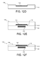
- the Figures 12A to 12F represent the steps of a method for producing the encapsulation structure 100 according to the first embodiment, that is to say in which the cover 106 is made by substrate transfer.
- the micro-device 104 is first made in the substrate 102 by the implementation of conventional steps of microelectronics (deposition, photolithography, etching, etc.).
- the cover 106 is then made from a layer 112 corresponding to a substrate, or wafer, for example glass or silicon ( figure 12B ).
- a depression 132 for forming at least a portion of the cavity 110 of the encapsulation structure 100 is etched in the layer 112, thus revealing the face 114 of the layer 112 which will form the upper wall of the cavity 110 ( figure 12C ).
- the mechanical reinforcing portions 116 are then made against the face 114, in the hollow 132 ( figure 12D ).
- These mechanical reinforcing portions 116 are for example made via a first PVD deposition of a titanium or chromium tie layer having a thickness equal to a few tens of nanometers, followed by the deposition of a second nickel-silver barrier layer. thickness equal to a few hundred nanometers, and finally the deposition of a third layer of Au thickness equal to a few tens of nanometers. These three deposited layers form the seed layer, corresponding to the first layer 118.
- the material of the second layer 120 of the mechanical reinforcing portions 116 is then deposited by ECD with a thickness as described above, ranging from several microns to several tens microns.
- This deposit is for example made through patterns made in a photosensitive film disposed above the seed layer.
- Several layers of material may be deposited through this film, ending in particular by the deposition of a metal getter material so that it is found exposed in the cavity 110.
- the material or materials deposited between the portions 116, on the film photosensitive, can be removed simultaneously with this film by lift-off.
- the portions of the seed layer between the mechanical reinforcing portions 116 are then etched, for example chemically. Prior to this etching, it is possible to protect the mechanical reinforcing portions 116, and especially the getter material, by nitriding or dry oxidation of this or these materials, thus limiting the chemical etching of this or these materials during chemical etching of the seed layer.
- the material of the mechanical reinforcing portions 116 is not removable by ECD, this material can be deposited by PVD.
- the different layers of the mechanical reinforcing portions 116 are firstly deposited, then the mechanical reinforcing portions 116 are obtained by shaping these layers, for example via a photolithography and lift-off or an etching chemical of these layers.
- the cover 106 thus obtained is then secured to the substrate 102, directly or via a sealing bead according to the nature of the materials of the layer 112 and the substrate 102.
- the micro-device 104 is then encapsulated in the cavity 110 in which are the mechanical reinforcing portions 116 at the upper wall of the cavity 110 ( figure 12E ).
- the encapsulation structure 100 is completed by thinning the layer 112.
- the cover 106 comprising the layer 112 and the mechanical reinforcing portions 106
- the cover 106 can be made first in a mold corresponding for example to an etched substrate of glass or silicon.
- the substrate intended to serve as a mold is first etched in the desired shape of the cover 106.
- a polymer layer, for example PTFE, is deposited on the etched face of the mold.
- the layers intended to form the cap 106, that is to say the layer 112 and the layer or layers of the mechanical reinforcing portions 116, are then deposited on the polymer layer, for example via steps similar to those previously described. in connection with the figure 12D .
- the cover 106 made in the mold is then assembled to the substrate comprising the micro-device to be encapsulated by transferring the mold to the substrate and secured to the substrate, for example via a polymer bonding, or by eutectic melting or by thermocompression.
- the mold is finally detached from the cap 106 via the removal of the polymer layer to form the encapsulation structure. Details of implementation of such a method are for example described in the documents FR 2 934 580 and US 7,897,436 .
Landscapes
- Engineering & Computer Science (AREA)
- Microelectronics & Electronic Packaging (AREA)
- Manufacturing & Machinery (AREA)
- Computer Hardware Design (AREA)
- Health & Medical Sciences (AREA)
- General Health & Medical Sciences (AREA)
- Toxicology (AREA)
- Mechanical Engineering (AREA)
- Micromachines (AREA)
- Laminated Bodies (AREA)
Applications Claiming Priority (1)
| Application Number | Priority Date | Filing Date | Title |
|---|---|---|---|
| FR1357386A FR3008965B1 (fr) | 2013-07-26 | 2013-07-26 | Structure d'encapsulation comprenant un capot renforce mecaniquement et a effet getter |
Publications (3)
| Publication Number | Publication Date |
|---|---|
| EP2829508A2 true EP2829508A2 (de) | 2015-01-28 |
| EP2829508A3 EP2829508A3 (de) | 2015-04-08 |
| EP2829508B1 EP2829508B1 (de) | 2020-03-11 |
Family
ID=49713179
Family Applications (1)
| Application Number | Title | Priority Date | Filing Date |
|---|---|---|---|
| EP14178068.4A Active EP2829508B1 (de) | 2013-07-26 | 2014-07-22 | Einkapselungsstruktur, die eine mechanisch verstärkte Hülle mit Getter-Effekt umfasst |
Country Status (4)
| Country | Link |
|---|---|
| US (1) | US9511991B2 (de) |
| EP (1) | EP2829508B1 (de) |
| CN (1) | CN104340948B (de) |
| FR (1) | FR3008965B1 (de) |
Families Citing this family (23)
| Publication number | Priority date | Publication date | Assignee | Title |
|---|---|---|---|---|
| FR2985602B1 (fr) | 2012-01-05 | 2014-03-07 | Commissariat Energie Atomique | Procede de gravure d'un motif complexe |
| FR3014241B1 (fr) | 2013-11-29 | 2017-05-05 | Commissariat Energie Atomique | Structure d'encapsulation comprenant des tranchees partiellement remplies de materiau getter |
| DK3077110T3 (da) * | 2013-12-06 | 2019-08-19 | Univ Danmarks Tekniske | Katalysator til ammoniakoxidation |
| FR3018916B1 (fr) | 2014-03-19 | 2017-08-25 | Commissariat Energie Atomique | Capteur de mesure de pression differentielle microelectromecanique et/ou nanoelectromecanique |
| FR3021645B1 (fr) | 2014-06-03 | 2019-06-14 | Commissariat A L'energie Atomique Et Aux Energies Alternatives | Structure d'encapsulation a plusieurs cavites munies de canaux d'acces de hauteurs differentes |
| FR3021814B1 (fr) | 2014-08-08 | 2018-06-15 | Commissariat Energie Atomique | Connecteur pour la connexion en matrice entre un boitier et un support, comportant un corps principal plie |
| FR3026560B1 (fr) | 2014-09-30 | 2016-10-28 | Commissariat Energie Atomique | Structure d'encapsulation pourvue d'un capot et d'un substrat, pour connecter au moins un nano-objet sur une face du substrat et en reprendre le contact au travers du capot, et procede de fabrication de la structure |
| FR3027380A1 (fr) * | 2014-10-17 | 2016-04-22 | Commissariat Energie Atomique | Dispositif de refroidissement par liquide caloporteur pour composants electroniques |
| DE102015102869B4 (de) * | 2015-02-27 | 2017-05-11 | Snaptrack, Inc. | MEMS-Bauelement mit hoher Integrationsdichte und Verfahren zu seiner Herstellung |
| DE102015114248B4 (de) | 2015-08-27 | 2019-01-17 | Marcel P. HOFSAESS | Temperaturabhängiger Schalter mit Schneidgrat |
| US9550667B1 (en) | 2015-09-08 | 2017-01-24 | Taiwan Semiconductor Manufactruing Company Ltd. | Semiconductor structure and manufacturing method thereof |
| US10689249B2 (en) * | 2015-09-16 | 2020-06-23 | Advanced Semiconductor Engineering, Inc. | Semiconductor device package including a wall and a grounding ring exposed from the wall |
| US10442683B2 (en) * | 2016-04-14 | 2019-10-15 | Akustica, Inc. | Corrugated package for microelectromechanical system (MEMS) device |
| FR3050870B1 (fr) * | 2016-04-28 | 2018-05-25 | Commissariat A L'energie Atomique Et Aux Energies Alternatives | Procede de realisation d’un dispositif de detection de rayonnement electromagnetique comportant une couche en un materiau getter |
| GB2557717A (en) * | 2016-10-12 | 2018-06-27 | Cirrus Logic Int Semiconductor Ltd | Transducer packaging |
| FR3063992B1 (fr) * | 2017-03-16 | 2021-07-16 | Commissariat Energie Atomique | Micro-dispositif comprenant au moins un element mobile |
| FR3070096B1 (fr) * | 2017-08-08 | 2021-09-17 | Commissariat Energie Atomique | Procede de fabrication d'un dispositif de detection a deux substrats et un tel dispositif de detection |
| JP2020161520A (ja) * | 2019-03-25 | 2020-10-01 | ソニーセミコンダクタソリューションズ株式会社 | 撮像装置 |
| US11094649B2 (en) * | 2020-01-21 | 2021-08-17 | Advanced Semiconductor Engineering, Inc. | Semiconductor package structure and method for manufacturing the same |
| US11482449B2 (en) * | 2020-08-03 | 2022-10-25 | General Electric Company | Electrical component with a dielectric passivation stack |
| CN116022727B (zh) * | 2021-10-27 | 2026-02-03 | 上海新微技术研发中心有限公司 | 吸气剂薄膜结构的制造方法 |
| CN116022726B (zh) * | 2021-10-27 | 2026-02-03 | 上海新微技术研发中心有限公司 | 复合吸气剂薄膜结构的制造方法 |
| EP4526922A4 (de) * | 2022-05-16 | 2026-04-29 | Mesoline Inc | Gettersysteme für die mikroelektronik und herstellungsverfahren dafür |
Citations (5)
| Publication number | Priority date | Publication date | Assignee | Title |
|---|---|---|---|---|
| FR2901264A1 (fr) | 2006-05-22 | 2007-11-23 | Commissariat Energie Atomique | Microcomposant muni d'une cavite delimitee par un capot a resistance mecanique amelioree |
| FR2922202A1 (fr) | 2007-10-15 | 2009-04-17 | Commissariat Energie Atomique | Structure comportant une couche getter et une sous-couche d'ajustement et procede de fabrication. |
| FR2934580A1 (fr) | 2008-08-01 | 2010-02-05 | Kfm Technology | Procede et dispositif d'encapsulation de microstructures |
| US7897436B2 (en) | 2004-11-26 | 2011-03-01 | Stmicroelectronics, S.A. | Process for packaging micro-components using a matrix |
| FR2955999A1 (fr) | 2010-02-04 | 2011-08-05 | Commissariat Energie Atomique | Procede d'encapsulation d'un microcomposant par un capot renforce mecaniquement |
Family Cites Families (12)
| Publication number | Priority date | Publication date | Assignee | Title |
|---|---|---|---|---|
| US5268533A (en) * | 1991-05-03 | 1993-12-07 | Hughes Aircraft Company | Pre-stressed laminated lid for electronic circuit package |
| US6992375B2 (en) * | 2000-11-30 | 2006-01-31 | Texas Instruments Incorporated | Anchor for device package |
| ITMI20030069A1 (it) * | 2003-01-17 | 2004-07-18 | Getters Spa | Dispositivi micromeccanici o microoptoelettronici con deposito di materiale getter e riscaldatore integrato. |
| US7492019B2 (en) | 2003-03-07 | 2009-02-17 | Ic Mechanics, Inc. | Micromachined assembly with a multi-layer cap defining a cavity |
| US7204737B2 (en) * | 2004-09-23 | 2007-04-17 | Temic Automotive Of North America, Inc. | Hermetically sealed microdevice with getter shield |
| US7368803B2 (en) * | 2004-09-27 | 2008-05-06 | Idc, Llc | System and method for protecting microelectromechanical systems array using back-plate with non-flat portion |
| FR2875948B1 (fr) | 2004-09-28 | 2006-12-08 | Commissariat Energie Atomique | Composant d'encapsulation de micro-systeme electromecaniques integres et procede de realisation du composant |
| US7462931B2 (en) * | 2006-05-15 | 2008-12-09 | Innovative Micro Technology | Indented structure for encapsulated devices and method of manufacture |
| US7923790B1 (en) * | 2007-03-09 | 2011-04-12 | Silicon Laboratories Inc. | Planar microshells for vacuum encapsulated devices and damascene method of manufacture |
| EP2008966A3 (de) * | 2007-06-27 | 2013-06-12 | Sumitomo Precision Products Co., Ltd. | In einer hermetischen Kammer mit einem Getterfilm geformte MEMS-Vorrichtung |
| US20120106085A1 (en) * | 2009-02-19 | 2012-05-03 | Takao Yamazaki | Vacuum sealed package, printed circuit board having vacuum sealed package, electronic device, and method for manufacturing vacuum sealed package |
| FR2985602B1 (fr) | 2012-01-05 | 2014-03-07 | Commissariat Energie Atomique | Procede de gravure d'un motif complexe |
-
2013
- 2013-07-26 FR FR1357386A patent/FR3008965B1/fr not_active Expired - Fee Related
-
2014
- 2014-07-15 US US14/331,285 patent/US9511991B2/en active Active
- 2014-07-22 EP EP14178068.4A patent/EP2829508B1/de active Active
- 2014-07-28 CN CN201410364783.1A patent/CN104340948B/zh active Active
Patent Citations (5)
| Publication number | Priority date | Publication date | Assignee | Title |
|---|---|---|---|---|
| US7897436B2 (en) | 2004-11-26 | 2011-03-01 | Stmicroelectronics, S.A. | Process for packaging micro-components using a matrix |
| FR2901264A1 (fr) | 2006-05-22 | 2007-11-23 | Commissariat Energie Atomique | Microcomposant muni d'une cavite delimitee par un capot a resistance mecanique amelioree |
| FR2922202A1 (fr) | 2007-10-15 | 2009-04-17 | Commissariat Energie Atomique | Structure comportant une couche getter et une sous-couche d'ajustement et procede de fabrication. |
| FR2934580A1 (fr) | 2008-08-01 | 2010-02-05 | Kfm Technology | Procede et dispositif d'encapsulation de microstructures |
| FR2955999A1 (fr) | 2010-02-04 | 2011-08-05 | Commissariat Energie Atomique | Procede d'encapsulation d'un microcomposant par un capot renforce mecaniquement |
Also Published As
| Publication number | Publication date |
|---|---|
| EP2829508A3 (de) | 2015-04-08 |
| CN104340948A (zh) | 2015-02-11 |
| EP2829508B1 (de) | 2020-03-11 |
| FR3008965A1 (fr) | 2015-01-30 |
| US9511991B2 (en) | 2016-12-06 |
| US20150028433A1 (en) | 2015-01-29 |
| FR3008965B1 (fr) | 2017-03-03 |
| CN104340948B (zh) | 2018-02-27 |
Similar Documents
| Publication | Publication Date | Title |
|---|---|---|
| EP2829508B1 (de) | Einkapselungsstruktur, die eine mechanisch verstärkte Hülle mit Getter-Effekt umfasst | |
| EP2450949B1 (de) | Einkapselungssstruktur einer Mikrovorrichtung, die ein Getter-Material umfasst | |
| EP2284121B1 (de) | Hohlraum für ein mikromechanisches Bauelement | |
| EP2308797B1 (de) | Struktur mit Hohlraum, die eine Bindungsschnittstelle auf der Basis eines Getter-Materials umfasst | |
| EP2952471B1 (de) | Verkapselungsstruktur mit mehreren hohlräumen versehen mit zugangskanälen unterschiedlicher höhe | |
| EP2354083B1 (de) | Verpackungsverfahren für mikromechanisches Bauteil mit mechanisch verstärkter Kappe | |
| EP2423160B1 (de) | Verbindung von Gegenständen mittels einer Versiegelungsnaht, die intermetallische Verbindungen umfasst | |
| EP2637966B1 (de) | Verfahren zur herstellung eines substrats mit eingebetteten schichten aus fangstoff | |
| FR2933390A1 (fr) | Procede d'encapsulation d'un dispositif microelectronique par un materiau getter | |
| FR2941532A1 (fr) | Dispositif de capteur et son procede de fabrication | |
| EP2897162B1 (de) | Einkapselungsstruktur, die teilweise mit Gettermaterial gefüllte Rinnen umfasst | |
| EP2019811A1 (de) | Mit einem durch eine kappe mit verbesserter mechanischer festigkeit begrenzten hohlraum versehene mikrokomponente | |
| EP2586741B1 (de) | Hermetisch verschlossene Einkapselungsstruktur einer Vorrichtung und einer elektronischen Komponente | |
| EP3034460B1 (de) | Mehrstufige getter-struktur und einkapselungsstruktur, die eine solche mehrstufige getter-struktur umfasst | |
| EP3184486B1 (de) | Verfahren zur herstellung eines versiegelten mems-hohlraums mit einer klappe zum schützen des hohlraums während des verkapselungsvorgangs | |
| EP1932804B1 (de) | Silizium-Metall-Mischteile und damit verbundene Herstellungsverfahren | |
| EP2791969B1 (de) | Herstellung einer elektrischen durchgangsverbindung | |
| EP3165502B1 (de) | Mikroelektronische vorrichtung | |
| EP3173375B1 (de) | Einkapselungsverfahren einer mikroelektronischen vorrichtung mit einem auslassloch variabler grösse | |
| EP1557394B1 (de) | Vorrichtung und Verfahren zur Sicherung der Dichtheit eines Hohlraumes, in die eine Durchführungsöffnung mündet | |
| FR2970116A1 (fr) | Procede d'encapsulation d'un microcomposant | |
| WO2008012481A1 (fr) | Procédé de fabrication d'un circuit intégré encapsulé et circuit intégré encapsulé associé | |
| CH705797A2 (fr) | Dispositif d'encapsulage et procédé de fabrication d'un tel dispositif d'encapsulage. |
Legal Events
| Date | Code | Title | Description |
|---|---|---|---|
| 17P | Request for examination filed |
Effective date: 20140722 |
|
| AK | Designated contracting states |
Kind code of ref document: A2 Designated state(s): AL AT BE BG CH CY CZ DE DK EE ES FI FR GB GR HR HU IE IS IT LI LT LU LV MC MK MT NL NO PL PT RO RS SE SI SK SM TR |
|
| AX | Request for extension of the european patent |
Extension state: BA ME |
|
| PUAI | Public reference made under article 153(3) epc to a published international application that has entered the european phase |
Free format text: ORIGINAL CODE: 0009012 |
|
| PUAL | Search report despatched |
Free format text: ORIGINAL CODE: 0009013 |
|
| AK | Designated contracting states |
Kind code of ref document: A3 Designated state(s): AL AT BE BG CH CY CZ DE DK EE ES FI FR GB GR HR HU IE IS IT LI LT LU LV MC MK MT NL NO PL PT RO RS SE SI SK SM TR |
|
| AX | Request for extension of the european patent |
Extension state: BA ME |
|
| RIC1 | Information provided on ipc code assigned before grant |
Ipc: B81B 3/00 20060101AFI20150305BHEP |
|
| R17P | Request for examination filed (corrected) |
Effective date: 20150810 |
|
| RBV | Designated contracting states (corrected) |
Designated state(s): AL AT BE BG CH CY CZ DE DK EE ES FI FR GB GR HR HU IE IS IT LI LT LU LV MC MK MT NL NO PL PT RO RS SE SI SK SM TR |
|
| STAA | Information on the status of an ep patent application or granted ep patent |
Free format text: STATUS: EXAMINATION IS IN PROGRESS |
|
| 17Q | First examination report despatched |
Effective date: 20181024 |
|
| GRAP | Despatch of communication of intention to grant a patent |
Free format text: ORIGINAL CODE: EPIDOSNIGR1 |
|
| STAA | Information on the status of an ep patent application or granted ep patent |
Free format text: STATUS: GRANT OF PATENT IS INTENDED |
|
| INTG | Intention to grant announced |
Effective date: 20191014 |
|
| GRAS | Grant fee paid |
Free format text: ORIGINAL CODE: EPIDOSNIGR3 |
|
| GRAA | (expected) grant |
Free format text: ORIGINAL CODE: 0009210 |
|
| STAA | Information on the status of an ep patent application or granted ep patent |
Free format text: STATUS: THE PATENT HAS BEEN GRANTED |
|
| AK | Designated contracting states |
Kind code of ref document: B1 Designated state(s): AL AT BE BG CH CY CZ DE DK EE ES FI FR GB GR HR HU IE IS IT LI LT LU LV MC MK MT NL NO PL PT RO RS SE SI SK SM TR |
|
| REG | Reference to a national code |
Ref country code: GB Ref legal event code: FG4D Free format text: NOT ENGLISH |
|
| REG | Reference to a national code |
Ref country code: CH Ref legal event code: EP |
|
| REG | Reference to a national code |
Ref country code: AT Ref legal event code: REF Ref document number: 1242922 Country of ref document: AT Kind code of ref document: T Effective date: 20200315 |
|
| REG | Reference to a national code |
Ref country code: DE Ref legal event code: R096 Ref document number: 602014062081 Country of ref document: DE |
|
| REG | Reference to a national code |
Ref country code: IE Ref legal event code: FG4D Free format text: LANGUAGE OF EP DOCUMENT: FRENCH |
|
| PG25 | Lapsed in a contracting state [announced via postgrant information from national office to epo] |
Ref country code: RS Free format text: LAPSE BECAUSE OF FAILURE TO SUBMIT A TRANSLATION OF THE DESCRIPTION OR TO PAY THE FEE WITHIN THE PRESCRIBED TIME-LIMIT Effective date: 20200311 Ref country code: FI Free format text: LAPSE BECAUSE OF FAILURE TO SUBMIT A TRANSLATION OF THE DESCRIPTION OR TO PAY THE FEE WITHIN THE PRESCRIBED TIME-LIMIT Effective date: 20200311 Ref country code: NO Free format text: LAPSE BECAUSE OF FAILURE TO SUBMIT A TRANSLATION OF THE DESCRIPTION OR TO PAY THE FEE WITHIN THE PRESCRIBED TIME-LIMIT Effective date: 20200611 |
|
| REG | Reference to a national code |
Ref country code: NL Ref legal event code: MP Effective date: 20200311 |
|
| PG25 | Lapsed in a contracting state [announced via postgrant information from national office to epo] |
Ref country code: LV Free format text: LAPSE BECAUSE OF FAILURE TO SUBMIT A TRANSLATION OF THE DESCRIPTION OR TO PAY THE FEE WITHIN THE PRESCRIBED TIME-LIMIT Effective date: 20200311 Ref country code: SE Free format text: LAPSE BECAUSE OF FAILURE TO SUBMIT A TRANSLATION OF THE DESCRIPTION OR TO PAY THE FEE WITHIN THE PRESCRIBED TIME-LIMIT Effective date: 20200311 Ref country code: HR Free format text: LAPSE BECAUSE OF FAILURE TO SUBMIT A TRANSLATION OF THE DESCRIPTION OR TO PAY THE FEE WITHIN THE PRESCRIBED TIME-LIMIT Effective date: 20200311 Ref country code: BG Free format text: LAPSE BECAUSE OF FAILURE TO SUBMIT A TRANSLATION OF THE DESCRIPTION OR TO PAY THE FEE WITHIN THE PRESCRIBED TIME-LIMIT Effective date: 20200611 Ref country code: GR Free format text: LAPSE BECAUSE OF FAILURE TO SUBMIT A TRANSLATION OF THE DESCRIPTION OR TO PAY THE FEE WITHIN THE PRESCRIBED TIME-LIMIT Effective date: 20200612 |
|
| REG | Reference to a national code |
Ref country code: LT Ref legal event code: MG4D |
|
| PG25 | Lapsed in a contracting state [announced via postgrant information from national office to epo] |
Ref country code: NL Free format text: LAPSE BECAUSE OF FAILURE TO SUBMIT A TRANSLATION OF THE DESCRIPTION OR TO PAY THE FEE WITHIN THE PRESCRIBED TIME-LIMIT Effective date: 20200311 |
|
| PG25 | Lapsed in a contracting state [announced via postgrant information from national office to epo] |
Ref country code: LT Free format text: LAPSE BECAUSE OF FAILURE TO SUBMIT A TRANSLATION OF THE DESCRIPTION OR TO PAY THE FEE WITHIN THE PRESCRIBED TIME-LIMIT Effective date: 20200311 Ref country code: SK Free format text: LAPSE BECAUSE OF FAILURE TO SUBMIT A TRANSLATION OF THE DESCRIPTION OR TO PAY THE FEE WITHIN THE PRESCRIBED TIME-LIMIT Effective date: 20200311 Ref country code: IS Free format text: LAPSE BECAUSE OF FAILURE TO SUBMIT A TRANSLATION OF THE DESCRIPTION OR TO PAY THE FEE WITHIN THE PRESCRIBED TIME-LIMIT Effective date: 20200711 Ref country code: PT Free format text: LAPSE BECAUSE OF FAILURE TO SUBMIT A TRANSLATION OF THE DESCRIPTION OR TO PAY THE FEE WITHIN THE PRESCRIBED TIME-LIMIT Effective date: 20200805 Ref country code: CZ Free format text: LAPSE BECAUSE OF FAILURE TO SUBMIT A TRANSLATION OF THE DESCRIPTION OR TO PAY THE FEE WITHIN THE PRESCRIBED TIME-LIMIT Effective date: 20200311 Ref country code: RO Free format text: LAPSE BECAUSE OF FAILURE TO SUBMIT A TRANSLATION OF THE DESCRIPTION OR TO PAY THE FEE WITHIN THE PRESCRIBED TIME-LIMIT Effective date: 20200311 Ref country code: SM Free format text: LAPSE BECAUSE OF FAILURE TO SUBMIT A TRANSLATION OF THE DESCRIPTION OR TO PAY THE FEE WITHIN THE PRESCRIBED TIME-LIMIT Effective date: 20200311 Ref country code: EE Free format text: LAPSE BECAUSE OF FAILURE TO SUBMIT A TRANSLATION OF THE DESCRIPTION OR TO PAY THE FEE WITHIN THE PRESCRIBED TIME-LIMIT Effective date: 20200311 |
|
| REG | Reference to a national code |
Ref country code: AT Ref legal event code: MK05 Ref document number: 1242922 Country of ref document: AT Kind code of ref document: T Effective date: 20200311 |
|
| REG | Reference to a national code |
Ref country code: DE Ref legal event code: R097 Ref document number: 602014062081 Country of ref document: DE |
|
| PLBE | No opposition filed within time limit |
Free format text: ORIGINAL CODE: 0009261 |
|
| STAA | Information on the status of an ep patent application or granted ep patent |
Free format text: STATUS: NO OPPOSITION FILED WITHIN TIME LIMIT |
|
| PG25 | Lapsed in a contracting state [announced via postgrant information from national office to epo] |
Ref country code: ES Free format text: LAPSE BECAUSE OF FAILURE TO SUBMIT A TRANSLATION OF THE DESCRIPTION OR TO PAY THE FEE WITHIN THE PRESCRIBED TIME-LIMIT Effective date: 20200311 Ref country code: DK Free format text: LAPSE BECAUSE OF FAILURE TO SUBMIT A TRANSLATION OF THE DESCRIPTION OR TO PAY THE FEE WITHIN THE PRESCRIBED TIME-LIMIT Effective date: 20200311 Ref country code: AT Free format text: LAPSE BECAUSE OF FAILURE TO SUBMIT A TRANSLATION OF THE DESCRIPTION OR TO PAY THE FEE WITHIN THE PRESCRIBED TIME-LIMIT Effective date: 20200311 |
|
| 26N | No opposition filed |
Effective date: 20201214 |
|
| PG25 | Lapsed in a contracting state [announced via postgrant information from national office to epo] |
Ref country code: SI Free format text: LAPSE BECAUSE OF FAILURE TO SUBMIT A TRANSLATION OF THE DESCRIPTION OR TO PAY THE FEE WITHIN THE PRESCRIBED TIME-LIMIT Effective date: 20200311 Ref country code: PL Free format text: LAPSE BECAUSE OF FAILURE TO SUBMIT A TRANSLATION OF THE DESCRIPTION OR TO PAY THE FEE WITHIN THE PRESCRIBED TIME-LIMIT Effective date: 20200311 Ref country code: MC Free format text: LAPSE BECAUSE OF FAILURE TO SUBMIT A TRANSLATION OF THE DESCRIPTION OR TO PAY THE FEE WITHIN THE PRESCRIBED TIME-LIMIT Effective date: 20200311 |
|
| REG | Reference to a national code |
Ref country code: CH Ref legal event code: PL |
|
| REG | Reference to a national code |
Ref country code: BE Ref legal event code: MM Effective date: 20200731 |
|
| PG25 | Lapsed in a contracting state [announced via postgrant information from national office to epo] |
Ref country code: LU Free format text: LAPSE BECAUSE OF NON-PAYMENT OF DUE FEES Effective date: 20200722 Ref country code: LI Free format text: LAPSE BECAUSE OF NON-PAYMENT OF DUE FEES Effective date: 20200731 Ref country code: CH Free format text: LAPSE BECAUSE OF NON-PAYMENT OF DUE FEES Effective date: 20200731 |
|
| PG25 | Lapsed in a contracting state [announced via postgrant information from national office to epo] |
Ref country code: BE Free format text: LAPSE BECAUSE OF NON-PAYMENT OF DUE FEES Effective date: 20200731 |
|
| PG25 | Lapsed in a contracting state [announced via postgrant information from national office to epo] |
Ref country code: IE Free format text: LAPSE BECAUSE OF NON-PAYMENT OF DUE FEES Effective date: 20200722 |
|
| PG25 | Lapsed in a contracting state [announced via postgrant information from national office to epo] |
Ref country code: TR Free format text: LAPSE BECAUSE OF FAILURE TO SUBMIT A TRANSLATION OF THE DESCRIPTION OR TO PAY THE FEE WITHIN THE PRESCRIBED TIME-LIMIT Effective date: 20200311 Ref country code: MT Free format text: LAPSE BECAUSE OF FAILURE TO SUBMIT A TRANSLATION OF THE DESCRIPTION OR TO PAY THE FEE WITHIN THE PRESCRIBED TIME-LIMIT Effective date: 20200311 Ref country code: CY Free format text: LAPSE BECAUSE OF FAILURE TO SUBMIT A TRANSLATION OF THE DESCRIPTION OR TO PAY THE FEE WITHIN THE PRESCRIBED TIME-LIMIT Effective date: 20200311 |
|
| PG25 | Lapsed in a contracting state [announced via postgrant information from national office to epo] |
Ref country code: MK Free format text: LAPSE BECAUSE OF FAILURE TO SUBMIT A TRANSLATION OF THE DESCRIPTION OR TO PAY THE FEE WITHIN THE PRESCRIBED TIME-LIMIT Effective date: 20200311 Ref country code: AL Free format text: LAPSE BECAUSE OF FAILURE TO SUBMIT A TRANSLATION OF THE DESCRIPTION OR TO PAY THE FEE WITHIN THE PRESCRIBED TIME-LIMIT Effective date: 20200311 |
|
| PGFP | Annual fee paid to national office [announced via postgrant information from national office to epo] |
Ref country code: DE Payment date: 20250722 Year of fee payment: 12 |
|
| PGFP | Annual fee paid to national office [announced via postgrant information from national office to epo] |
Ref country code: IT Payment date: 20250731 Year of fee payment: 12 |
|
| PGFP | Annual fee paid to national office [announced via postgrant information from national office to epo] |
Ref country code: GB Payment date: 20250724 Year of fee payment: 12 |
|
| PGFP | Annual fee paid to national office [announced via postgrant information from national office to epo] |
Ref country code: FR Payment date: 20250722 Year of fee payment: 12 |