EP2830228B1 - HF-Vorrichtung und Verfahren mit verbesserter aktiver Belastungsmodulationskapazität - Google Patents
HF-Vorrichtung und Verfahren mit verbesserter aktiver Belastungsmodulationskapazität Download PDFInfo
- Publication number
- EP2830228B1 EP2830228B1 EP13177543.9A EP13177543A EP2830228B1 EP 2830228 B1 EP2830228 B1 EP 2830228B1 EP 13177543 A EP13177543 A EP 13177543A EP 2830228 B1 EP2830228 B1 EP 2830228B1
- Authority
- EP
- European Patent Office
- Prior art keywords
- circuit
- resonance
- resonance circuit
- transmission mode
- resonance frequency
- Prior art date
- Legal status (The legal status is an assumption and is not a legal conclusion. Google has not performed a legal analysis and makes no representation as to the accuracy of the status listed.)
- Active
Links
Images


Classifications
-
- H—ELECTRICITY
- H04—ELECTRIC COMMUNICATION TECHNIQUE
- H04B—TRANSMISSION
- H04B5/00—Near-field transmission systems, e.g. inductive or capacitive transmission systems
- H04B5/20—Near-field transmission systems, e.g. inductive or capacitive transmission systems characterised by the transmission technique; characterised by the transmission medium
- H04B5/24—Inductive coupling
-
- H—ELECTRICITY
- H04—ELECTRIC COMMUNICATION TECHNIQUE
- H04B—TRANSMISSION
- H04B1/00—Details of transmission systems, not covered by a single one of groups H04B3/00 - H04B13/00; Details of transmission systems not characterised by the medium used for transmission
- H04B1/38—Transceivers, i.e. devices in which transmitter and receiver form a structural unit and in which at least one part is used for functions of transmitting and receiving
- H04B1/40—Circuits
- H04B1/44—Transmit/receive switching
-
- H—ELECTRICITY
- H04—ELECTRIC COMMUNICATION TECHNIQUE
- H04B—TRANSMISSION
- H04B5/00—Near-field transmission systems, e.g. inductive or capacitive transmission systems
- H04B5/40—Near-field transmission systems, e.g. inductive or capacitive transmission systems characterised by components specially adapted for near-field transmission
- H04B5/48—Transceivers
Definitions
- the present invention relates to the field of RF devices, in particular to RF devices for short range or contactless communication using active load modulation.
- Recent RF devices such as contactless transponder cards (e.g. Smartcards, e-Passports, Tickets, etc.) and NFC (Near Field Communication) devices, are capable of performing half-duplex bi-directional communication with a reader device.
- these RF devices are capable of operating in a receiving mode as well as in a transmitting mode.
- RF devices may utilize active load modulation to transmit the information or data.
- the antenna circuit of the RF device is tuned to the carrier frequency of the reader device, e.g. to 13.56 MHz in systems complying with ISO/IEC 14443 and NFC standards.
- such an antenna configuration is usually not ideal for use in the receiving mode, as the shape of the reader modulation may experience a negative impact.
- an antenna configuration optimized for the receiving mode is usually not ideal for use in the transmitting mode.
- an RF bidirectional communication device utilizing active load modulation, the device comprising (a) a resonance circuit including an antenna, and (b) a control unit for controlling communication of the device, including switching between a transmission mode and a receiving mode, wherein the control unit is adapted to (c) modify a configuration of the resonance circuit such that the resonance circuit has a first resonance frequency when the device is in the receiving mode and a second resonance frequency when the device is in the transmission mode, and (d) modify the configuration of the resonance circuit such that a Q-factor of the resonance circuit is periodically modified while the device is in the transmission mode.
- This aspect is based on the idea that the resonance frequency and the Q-factor of the resonance circuit are optimized to either of the transmission mode and the receiving mode.
- the second resonance frequency By choosing the second resonance frequency to be equal to the carrier frequency of a corresponding reader/writer device, a relatively high Q-factor can be obtained such that transmission can take place efficiently. More specifically, the high Q-factor allows greater output power for the side-band levels and thereby a high LMA (load modulation amplitude).
- a different resonance frequency in the receiving mode i.e. the first resonance frequency
- reception can be optimized as a lower Q-factor provides a greater bandwidth which is beneficial for reception as the received signal is less influenced.
- this aspect is based on the idea that by periodically modifying the Q-factor of the resonance circuit while the device is in the transmission mode, the long time for settling of the voltages at the antenna network caused by the high Q-factor can be countered. More specifically, by periodically modifying the Q-factor within the modulation pauses during transmission, the antenna circuit is forced back to its idle condition within a short period.
- Q-factor denotes the “quality factor”, also known in the art simply as "Q”, which characterizes the bandwidth of the resonance circuit relative to its resonance frequency.
- modifying the Q-factor may particularly denote increasing and/or decreasing the Q-factor.
- configuration of the resonance circuit may particularly denote the physical configuration of the electrical components that form the resonance circuit.
- the RF bidirectional communication device may in particular be a contactless transponder card or an NFC device.
- the control unit may comprise a processor and program memory loaded with control programs. Alternatively or additionally, the control unit may comprise dedicated hardwired logic. In any case, the control unit is capable of controlling various communication functions of the device. In particular, the control unit may modify the configuration of the resonance circuit by controlling respective switches such that various electronic components are connected or disconnected from the resonance circuit, thereby changing the resonance frequency and/or Q-factor of the resonance circuit.
- the switches may be comprised by the control unit or they may be separate from the control unit. In the latter case, the switches are connected to the control unit such that the control unit may control the state of the switches by transmitting corresponding control signals to a control terminal of each switch.
- the resonance circuit comprises a switchable capacitive circuit
- the control unit is adapted to modify the configuration of the resonance circuit by selectively connecting and disconnecting the switchable capacitive circuit.
- the switchable capacitor circuit may comprise one or more capacitors which may be individually connected and disconnected from the resonance circuit by the control unit. Thereby, by changing the configuration of capacitors in the resonance circuit, the resonance frequency can be changed accordingly.
- control unit is adapted to connect the switchable capacitive circuit when switching from the receiving mode to the transmission mode and to disconnect the switchable capacitive circuit when switching from the transmission mode to the receiving mode.
- the switchable capacitive circuit is part of the resonance circuit when the device is operating in the transmission mode, whereas the switchable capacitive circuit is not part of, i.e. disconnected from the resonance circuit when the device is operating in the receiving mode.
- the above refers to a case where the first resonance frequency is higher than the second resonance frequency.
- the switchable capacitive circuit would be part of the resonance circuit when the device is operating in the receiving mode and disconnected when the device is operating in the transmission mode.
- the first resonance frequency is larger or smaller than the second resonance frequency.
- the switchable capacitive circuit may in particular be achieved by designing the switchable capacitive circuit such that it constitutes a capacitor arranged in parallel with the antenna when the switchable capacitive is connected to the resonance circuit.
- the resonance frequency of the resonance circuit will increase when the switchable capacitive circuit is disconnected, i.e. when the total capacitance arranged in parallel with the antenna is reduced.
- the resonance circuit comprises an adjustable resistive circuit, wherein the control unit is adapted to adjust the resistance of the resistive circuit in an alternating manner when the device is in the transmission mode.
- the adjustable resistive circuit may be constituted by at least one resistor and is arranged in such a way that it influences the total resistance of the antenna circuit.
- the Q-factor of the resonance circuit will alternate between a higher value and a lower value. More specifically, when the resistance of the adjustable resistive circuit is increased, the Q-factor is reduced, and when the resistance of the adjustable resistive circuit is reduced, the Q-factor is increased.
- the above mentioned advantageous effect that the long time for settling of the voltages at the antenna network caused by the high Q-factor can be countered may be obtained in a simple and cost efficient way.
- the antenna circuit is forced back to its idle condition within a short period.
- the first resonance frequency is 14.4075 MHz and/or the second resonance frequency is 13.56 MHz.
- first and second resonance frequencies will allow the device to operate in accordance with devices complying with e.g. the NFC standard. It is noted that other frequency values may be selected depending on the circumstances.
- a method of performing bidirectional communication between an RF device and a reader/writer device comprising (a) setting the RF device to operate in a receiving mode by configuring a resonance circuit of the RF device to have a first resonance frequency, the resonance circuit including an antenna, (b) receiving, at the RF device, a request for transmission from the reader/writer device, (c) setting the RF device to operate in a transmission mode by configuring the resonance circuit of the RF device to have a second resonance frequency, and (d) during operation in the transmission mode, modifying the configuration of the resonance circuit such that a Q-factor of the resonance circuit of the RF device is periodically modified.
- This aspect of the invention is based on the same idea as the first aspect which is discussed in detail above and provides at least the same advantages.
- the method further comprises, after finalizing operation in the transmission mode, re-setting the RF device to operate in the receiving mode by configuring the resonance circuit of the RF device to have the first resonance frequency.
- the method may preferably be implemented in a device according to the first aspect and any of the embodiments thereof as described above.
- a computer program comprising computer executable instructions which when executed by a computer causes the computer to perform the steps of the method according to the third aspect.
- a computer program product comprising a computer readable data carrier loaded with a computer program according to the fourth aspect.
- the third and fourth aspects of the invention are based on the same idea as the first aspect described in detail above. Furthermore, the third and fourth aspects make it possible to implement the invention in an existing RF device design with only minimum hardware modifications being necessary, i.e. the modification of the resonance circuit.
- a system for performing bi-directional RF communication comprising (a) a reader/writer device, and (b) a device according to the first aspect or any of the above embodiments.
- the fifth aspect is based on the same idea as the first aspect described above. Furthermore, it provides the additional advantage of a matching pair of RF device and reader/writer device.
- FIG. 1 shows a schematic overview 100 of bi-directional communication between an RF device and a reader/writer device in accordance with an embodiment. At this stage, the general principle of communication will be discussed. A specific example of a hardware configuration of an RF device is given below in conjunction with Figure 3 .
- f 0 is the carrier frequency of a reader/writer device (not shown).
- the RF device receives a request for transmission 103 from the reader/writer device.
- an "end of reception notification" is issued and a switching of the RF device to the transmission mode is initiated and completed during period 104.
- period 106 i.e.
- the RF device transmits a response 107 to the request 103.
- an "end of transmission notification" is issued and a switching back to the receiving mode takes place during period 108.
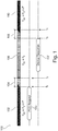
- FIG. 2 which in its lower part shows a more detailed overview 201 of the transmission phase 106/206 discussed above in conjunction with Figure 1 .
- the upper part 200 of Figure 2 corresponds to the illustration of Figure 1 .
- the detailed overview 201 shows a control signal 212 for controlling an adjustable resistive circuit.
- the shown control signal 212 has the shape of a square wave, but other embodiments may use other waveforms.
- the control signal is high, the resistance of the adjustable resistive circuit is increased such that the resistance of the antenna circuit is increased.
- the control signal 212 is low during the periods 216.
- FIG. 3 shows a circuit diagram of an RF device 320 in accordance with an embodiment. More specifically, the RF device 320 comprises a control unit 322 and a main resonance circuit 324 connected to antenna 326. Furthermore, the RF device 320 comprises switchable capacitors C 2B , which are connected to switches (not shown) within the control unit 322 via connecting wires 328 and 329. Yet further, the RF device 320 comprises an adjustable resistive circuit 330 comprising resistors R TX . The resistance of resistors R TX can be adjusted such that the Q-factor of the complete resonance circuit is adjusted accordingly.
- the control unit 322 connects the wires 328 and 329 to GND (ground) such that the capacitors C 2B are now connected in parallel with capacitors C 2A of the main resonance circuit 324.
- the resonance frequency of the complete resonance circuit is influenced by the capacitors C 2B .
- the Q-factor is also relatively large in comparison to the receiving mode.
- the control unit 322 further operates to periodically adjust the resistors R TX such that the Q-factor of the resonance circuit alternates between the aforementioned relatively large value and a somewhat lower value due to the alternating resistance of the circuit.
Landscapes
- Engineering & Computer Science (AREA)
- Computer Networks & Wireless Communication (AREA)
- Signal Processing (AREA)
- Near-Field Transmission Systems (AREA)
- Power Engineering (AREA)
Claims (9)
- Eine RF bidirektionale Kommunikationsvorrichtung, welche eine aktive Lastmodulation verwendet, wobei die Vorrichtung aufweisteinen Resonanz Schaltkreis, welcher eine Antenne (326), einen einstellbaren resistiven Schaltkreis (330), und eine Steuereinheit (322) zum Steuern der Kommunikation der Vorrichtung enthält, einschließlich eines Schaltens zwischen einem Sendemodus und einem Empfangsmodus,
wobei die Steuereinheit eingerichtet ist zumModifizieren einer Konfiguration des Resonanz Schaltkreises derartig, dass der Resonanz Schaltkreis eine erste Resonanzfrequenz (f0 + Δf, f0 - Δf) hat, wenn die Vorrichtung in dem Empfangsmodus ist, und eine zweite Resonanzfrequenz (f0) hat, wenn die Vorrichtung in dem Sendemodus ist,
dadurch gekennzeichnet, dass die Steuereinheit eingerichtet ist zumEinstellen des Widerstands des resistiven Schaltkreises in einer alternierende Weise, wenn die Vorrichtung in dem Sendemodus ist, derartig, dass ein Q-Faktor des Resonanz Schaltkreises periodisch modifiziert wird, während die Vorrichtung in dem Sendemodus ist, wobei der einstellbare resistive Schaltkreis (330) durch ein periodisches Steuersignal (212) gesteuert wird. - Die Vorrichtung gemäß dem vorangehenden Anspruch, wobeider Resonanz Schaltkreis einen schaltbaren kapazitiven Schaltkreis (328, 329) aufweist, unddie Steuereinheit eingerichtet ist zum Modifizieren der Konfiguration des Resonanz Schaltkreises mittels selektiven Verbindens und Trennens des schaltbaren kapazitiven Schaltkreises.
- Die Vorrichtung gemäß dem vorangehenden Anspruch, wobeidie Steuereinheit eingerichtet ist zum Verbinden des schaltbaren kapazitiven Schaltkreises beim Schalten von dem Empfangsmodus zu dem Sendemodus und zum Trennen des schaltbaren kapazitiven Schaltkreises beim Schalten von dem Sendemodus zu dem Empfangsmodus.
- Die Vorrichtung gemäß irgendeinem der vorangehenden Ansprüche, wobeidie erste Resonanzfrequenz 14,4075 MHz ist und/oder die zweite Resonanzfrequenz 13,56 MHz ist.
- Ein Verfahren zum Ausführen einer bidirektionalen Kommunikation zwischen einer RF Vorrichtung (320) und einer Leser/Schreiber Vorrichtung, wobei das Verfahren aufweistEinstellen der RF Vorrichtung, in einem Empfangsmodus zu arbeiten, mittels Konfigurierens eines Resonanz Schaltkreises der RF Vorrichtung, eine erste Resonanzfrequenz zu haben, wobei der Resonanzschaltkreis eine Antenne (326) und einen einstellbaren resistiven Schaltkreis (330) enthält,Empfangen, an der RF Vorrichtung, einer Anfrage zum Senden von der Leser/Schreiber Vorrichtung,Einstellen der RF Vorrichtung, in einem Sendemodus zu arbeiten, mittels Konfigurierens des Resonanz Schaltkreises der RF Vorrichtung, eine zweite Resonanzfrequenz zu haben,wobei das Verfahren dadurch gekennzeichnet ist, dass es aufweistwährend des Arbeitens in dem Sendemodus, Einstellen des Widerstands des resistiven Schaltkreises in einer alternierende Weise durch ein periodisches Steuersignal (212) derartig, dass ein Q-Faktor des Resonanz Schaltkreises der RF Vorrichtung periodisch modifiziert wird.
- Das Verfahren gemäß dem vorangehenden Anspruch, ferner aufweisendnach einem Beenden des Arbeitens in dem Sendemodus, Neu-Einstellen der RF Vorrichtung, in dem Empfangsmodus zu arbeiten, mittels Konfigurierens des Resonanz Schaltkreises der RF Vorrichtung, die erste Resonanzfrequenz zu haben.
- Ein Computerprogramm aufweisend Computer ausführbare Anweisungen, welche, wenn sie mittels eines Computers ausgeführt werden, den Computer veranlassen, die Schritte des Verfahrens gemäß Anspruch 5 oder 6 auszuführen.
- Ein Computerprogramm Produkt aufweisend einen Computer lesbaren Datenträger, auf welchem ein Computerprogramm gemäß Anspruch 7 geladen ist.
- Ein System zum Ausführen einer bidirektionalen RF Kommunikation, wobei das System aufweisteine Leser/Schreiber Vorrichtung, undeine Vorrichtung gemäß irgendeinem der Ansprüche 1 bis 4.
Priority Applications (3)
| Application Number | Priority Date | Filing Date | Title |
|---|---|---|---|
| EP13177543.9A EP2830228B1 (de) | 2013-07-23 | 2013-07-23 | HF-Vorrichtung und Verfahren mit verbesserter aktiver Belastungsmodulationskapazität |
| US14/321,433 US9401739B2 (en) | 2013-07-23 | 2014-07-01 | RF device and method with improved active load modulation capability |
| CN201410344732.2A CN104348515B (zh) | 2013-07-23 | 2014-07-18 | 具有改进的有源负载调制能力的rf装置和方法 |
Applications Claiming Priority (1)
| Application Number | Priority Date | Filing Date | Title |
|---|---|---|---|
| EP13177543.9A EP2830228B1 (de) | 2013-07-23 | 2013-07-23 | HF-Vorrichtung und Verfahren mit verbesserter aktiver Belastungsmodulationskapazität |
Publications (2)
| Publication Number | Publication Date |
|---|---|
| EP2830228A1 EP2830228A1 (de) | 2015-01-28 |
| EP2830228B1 true EP2830228B1 (de) | 2018-01-10 |
Family
ID=48877043
Family Applications (1)
| Application Number | Title | Priority Date | Filing Date |
|---|---|---|---|
| EP13177543.9A Active EP2830228B1 (de) | 2013-07-23 | 2013-07-23 | HF-Vorrichtung und Verfahren mit verbesserter aktiver Belastungsmodulationskapazität |
Country Status (3)
| Country | Link |
|---|---|
| US (1) | US9401739B2 (de) |
| EP (1) | EP2830228B1 (de) |
| CN (1) | CN104348515B (de) |
Families Citing this family (15)
| Publication number | Priority date | Publication date | Assignee | Title |
|---|---|---|---|---|
| FR3037201B1 (fr) * | 2015-06-02 | 2018-07-13 | Stmicroelectronics (Rousset) Sas | Procede de controle de l'accord sur une frequence de communication d'une antenne connectee a un composant adapte a une communication sans contact, et systeme correspondant |
| US10666325B2 (en) | 2016-04-01 | 2020-05-26 | Nan Jing Qiwei Technology Limited | Near-field communication (NFC) system and method for high performance NFC and wireless power transfer with small antennas |
| US10153809B2 (en) * | 2016-04-01 | 2018-12-11 | Fusens Technology Limited | Near-field communication (NFC) reader optimized for high performance NFC and wireless power transfer with small antennas |
| US10461812B2 (en) | 2016-04-01 | 2019-10-29 | Nan Jing Qiwei Technology Limited | Near-field communication (NFC) tags optimized for high performance NFC and wireless power reception with small antennas |
| US9806771B1 (en) * | 2016-08-01 | 2017-10-31 | Nxp B.V. | Method and system for high resolution tuning of the phase for active load modulation in a NFC system |
| US9911075B1 (en) | 2016-09-01 | 2018-03-06 | Nxp B.V. | RFID transponder and method for supplying energy thereto |
| US10110281B2 (en) | 2017-03-17 | 2018-10-23 | Nxp B.V. | Near field communication device |
| US10361474B2 (en) * | 2017-03-17 | 2019-07-23 | Nxp B.V. | Near field communication device |
| US10200091B2 (en) * | 2017-06-13 | 2019-02-05 | Nxp B.V. | RF front end module and near field communication device |
| FR3070563A1 (fr) * | 2017-08-31 | 2019-03-01 | Stmicroelectronics (Rousset) Sas | Circuit de pilotage d'antenne nfc |
| FR3074379B1 (fr) * | 2017-11-24 | 2020-11-13 | Continental Automotive France | Lecteur d'authentification pour ouvrant de vehicule automobile |
| US10516445B2 (en) | 2018-04-11 | 2019-12-24 | Nxp B.V. | RF front end module and near field communication device |
| US11038553B2 (en) | 2018-12-10 | 2021-06-15 | Nxp B.V. | EMC inductor-free RF front-end method and topology with power by field function for an inductively coupled communication system |
| CN111769655B (zh) | 2020-05-19 | 2022-09-23 | 华为技术有限公司 | 一种终端设备及其控制方法 |
| CN117121303A (zh) * | 2022-03-23 | 2023-11-24 | 京东方科技集团股份有限公司 | 天线阻抗匹配的设计电路及近场通信电路系统 |
Family Cites Families (9)
| Publication number | Priority date | Publication date | Assignee | Title |
|---|---|---|---|---|
| DE10119489C1 (de) * | 2001-04-20 | 2002-07-25 | Texas Instruments Deutschland | Batterieloser Transponder |
| US7936272B2 (en) * | 2006-06-29 | 2011-05-03 | Allflex Usa, Inc. | Dynamic antenna tuning circuit for a radio frequency identification reader |
| JP4787945B2 (ja) * | 2006-07-14 | 2011-10-05 | ソニー・エリクソン・モバイルコミュニケーションズ株式会社 | 非接触通信回路及び携帯端末 |
| GB0705635D0 (en) * | 2007-03-23 | 2007-05-02 | Innovision Res & Tech Plc | Near field RF communicators |
| US8369786B2 (en) * | 2008-05-05 | 2013-02-05 | Nxp B.V. | Radio frequency communication device and method for operating the same |
| EP2302567B1 (de) | 2009-09-17 | 2015-11-11 | Nxp B.V. | Oberflächentolerante RFID-Transpondervorrichtung |
| NO2486552T3 (de) * | 2009-10-09 | 2018-01-27 | ||
| SK288555B6 (sk) * | 2009-11-14 | 2018-05-02 | Smk Corporation | Spôsob a systém na prenos dát z transpondera do čítačky, najmä pri platobných aplikáciách s mobilným komunikačným zariadením |
| US9331378B2 (en) | 2012-05-29 | 2016-05-03 | Nxp B.V. | Active load modulation antenna |
-
2013
- 2013-07-23 EP EP13177543.9A patent/EP2830228B1/de active Active
-
2014
- 2014-07-01 US US14/321,433 patent/US9401739B2/en active Active
- 2014-07-18 CN CN201410344732.2A patent/CN104348515B/zh active Active
Non-Patent Citations (1)
| Title |
|---|
| None * |
Also Published As
| Publication number | Publication date |
|---|---|
| US9401739B2 (en) | 2016-07-26 |
| US20150031315A1 (en) | 2015-01-29 |
| CN104348515A (zh) | 2015-02-11 |
| EP2830228A1 (de) | 2015-01-28 |
| CN104348515B (zh) | 2017-04-12 |
Similar Documents
| Publication | Publication Date | Title |
|---|---|---|
| EP2830228B1 (de) | HF-Vorrichtung und Verfahren mit verbesserter aktiver Belastungsmodulationskapazität | |
| US10997483B2 (en) | NFC antenna switch | |
| KR101707480B1 (ko) | 근접 장 통신 디바이스들에서의 직접 전력 송신 로드 변조 | |
| EP2266076B1 (de) | Sende-/empfangsschaltung für kontaktlose kommunikation und nfc vorrichtung oder rfid lese-/schreibvorrichtung mit entsprechende sende-/empfangsschaltung | |
| KR102022867B1 (ko) | Nfc 회로 및 이의 동작 방법 | |
| US9729202B2 (en) | Method of connecting one or more contactless components to a single antenna, and corresponding system | |
| US10686495B2 (en) | Frequency adjustment of an NFC circuit | |
| CN108649989B (zh) | 具有远程天线的nfc读取器 | |
| US20140148097A1 (en) | System for near field communication (nfc) and frequency modulation (fm) communication and portable electronic device using the same | |
| US10419058B2 (en) | Method for controlling the tuning to a communications frequency of an antenna connected to a component designed for contactless communication and corresponding system | |
| US20180109294A1 (en) | Method for managing contactless communications and contractless charging with a system, and corresponding system | |
| US20130203355A1 (en) | Short-distance wireless communication device | |
| WO2014037393A1 (en) | Method and circuit for tuning an antenna circuit of an actively transmitting tag | |
| JP5803550B2 (ja) | アンテナ回路、通信装置、および通信方法 | |
| KR20140018603A (ko) | Rfid 리더기, rfid 태그 및 rfid 시스템 | |
| US20220407566A1 (en) | Impedance matching in near-field rf communication devices | |
| US9401542B2 (en) | Antenna arrangement | |
| CN118842487A (zh) | 近场通信电路 | |
| CN115412130A (zh) | Rfid标签自调谐 | |
| KR20120103298A (ko) | Nfc 안테나 모듈 | |
| US9516454B2 (en) | Near-field communication system terminal | |
| HK1177819A1 (zh) | 控制近场通信装置的天线特性 |
Legal Events
| Date | Code | Title | Description |
|---|---|---|---|
| 17P | Request for examination filed |
Effective date: 20140326 |
|
| AK | Designated contracting states |
Kind code of ref document: A1 Designated state(s): AL AT BE BG CH CY CZ DE DK EE ES FI FR GB GR HR HU IE IS IT LI LT LU LV MC MK MT NL NO PL PT RO RS SE SI SK SM TR |
|
| AX | Request for extension of the european patent |
Extension state: BA ME |
|
| PUAI | Public reference made under article 153(3) epc to a published international application that has entered the european phase |
Free format text: ORIGINAL CODE: 0009012 |
|
| RBV | Designated contracting states (corrected) |
Designated state(s): AL AT BE BG CH CY CZ DE DK EE ES FI FR GB GR HR HU IE IS IT LI LT LU LV MC MK MT NL NO PL PT RO RS SE SI SK SM TR |
|
| 17Q | First examination report despatched |
Effective date: 20161129 |
|
| GRAP | Despatch of communication of intention to grant a patent |
Free format text: ORIGINAL CODE: EPIDOSNIGR1 |
|
| INTG | Intention to grant announced |
Effective date: 20170829 |
|
| GRAS | Grant fee paid |
Free format text: ORIGINAL CODE: EPIDOSNIGR3 |
|
| GRAA | (expected) grant |
Free format text: ORIGINAL CODE: 0009210 |
|
| AK | Designated contracting states |
Kind code of ref document: B1 Designated state(s): AL AT BE BG CH CY CZ DE DK EE ES FI FR GB GR HR HU IE IS IT LI LT LU LV MC MK MT NL NO PL PT RO RS SE SI SK SM TR |
|
| REG | Reference to a national code |
Ref country code: CH Ref legal event code: EP Ref country code: AT Ref legal event code: REF Ref document number: 963503 Country of ref document: AT Kind code of ref document: T Effective date: 20180115 |
|
| REG | Reference to a national code |
Ref country code: IE Ref legal event code: FG4D |
|
| REG | Reference to a national code |
Ref country code: DE Ref legal event code: R096 Ref document number: 602013031878 Country of ref document: DE |
|
| REG | Reference to a national code |
Ref country code: NL Ref legal event code: MP Effective date: 20180110 |
|
| REG | Reference to a national code |
Ref country code: AT Ref legal event code: MK05 Ref document number: 963503 Country of ref document: AT Kind code of ref document: T Effective date: 20180110 |
|
| REG | Reference to a national code |
Ref country code: FR Ref legal event code: PLFP Year of fee payment: 6 |
|
| PG25 | Lapsed in a contracting state [announced via postgrant information from national office to epo] |
Ref country code: NL Free format text: LAPSE BECAUSE OF FAILURE TO SUBMIT A TRANSLATION OF THE DESCRIPTION OR TO PAY THE FEE WITHIN THE PRESCRIBED TIME-LIMIT Effective date: 20180110 |
|
| PG25 | Lapsed in a contracting state [announced via postgrant information from national office to epo] |
Ref country code: FI Free format text: LAPSE BECAUSE OF FAILURE TO SUBMIT A TRANSLATION OF THE DESCRIPTION OR TO PAY THE FEE WITHIN THE PRESCRIBED TIME-LIMIT Effective date: 20180110 Ref country code: NO Free format text: LAPSE BECAUSE OF FAILURE TO SUBMIT A TRANSLATION OF THE DESCRIPTION OR TO PAY THE FEE WITHIN THE PRESCRIBED TIME-LIMIT Effective date: 20180410 Ref country code: CY Free format text: LAPSE BECAUSE OF FAILURE TO SUBMIT A TRANSLATION OF THE DESCRIPTION OR TO PAY THE FEE WITHIN THE PRESCRIBED TIME-LIMIT Effective date: 20180110 Ref country code: LT Free format text: LAPSE BECAUSE OF FAILURE TO SUBMIT A TRANSLATION OF THE DESCRIPTION OR TO PAY THE FEE WITHIN THE PRESCRIBED TIME-LIMIT Effective date: 20180110 Ref country code: ES Free format text: LAPSE BECAUSE OF FAILURE TO SUBMIT A TRANSLATION OF THE DESCRIPTION OR TO PAY THE FEE WITHIN THE PRESCRIBED TIME-LIMIT Effective date: 20180110 Ref country code: HR Free format text: LAPSE BECAUSE OF FAILURE TO SUBMIT A TRANSLATION OF THE DESCRIPTION OR TO PAY THE FEE WITHIN THE PRESCRIBED TIME-LIMIT Effective date: 20180110 |
|
| PG25 | Lapsed in a contracting state [announced via postgrant information from national office to epo] |
Ref country code: GR Free format text: LAPSE BECAUSE OF FAILURE TO SUBMIT A TRANSLATION OF THE DESCRIPTION OR TO PAY THE FEE WITHIN THE PRESCRIBED TIME-LIMIT Effective date: 20180411 Ref country code: BG Free format text: LAPSE BECAUSE OF FAILURE TO SUBMIT A TRANSLATION OF THE DESCRIPTION OR TO PAY THE FEE WITHIN THE PRESCRIBED TIME-LIMIT Effective date: 20180410 Ref country code: PL Free format text: LAPSE BECAUSE OF FAILURE TO SUBMIT A TRANSLATION OF THE DESCRIPTION OR TO PAY THE FEE WITHIN THE PRESCRIBED TIME-LIMIT Effective date: 20180110 Ref country code: AT Free format text: LAPSE BECAUSE OF FAILURE TO SUBMIT A TRANSLATION OF THE DESCRIPTION OR TO PAY THE FEE WITHIN THE PRESCRIBED TIME-LIMIT Effective date: 20180110 Ref country code: IS Free format text: LAPSE BECAUSE OF FAILURE TO SUBMIT A TRANSLATION OF THE DESCRIPTION OR TO PAY THE FEE WITHIN THE PRESCRIBED TIME-LIMIT Effective date: 20180510 Ref country code: LV Free format text: LAPSE BECAUSE OF FAILURE TO SUBMIT A TRANSLATION OF THE DESCRIPTION OR TO PAY THE FEE WITHIN THE PRESCRIBED TIME-LIMIT Effective date: 20180110 Ref country code: RS Free format text: LAPSE BECAUSE OF FAILURE TO SUBMIT A TRANSLATION OF THE DESCRIPTION OR TO PAY THE FEE WITHIN THE PRESCRIBED TIME-LIMIT Effective date: 20180110 Ref country code: SE Free format text: LAPSE BECAUSE OF FAILURE TO SUBMIT A TRANSLATION OF THE DESCRIPTION OR TO PAY THE FEE WITHIN THE PRESCRIBED TIME-LIMIT Effective date: 20180110 |
|
| REG | Reference to a national code |
Ref country code: DE Ref legal event code: R097 Ref document number: 602013031878 Country of ref document: DE |
|
| PG25 | Lapsed in a contracting state [announced via postgrant information from national office to epo] |
Ref country code: AL Free format text: LAPSE BECAUSE OF FAILURE TO SUBMIT A TRANSLATION OF THE DESCRIPTION OR TO PAY THE FEE WITHIN THE PRESCRIBED TIME-LIMIT Effective date: 20180110 Ref country code: RO Free format text: LAPSE BECAUSE OF FAILURE TO SUBMIT A TRANSLATION OF THE DESCRIPTION OR TO PAY THE FEE WITHIN THE PRESCRIBED TIME-LIMIT Effective date: 20180110 Ref country code: EE Free format text: LAPSE BECAUSE OF FAILURE TO SUBMIT A TRANSLATION OF THE DESCRIPTION OR TO PAY THE FEE WITHIN THE PRESCRIBED TIME-LIMIT Effective date: 20180110 Ref country code: IT Free format text: LAPSE BECAUSE OF FAILURE TO SUBMIT A TRANSLATION OF THE DESCRIPTION OR TO PAY THE FEE WITHIN THE PRESCRIBED TIME-LIMIT Effective date: 20180110 |
|
| PLBE | No opposition filed within time limit |
Free format text: ORIGINAL CODE: 0009261 |
|
| STAA | Information on the status of an ep patent application or granted ep patent |
Free format text: STATUS: NO OPPOSITION FILED WITHIN TIME LIMIT |
|
| PG25 | Lapsed in a contracting state [announced via postgrant information from national office to epo] |
Ref country code: CZ Free format text: LAPSE BECAUSE OF FAILURE TO SUBMIT A TRANSLATION OF THE DESCRIPTION OR TO PAY THE FEE WITHIN THE PRESCRIBED TIME-LIMIT Effective date: 20180110 Ref country code: SM Free format text: LAPSE BECAUSE OF FAILURE TO SUBMIT A TRANSLATION OF THE DESCRIPTION OR TO PAY THE FEE WITHIN THE PRESCRIBED TIME-LIMIT Effective date: 20180110 Ref country code: DK Free format text: LAPSE BECAUSE OF FAILURE TO SUBMIT A TRANSLATION OF THE DESCRIPTION OR TO PAY THE FEE WITHIN THE PRESCRIBED TIME-LIMIT Effective date: 20180110 Ref country code: SK Free format text: LAPSE BECAUSE OF FAILURE TO SUBMIT A TRANSLATION OF THE DESCRIPTION OR TO PAY THE FEE WITHIN THE PRESCRIBED TIME-LIMIT Effective date: 20180110 |
|
| 26N | No opposition filed |
Effective date: 20181011 |
|
| PG25 | Lapsed in a contracting state [announced via postgrant information from national office to epo] |
Ref country code: SI Free format text: LAPSE BECAUSE OF FAILURE TO SUBMIT A TRANSLATION OF THE DESCRIPTION OR TO PAY THE FEE WITHIN THE PRESCRIBED TIME-LIMIT Effective date: 20180110 |
|
| REG | Reference to a national code |
Ref country code: CH Ref legal event code: PL |
|
| GBPC | Gb: european patent ceased through non-payment of renewal fee |
Effective date: 20180723 |
|
| PG25 | Lapsed in a contracting state [announced via postgrant information from national office to epo] |
Ref country code: LU Free format text: LAPSE BECAUSE OF NON-PAYMENT OF DUE FEES Effective date: 20180723 Ref country code: MC Free format text: LAPSE BECAUSE OF FAILURE TO SUBMIT A TRANSLATION OF THE DESCRIPTION OR TO PAY THE FEE WITHIN THE PRESCRIBED TIME-LIMIT Effective date: 20180110 |
|
| REG | Reference to a national code |
Ref country code: BE Ref legal event code: MM Effective date: 20180731 |
|
| REG | Reference to a national code |
Ref country code: IE Ref legal event code: MM4A |
|
| PG25 | Lapsed in a contracting state [announced via postgrant information from national office to epo] |
Ref country code: GB Free format text: LAPSE BECAUSE OF NON-PAYMENT OF DUE FEES Effective date: 20180723 Ref country code: CH Free format text: LAPSE BECAUSE OF NON-PAYMENT OF DUE FEES Effective date: 20180731 Ref country code: IE Free format text: LAPSE BECAUSE OF NON-PAYMENT OF DUE FEES Effective date: 20180723 Ref country code: LI Free format text: LAPSE BECAUSE OF NON-PAYMENT OF DUE FEES Effective date: 20180731 |
|
| PG25 | Lapsed in a contracting state [announced via postgrant information from national office to epo] |
Ref country code: BE Free format text: LAPSE BECAUSE OF NON-PAYMENT OF DUE FEES Effective date: 20180731 |
|
| PG25 | Lapsed in a contracting state [announced via postgrant information from national office to epo] |
Ref country code: MT Free format text: LAPSE BECAUSE OF NON-PAYMENT OF DUE FEES Effective date: 20180723 |
|
| PG25 | Lapsed in a contracting state [announced via postgrant information from national office to epo] |
Ref country code: TR Free format text: LAPSE BECAUSE OF FAILURE TO SUBMIT A TRANSLATION OF THE DESCRIPTION OR TO PAY THE FEE WITHIN THE PRESCRIBED TIME-LIMIT Effective date: 20180110 |
|
| PG25 | Lapsed in a contracting state [announced via postgrant information from national office to epo] |
Ref country code: HU Free format text: LAPSE BECAUSE OF FAILURE TO SUBMIT A TRANSLATION OF THE DESCRIPTION OR TO PAY THE FEE WITHIN THE PRESCRIBED TIME-LIMIT; INVALID AB INITIO Effective date: 20130723 Ref country code: PT Free format text: LAPSE BECAUSE OF FAILURE TO SUBMIT A TRANSLATION OF THE DESCRIPTION OR TO PAY THE FEE WITHIN THE PRESCRIBED TIME-LIMIT Effective date: 20180110 |
|
| PG25 | Lapsed in a contracting state [announced via postgrant information from national office to epo] |
Ref country code: MK Free format text: LAPSE BECAUSE OF NON-PAYMENT OF DUE FEES Effective date: 20180110 |
|
| P01 | Opt-out of the competence of the unified patent court (upc) registered |
Effective date: 20230725 |
|
| PGFP | Annual fee paid to national office [announced via postgrant information from national office to epo] |
Ref country code: FR Payment date: 20250620 Year of fee payment: 13 |
|
| PGFP | Annual fee paid to national office [announced via postgrant information from national office to epo] |
Ref country code: DE Payment date: 20250620 Year of fee payment: 13 |