EP2830273B1 - Dispositif et procédé de correction de communications - Google Patents
Dispositif et procédé de correction de communications Download PDFInfo
- Publication number
- EP2830273B1 EP2830273B1 EP12741531.3A EP12741531A EP2830273B1 EP 2830273 B1 EP2830273 B1 EP 2830273B1 EP 12741531 A EP12741531 A EP 12741531A EP 2830273 B1 EP2830273 B1 EP 2830273B1
- Authority
- EP
- European Patent Office
- Prior art keywords
- analogue
- digital
- channel
- signal
- correction
- Prior art date
- Legal status (The legal status is an assumption and is not a legal conclusion. Google has not performed a legal analysis and makes no representation as to the accuracy of the status listed.)
- Active
Links
Images




Classifications
-
- H—ELECTRICITY
- H04—ELECTRIC COMMUNICATION TECHNIQUE
- H04B—TRANSMISSION
- H04B1/00—Details of transmission systems, not covered by a single one of groups H04B3/00 - H04B13/00; Details of transmission systems not characterised by the medium used for transmission
- H04B1/06—Receivers
- H04B1/10—Means associated with receiver for limiting or suppressing noise or interference
-
- H—ELECTRICITY
- H04—ELECTRIC COMMUNICATION TECHNIQUE
- H04L—TRANSMISSION OF DIGITAL INFORMATION, e.g. TELEGRAPHIC COMMUNICATION
- H04L1/00—Arrangements for detecting or preventing errors in the information received
- H04L1/22—Arrangements for detecting or preventing errors in the information received using redundant apparatus to increase reliability
-
- H—ELECTRICITY
- H04—ELECTRIC COMMUNICATION TECHNIQUE
- H04B—TRANSMISSION
- H04B1/00—Details of transmission systems, not covered by a single one of groups H04B3/00 - H04B13/00; Details of transmission systems not characterised by the medium used for transmission
- H04B1/06—Receivers
- H04B1/10—Means associated with receiver for limiting or suppressing noise or interference
- H04B1/12—Neutralising, balancing, or compensation arrangements
- H04B1/123—Neutralising, balancing, or compensation arrangements using adaptive balancing or compensation means
-
- H—ELECTRICITY
- H04—ELECTRIC COMMUNICATION TECHNIQUE
- H04B—TRANSMISSION
- H04B17/00—Monitoring; Testing
- H04B17/20—Monitoring; Testing of receivers
- H04B17/21—Monitoring; Testing of receivers for calibration; for correcting measurements
- H04B17/22—Monitoring; Testing of receivers for calibration; for correcting measurements for calibration of the receiver components
Definitions
- the present invention relates to radio communications technologies, and in particular, to a device and method for communication correction.
- FIG. 1 is a structural block diagram of a receiver in an existing radio communications system.
- the receiver mainly includes an analogue radio-frequency front end 101, an analogue demodulator and intermediate-frequency channel 102, and an analogue-to-digital converter (Analogue to Digital Converter, ADC) 103.
- the analogue radio-frequency front end 101 generally includes a low noise amplifier (Low Noise Amplifier, LNA).
- LNA Low Noise Amplifier
- various receivers in the radio communications system all have the non-ideal characteristics.
- an analogue IQ demodulation receiver the non-ideal characteristics thereof are reflected in unbalanced amplitudes and phases of in-phase and quadrature (Inphase and Quadrature, IQ) signals, direct current (Direct Current, DC) interference, an in-band amplitude ripple and a group delay ripple in a radio-frequency filter of an analogue radio-frequency front end, non-linear distortion, and so on.
- in-phase and Quadrature, IQ in-phase and Quadrature
- DC Direct Current
- the non-ideal characteristics thereof are reflected in an in-band amplitude ripple and a group delay ripple in a radio-frequency filter, an in-band amplitude ripple and a group delay ripple imported by an intermediate-frequency surface acoustic wave (SAW) filter, non-linear distortion, and so on.
- SAW surface acoustic wave
- a correction channel is often used to correct the non-ideal characteristics of a receiver.
- a test signal producing device is used to produce a radio-frequency test signal in a certain form, and at an input end of a receiver, the radio-frequency test signal and an input radio-frequency analogue signal are mixed by using a coupler or a resistor network and are sent to the input end of the receiver together.
- the test signal producing device further sends a signal of a digital form corresponding to the radio-frequency test signal to a channel correction module to be corrected by the channel correction module. After the correction performed by the channel correction module, cancellation processing is performed on the test signal, so as to attempt to eliminate the interference of the test signal to a service signal.
- the cancellation processing performed on the test signal is not completely ideal, and a signal output after the cancellation processing still has certain residues of the test signal, which causes the interference to the service signal.
- the receiver includes a first receiver path configured to receive an input signal.
- the first receiver path outputs a signal including at least one baseband (BB) frequency.
- At least one second receiver path is configured to receive the input signal and to provide a second receiver path output signal.
- the second receiver path includes at least one odd-order nonlinear distortion reference generator.
- the at least one odd-order nonlinear distortion reference generator and the mixer are configured to generate a synthetic odd-order nonlinear distortion signal.
- a combining element is configured to receive the output signal from the first path and the output signal from the second receiver path output and to combine the signals such that the odd-order nonlinear distortion signals are substantially attenuated at an output of the combining element.
- Document WO 2003/065602 A2 discloses techniques for compensating for second-order distortion in a wireless communication device.
- IM2 distortion generated by the mixer (20) results in undesirable distortion levels in the baseband output signal.
- a compensation circuit (104) provides a measure of the IM2 distortion current independent of the radio frequency (RF) pathway to generate an IM2 calibration current.
- the IM2 calibration current is combined with the baseband output signal to thereby eliminate the IM2 currents generated within the RF pathway.
- the calibration is provided at the factory during final testing.
- additional circuitry (156, 158) may be added to the wireless communication device to provide a pathway between the transmitter (150) and the receiver (146).
- the transmitter signal is provided to the receiver to permit automatic calibration of the unit.
- An internal signal source (162) may be used in place of the transmitter (150).
- the auto-calibration may be performed to eliminate IM2 distortion or permit optimization of the circuit to minimize other forms of distortion or interference.
- the present invention provides a device and method for communication correction, which are used to solve a problem of causing interference to a service signal when a test signal is used to correct a channel of a receiver in the prior art.
- the present invention provides a device for communication correction, which includes a receiving channel and a correction channel, where the receiving channel includes an analogue radio-frequency front end, a demodulator, a first analogue-to-digital converter, and a first channel correction module; and the correction channel includes a frequency converter, a second analogue-to-digital converter, and a digital processor, where the analogue radio-frequency front end is connected to both the demodulator and the frequency converter, and is configured to amplify a received radio-frequency analogue signal, and output the amplified analogue signal to both the demodulator and the frequency converter; the demodulator is connected to the first analogue-to-digital converter, and is configured to demodulated the amplified analogue signal, and output the demodulated analogue signal to the first analogue-to-digital converter; the first analogue-to-digital converter is further connected to the first channel correction module, and is configured to perform analogue-to-digital conversion on
- the present invention provides a method for communication correction, which includes:
- a received service signal is divided, and the service signal itself is used to correct a channel of the receiver, so as to not only correct the non-ideal characteristics of the receiver through the correction channel, but also solve the problem of causing the interference to the service signal because of incomplete cancellation of the test signal when the test signal is used to correct the channel of the receiver in the prior art.
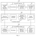
- FIG. 2 is a schematic structural diagram of a device for communication correction according to an embodiment of the present invention. As shown in FIG. 2 , the device in this embodiment includes a receiving channel 100 and a correction channel 200.
- the receiving channel 100 mainly includes an analogue radio-frequency front end 11, a demodulator 12, a first analogue-to-digital converter 13, and a first channel correction module 14.
- the analogue radio-frequency front end 11 is connected to the demodulator 12; the demodulator 12 is connected to the first analogue-to-digital converter 13; and the first analogue-to-digital converter 13 is connected to the first channel correction module 14.
- the correction channel 200 mainly includes a frequency converter 21, a second analogue-to-digital converter 22, and a digital processor 23.
- the frequency converter 21 is connected to the second analogue-to-digital converter 22; and the second analogue-to-digital converter 22 is connected to the digital processor 23.
- the analogue radio-frequency front end 11 is further connected to the frequency converter 21; and the digital processor 23 is further connected to the first channel correction module 14.
- the structure of the receiving channel 100 in this embodiment is similar to a structure of a receiver in an existing communications system, and the difference lies in that functions of some components are not exactly the same.
- a function of each component in the receiving channel 100 is as follows:
- the analogue radio-frequency front end 11 is mainly configured to receive a radio-frequency analogue signal, amplify the radio-frequency analogue signal, and then output the amplified analogue signal to both the demodulator 12 and the frequency converter 21.
- the amplifying mainly refers to low noise amplifying. That is to say, the analogue radio-frequency front end 11 in this embodiment outputs two paths of analogue signals after performing low noise amplifying on the received radio-frequency analogue signal. One of the two paths of analogue signals is input to the demodulator 12 that is connected to the analogue radio-frequency front end 11, and the other path is input to the frequency converter 21 that is connected to the analogue radio-frequency front end 11.
- the analogue radio-frequency front end 11 in this embodiment is mainly composed of some LNAs and a filter.
- the demodulator 12 is configured to receive an analogue signal, demodulate the received analogue signal, and then output the demodulated analogue signal to the first analogue-to-digital converter 13 connected to the demodulator 12.
- the analogue signal received by the demodulator 12 refers to one path of an analogue signal output by the analogue radio-frequency front end 11.
- the demodulator 12 in this embodiment may be composed of an analogue demodulator and an intermediate-frequency channel, which is not limited herein.
- the first analogue-to-digital converter 13 is configured to perform analogue-to-digital conversion on the received demodulated analogue signal to obtain a first digital signal, and then output the first digital signal to the first channel correction module 14, so that the first channel correction module 14 corrects the first digital signal, thereby achieving the objective of overcoming the non-ideal characteristics of the receiver.
- the first channel correction module 14 is configured to receive the first digital signal output by the first analogue-to-digital converter 13.
- a function of each component in the correction channel 200 in this embodiment is as follows:
- the frequency converter 21 is configured to receive an analogue signal, perform frequency conversion processing on the received analogue signal to obtain a first frequency conversion analogue signal, and then output the obtained first frequency conversion analogue signal to the second analogue-to-digital converter 22 connected to the frequency converter 21.
- the frequency converter 21 mainly converts a high-frequency signal (for example, 2100 MHz) into an intermediate-frequency signal (for example, 140 MHz).
- the analogue signal received by the frequency converter 21 is one path of an analogue signal output by the analogue radio-frequency front end 11.
- the frequency converter 21 in this embodiment may be composed of an analogue frequency converter and an intermediate-frequency channel, which is not limited herein.
- the second analogue-to-digital converter 22 is configured to receive the first frequency conversion analogue signal output by the frequency converter 21, perform analogue-to-digital conversion on the first frequency conversion analogue signal, convert the first frequency conversion analogue signal into a digital signal to obtain a digital signal after first analogue-to-digital conversion, and then output the digital signal after first analogue-to-digital conversion to the digital processor 23.
- the digital processor 23 is configured to receive the digital signal after first analogue-to-digital conversion, which is output by the second analogue-to-digital converter 22, perform digital processing on the digital signal after first analogue-to-digital conversion to obtain a second digital signal, and then output the second digital signal.
- the digital processor 23 outputs the second digital signal to the first channel correction module 14.
- the digital processor 23 may adopt a least square (Least Square, LS) algorithm and on the like to process the digital signal.
- the digital signal processed by the correction channel 200 is a real signal. Because the digital signal does not pass through the demodulator, the non-ideal characteristics of the demodulator and the complex signal (including IQ non-ideal characteristics) of the demodulator do not exist. Therefore, the digital signal can be used to compensate the non-ideal characteristics of the demodulator.
- the first channel correction module 14 not only receives the first digital signal output by the first analogue-to-digital converter 13, but also receives the second digital signal output by the digital processor 23, and corrects, according to the second digital signal output by the digital processor 23, the first digital signal output by the first analogue-to-digital converter 13, and outputs the corrected digital signal.
- the first digital signal output by the first analogue-to-digital converter 13 includes a direct current offset (DC-OFFSET) signal and a mirror image signal of the demodulator 12.
- the correction channel 200 does not demodulate the analogue signal, but the frequency converter 21 performs frequency conversion processing on the analogue signal. Therefore, the second digital signal output by the digital processor 23 does not include the DC-OFFSET signal and the mirror image signal.
- the first channel correction module 14 may adopt the LS algorithm and on the like to perform correlation comparison between one path of a digital signal from the first analogue-to-digital converter 13 and one path of a digital signal from the digital processor 23 to find the non-ideal characteristics, and then correct the found non-ideal characteristics.
- a channel of a receiver is corrected through the correction channel, so as to overcome various non-ideal characteristics of the receiver and improve the precision of the received digital signal.
- a service signal itself which is received by the receiver, is used to correct the channel of the receiver, and an external test signal is no longer used, so as to avoid a cancellation operation performed on the external test signal and solve a problem of causing interference to the service signal because of incomplete cancellation of the external test signal.
- FIG. 3 is a schematic structural diagram of a device for communication correction according to another embodiment of the present invention. This embodiment is implemented based on the embodiment shown in FIG. 2 . As shown in FIG. 3 , the device in this embodiment further includes a transmitting channel 300.
- the transmitting channel 300 mainly includes a second channel correction module 31, a digital-to-analogue converter 32, a modulator 33, and an analogue transmitting front end 34.
- the second channel correction module 31 is connected to the digital-to-analogue converter 32; the digital-to-analogue converter 32 is connected to the modulator 33; and the modulator 33 is connected to the analogue transmitting front end 34.
- correction channel 200 in this embodiment further includes a selection control module 24.
- the selection control module 24 is connected to a frequency converter 21.
- the analogue radio-frequency front end 11 is connected to the frequency converter 21 through the selection control module 24, that is to say, the selection control module 24 is connected between the analogue radio-frequency front end 11 and the frequency converter 21.
- the analogue transmitting front end 34 is connected to the frequency converter 21 through the selection control module 24, that is to say, the selection control module 24 is connected between the analogue transmitting front end 34 and the frequency converter 21.
- the digital processor 23 is further connected to the second channel correction module 31, and is further configured to provide a digital signal after digital processing to the second channel correction module 31.
- the selection control module 24 is configured to control the communication between the frequency converter 21 and the analogue radio-frequency front end 11, or control the communication between the frequency converter 21 and the analogue transmitting front end 34. That is to say, the correction channel 200 in this embodiment is connected to the receiving channel 100 and the transmitting channel 300 at the same time, and at a certain time, the correction channel 200 is in communication with one of the receiving channel 100 and the transmitting channel 300 through the selection control module 24, so that the correction channel 200 performs channel correction on the channel that is in communication with the correction channel 200.
- the frequency converter 21 in this embodiment is further configured to receive an analogue signal after power amplification, which is output by the analogue transmitting front end 34, perform frequency conversion processing on the analogue signal after power amplification to obtain a second frequency conversion analogue signal, and output the second frequency conversion analogue signal to the second analogue-to-digital converter 22.
- the second analogue-to-digital converter 22 is further configured to receive the second frequency conversion analogue signal output by the frequency converter 21, perform analogue-to-digital conversion on the second frequency conversion analogue signal output by the frequency converter 21 to obtain a digital signal after second analogue-to-digital conversion, and output the digital signal after second analogue-to-digital conversion to the digital processor 23.
- the digital processor 23 is further configured to receive the digital signal after second analogue-to-digital conversion, which is output by the second analogue-to-digital converter 22, perform digital processing on the digital signal after second analogue-to-digital conversion to obtain a third digital signal, and output the third digital signal to the second channel correction module 31, so that by using the third digital signal provided by the digital processor 23, the second channel correction module 31 corrects a fourth digital signal to be corrected, and outputs the corrected digital signal to the digital-to-analogue converter 32.
- the structure of the transmitting channel 300 in this embodiment is similar to a structure of a transmitter in an existing communications system, and the difference lies in that functions of some components are not exactly the same.
- a function of each component in the transmitting channel 300 is as follows:
- the second channel correction module 31, located in a receiving front end of the transmitting channel 300, is configured to receive the fourth digital signal to be corrected, receive the third digital signal that is output by the digital processor 23 and is obtained after digital processing, correct the fourth digital signal, which is to be corrected, by using the third digital signal provided by the digital processor 23, and output the corrected digital signal to the digital-to-analogue converter 32.
- the fourth digital signal to be corrected refers to a digital signal that needs to be transmitted by the transmitting channel 300.
- the fourth digital signal to be corrected may be a digital signal input from the outside.
- the second channel correction module 31 adopts an LS algorithm and on the like to perform correlation comparison between one path of a digital signal from the digital processor 23 and one path of an input digital signal to find non-ideal characteristics, and then correct the found non-ideal characteristics.
- the digital-to-analogue converter 32 is configured to receive the corrected digital signal output by the second channel correction module 31, perform digital-to-analogue conversion on the corrected digital signal, convert the received corrected digital signal into an analogue signal, and then output the analogue signal obtained through the digital-to-analogue conversion to the modulator 33.
- the modulator 33 is configured to receive the analogue signal output by the digital-to-analogue converter 32, modulate the received analogue signal, and output the modulated analogue signal to the analogue transmitting front end 34.
- the modulator 33 mainly modulates an intermediate-frequency signal onto a radio frequency, for example, adjusts a signal from 10 MHz to 2100 MHz, that is, shifts frequency spectrum.
- the modulator 33 in this embodiment may be composed of an analogue modulator and an intermediate-frequency channel, which is not limited herein.
- the analogue transmitting front end 34 is configured to receive the modulated analogue signal output by the modulator 33, perform power amplification processing on the received modulated analogue signal, transmit the analogue signal after power amplification, and output the analogue signal after power amplification to the frequency converter 21.
- the analogue transmitting front end 34 in this embodiment is generally composed of a power amplifier.
- the second channel correction module 31 specifically uses the characteristics of the transmitting channel 300, which are obtained by a previous digital signal, to correct a current digital signal, thereby overcoming various non-ideal characteristics of the transmitting channel 300, and improving the precision of transmitting the current digital signal.
- the foregoing previous digital signal is processed by the correction channel 200 to obtain the third digital signal, and the foregoing current digital signal is the fourth digital signal.
- a receiver has non-ideal characteristics
- a transmitter has non-ideal characteristics.
- the non-ideal characteristics of an analogue IQ modulation (also referred to as analogue quadrature modulation) transmitter are mainly reflected in a mirror image signal of an IQ signal and local oscillator feedthrough, which can seriously affect the precision of transmitting a signal.
- the device for communication correction in this embodiment is connected to the transmitting channel through the correction channel, and performs channel correction on the transmitting channel, thereby overcoming the non-ideal characteristics that exist in the transmitting channel, and improving the precision of transmitting a radio signal.
- the transmitting channel and the receiving channel share one correction channel, so that the structure for implementation is simple and the cost for implementation is low.
- the selection control module 24 in this embodiment may be a switch module or a radio-frequency combining module, which is not limited herein. Any component capable of implementing a selection control function is applicable to the technical solutions of the present invention.
- the selection control module 24 in this embodiment may adopt a time division multiplexing manner to control the communication between the frequency converter 21 and the analogue radio-frequency front end 11, or control the communication between the frequency converter 21 and the analogue transmitting front end 34.
- the selection control module 24 controls the communication between the frequency converter 21 and the analogue radio-frequency front end 11 in a first sub-frame, so that the frequency converter 21 is disconnected from the analogue transmitting front end 34 in the first sub-frame, and the correction channel 200 performs channel correction on the receiving channel 100 in the first sub-frame.
- the selection control module 24 controls the communication between the frequency converter 21 and the analogue transmitting front end 34 in a second sub-frame, so that the frequency converter 21 is disconnected from the analogue radio-frequency front end 11 in the second sub-frame, and the correction channel 200 performs channel correction on the transmitting channel 300 in the second sub-frame.
- the transmitting channel may be used for an analogue IQ modulation transmitter, for example, a zero intermediate-frequency transmitter, which is not limited herein.
- the receiving channel may be used for an analogue IQ demodulation receiver, for example, a zero intermediate-frequency receiver.
- FIG. 4 is a flowchart of a method for communication correction according to an embodiment of the present invention. As shown in FIG. 4 , the method in this embodiment includes:
- Step 402 The demodulator of the receiving channel demodulates the received amplified analogue signal, and outputs the demodulated analogue signal to a first analogue-to-digital converter of the receiving channel; and the first analogue-to-digital converter of the receiving channel performs analogue-to-digital conversion on the demodulated analogue signal to obtain a first digital signal, and outputs the first digital signal to a first channel correction module of the receiving channel.
- Step 403 The frequency converter of the correction channel receives the amplified analogue signal output by the analogue radio-frequency front end of the receiving channel, and performs frequency conversion processing on the amplified analogue signal to obtain a first frequency conversion analogue signal, and outputs the first frequency conversion analogue signal to a second analogue-to-digital converter of the correction channel; the second analogue-to-digital converter of the correction channel performs analogue-to-digital conversion on the first frequency conversion analogue signal to obtain a digital signal after first analogue-to-digital conversion, and outputs the digital signal after first analogue-to-digital conversion to a digital processor of the correction channel; and the digital processor of the correction channel performs digital processing on the digital signal after first analogue-to-digital conversion to obtain a second digital signal, and outputs the second digital signal to the first channel correction module of the receiving channel.
- Step 404 The first channel correction module of the receiving channel corrects the first digital signal according to the second digital signal, and outputs the corrected digital signal.
- the method for communication correction in this embodiment is implemented by the device for communication correction provided by the embodiment of the present invention.
- the process about how the device for communication correction corrects the receiving channel is described in detail, and by correcting the receiving channel, the non-ideal characteristics of the receiving channel are overcome and the precision of receiving a radio signal is improved.
- FIG. 5 is a flowchart of a method for communication correction according to another embodiment of the present invention. This embodiment is implemented based on the embodiment shown in FIG. 4 . As shown in FIG. 5 , before step 401, the method in this embodiment includes:
- the selection control module may control the communication between the frequency converter and the analogue radio-frequency front end or an analogue transmitting front end in a time division multiplexing manner.
- the selection control module controls the communication between the frequency converter and the analogue radio-frequency front end, to provide a condition for correcting the receiving channel by the correction channel.
- the method for channel correction in this embodiment is applicable to a situation in which a receiving channel and a transmitting channel both exist.
- the selection control module first controls the communication between the frequency converter and the analogue radio-frequency front end, to provide a condition for correcting the receiving channel by the correction channel.
- FIG. 6 is a flowchart of a method for communication correction according to still another embodiment of the present invention. As shown in FIG. 6 , the method in this embodiment includes:
- Step 601 A frequency converter of a correction channel receives an analogue signal after power amplification, which is output by an analogue transmitting front end of a transmitting channel, performs frequency conversion processing on the analogue signal after power amplification to obtain a second frequency conversion analogue signal, and outputs the second frequency conversion analogue signal to a second analogue-to-digital converter of the correction channel.
- Step 602 The second analogue-to-digital converter of the correction channel performs analogue-to-digital conversion on the second frequency conversion analogue signal to obtain a digital signal after second analogue-to-digital conversion, and outputs the digital signal after second analogue-to-digital conversion to a digital processor of the correction channel; and the digital processor of the correction channel performs digital processing on the digital signal after second analogue-to-digital conversion to obtain a third digital signal, and outputs the third digital signal to a second channel correction module of a transmitting channel.
- Step 603 The second channel correction module of the transmitting channel receives the third digital signal and a fourth digital signal that is to be corrected, corrects the fourth digital signal according to the third digital signal, and outputs the corrected digital signal to a digital-to-analogue converter of the transmitting channel.
- Step 604 The digital-to-analogue converter of the transmitting channel performs digital-to-analogue conversion on the corrected digital signal, and outputs the analogue signal obtained through the digital-to-analogue conversion to a modulator of the transmitting channel; and the modulator of the transmitting channel modulates the analogue signal obtained through the digital-to-analogue conversion and outputs the modulated analogue signal to the analogue transmitting front end of the transmitting channel.
- Step 605 The analogue transmitting front end of the transmitting channel performs power amplification processing on the modulated analogue signal, transmits the analogue signal after power amplification, and outputs the analogue signal after power amplification to the frequency converter of the correction channel.
- the method for communication correction in this embodiment is implemented by the device for communication correction provided by the embodiment of the present invention.
- the process about how the device for communication correction corrects the transmitting channel is described in detail, and by correcting the transmitting channel, the non-ideal characteristics of the transmitting channel are overcome and the precision of transmitting a radio signal is improved.
- FIG. 7 is a flowchart of a method for communication correction according to still another embodiment of the present invention. This embodiment is implemented based on the embodiment shown in FIG. 6 . As shown in FIG. 7 , before step 601, the method in this embodiment includes:
- the selection control module may control the communication between the frequency converter and the analogue radio-frequency front end or an analogue transmitting front end in a time division multiplexing manner.
- the selection control module controls the communication between the frequency converter and the analogue transmitting front end, to provide a condition for correcting the transmitting channel by the correction channel.
- the method for channel correction in this embodiment is applicable to a situation in which a receiving channel and a transmitting channel both exist.
- the selection control module controls the communication between the frequency converter and the analogue transmitting front end, to provide a condition for correcting the transmitting channel by the correction channel.
- the program may be stored in a computer readable storage medium.
- the storage medium may be any medium capable of storing program codes, such as ROM, RAM, magnetic disk, or optical disk.
Landscapes
- Engineering & Computer Science (AREA)
- Computer Networks & Wireless Communication (AREA)
- Signal Processing (AREA)
- Physics & Mathematics (AREA)
- Electromagnetism (AREA)
- Amplifiers (AREA)
- Noise Elimination (AREA)
- Circuits Of Receivers In General (AREA)
Claims (8)
- Dispositif de correction de communication comprenant un canal de réception (100) et un canal de correction (200), dans lequel :- le canal de réception (100) comprend une extrémité avant radiofréquence analogique (11), un démodulateur (12), un premier convertisseur analogique-numérique (13) et un premier module de correction de canal (14), tandis que le canal de correction (200) comprend un convertisseur de fréquence (21), un second convertisseur analogique-numérique (22) et un processeur numérique (23) ; dans lequel- l'extrémité avant radiofréquence analogique (11) est connectée à la fois au démodulateur (12) et au convertisseur de fréquence (21) et est conçue pour amplifier un signal analogique radiofréquence reçu et émettre le signal analogique amplifié à la fois vers le démodulateur (12) et le convertisseur de fréquence (21) ;- le démodulateur (12) est connecté au premier convertisseur analogique-numérique (13) et est conçu pour démoduler le signal analogique amplifié et émettre le signal analogique démodulé vers le premier convertisseur analogique-numérique (13) ;- le premier convertisseur analogique-numérique (13) est en outre connecté au premier module de correction de canal (14) et est conçu pour effectuer une conversion analogique-numérique sur le signal analogique démodulé pour obtenir un premier signal numérique et émettre le premier signal numérique vers le premier module de correction de canal (14) ;- le convertisseur de fréquence (21) est connecté au second convertisseur analogique-numérique (22) et est conçu pour effectuer un traitement de conversion de fréquence sur le signal analogique amplifié afin d'obtenir un premier signal analogique à conversion de fréquence et émettre le premier signal analogique à conversion de fréquence vers le second convertisseur analogique-numérique (22) ;- le second convertisseur analogique-numérique (22) est connecté au processeur numérique (23) et est conçu pour effectuer une conversion analogique-numérique sur le premier signal analogique à conversion de fréquence afin d'obtenir un signal numérique après la première conversion analogique-numérique, et émettre le signal numérique après la première conversion analogique-numérique vers le processeur numérique (23) ;- le processeur numérique (23) est en outre connecté au premier module de correction de canal (14) et est conçu pour effectuer un traitement numérique sur le signal numérique après la première conversion analogique-numérique afin d'obtenir un deuxième signal numérique, et émettre le deuxième signal numérique vers le premier module de correction de canal (14) ; et- le premier module de correction de canal (14) est conçu pour corriger le premier signal numérique en fonction du deuxième signal numérique et émettre le signal numérique corrigé ; dans lequel- le dispositif de correction de communication comprend en outre un canal de transmission (300), lequel canal de transmission (300) comprend un second module de correction de canal (31), un convertisseur numérique-analogique (32), un modulateur (33) et une extrémité avant de transmission analogique (34) ; et- le canal de correction (200) comprend en outre un module de commande de sélection (24) connecté au convertisseur de fréquence (21) ; dans lequel- l'extrémité avant radiofréquence analogique (11) est connectée au convertisseur de fréquence (21) via le module de commande de sélection (24) ;- l'extrémité avant de transmission analogique (34) est connectée au convertisseur de fréquence (21) via le module de commande de sélection (24) ; et- le module de commande de sélection (24) est conçu pour commander la communication entre le convertisseur de fréquence (21) et l'extrémité avant radiofréquence analogique (11) ou commander la communication entre le convertisseur de fréquence (21) et l'extrémité avant de transmission analogique (34) ;- le convertisseur de fréquence (21) est en outre conçu pour effectuer un traitement de conversion de fréquence sur un signal analogique après amplification de puissance, qui est émis par l'extrémité avant de transmission analogique (34), afin d'obtenir un second signal analogique à conversion de fréquence et émettre le second signal analogique à conversion de fréquence vers le second convertisseur analogique-numérique (200) ;- le second convertisseur analogique-numérique (200) est en outre conçu pour effectuer une conversion analogique-numérique sur le second signal analogique à conversion de fréquence pour obtenir un signal numérique après la seconde conversion analogique-numérique, et émettre le signal numérique après la seconde conversion analogique-numérique vers le processeur numérique (23) ;- le processeur numérique (23) est en outre connecté au second module de correction de canal (31) et est en outre conçu pour effectuer un traitement numérique sur le signal numérique après la seconde conversion analogique-numérique pour obtenir un troisième signal numérique, et émettre le troisième signal numérique vers le second module de correction de canal (31) ;- le second module de correction de canal (31) est en outre connecté au convertisseur numérique-analogique (32) et est conçu pour recevoir le troisième signal numérique et un quatrième signal numérique devant être corrigé, corriger le quatrième signal numérique en fonction du troisième signal numérique, et émettre le signal numérique corrigé vers le convertisseur numérique-analogique (32) ;- le convertisseur numérique-analogique (32) est connecté au modulateur (33) et est conçu pour effectuer une conversion numérique-analogique sur le signal numérique corrigé et émettre un signal analogique obtenu par la conversion numérique-analogique vers le modulateur (33) ;- le modulateur (33) est connecté à l'extrémité avant de transmission analogique (34) et est conçu pour moduler le signal analogique obtenu par la conversion numérique-analogique et émettre le signal analogique modulé vers l'extrémité avant de transmission analogique (34) ; et- l'extrémité avant de transmission analogique (34) est conçue pour effectuer un traitement d'amplification de puissance sur le signal analogique modulé, transmettre le signal analogique après amplification de puissance, et émettre le signal analogique après amplification de puissance vers le convertisseur de fréquence (21).
- Dispositif de correction de communication selon la revendication 1, dans lequel le module de commande de sélection (24) utilise un multiplexage par division dans le temps pour commander la communication entre le convertisseur de fréquence (21) et l'extrémité avant radiofréquence analogique (11), ou commander la communication entre le convertisseur de fréquence (21) et l'extrémité avant de transmission analogique (34).
- Dispositif de correction de communication selon la revendication 2, dans lequel le module de commande de sélection (24) est un module de commutateur ou un module de combinaison radiofréquence.
- Dispositif de correction de communication selon les revendications 1, 2 ou 3, dans lequel le démodulateur (12) comprend un démodulateur analogique et un canal de fréquence intermédiaire, et le modulateur (33) comprend un modulateur analogique et un canal de fréquence intermédiaire.
- Procédé de correction de communication consistant à :- amplifier (401) avec une extrémité avant radiofréquence analogique d'un canal de réception, un signal analogique radiofréquence reçu et émettre le signal analogique amplifié à la fois vers un démodulateur du canal de réception et un convertisseur de fréquence d'un canal de correction ;- démoduler (402) avec le démodulateur du canal de réception le signal analogique amplifié et émettre le signal analogique démodulé vers un premier convertisseur analogique-numérique du canal de réception, et effectuer une conversion analogique-numérique avec le premier convertisseur analogique-numérique du canal de réception sur le signal analogique démodulé afin d'obtenir un premier signal numérique, et émettre le premier signal numérique vers un premier module de correction de canal du canal de réception ;- recevoir (403) avec le convertisseur de fréquence du canal de correction le signal analogique amplifié émis par l'extrémité avant radiofréquence analogique du canal de réception, et effectuer un traitement de conversion de fréquence sur le signal analogique amplifié pour obtenir un premier signal analogique à conversion de fréquence, et émettre le premier signal analogique à conversion de fréquence vers un second convertisseur analogique-numérique du canal de correction, effectuer une conversion analogique-numérique avec le second convertisseur analogique-numérique du canal de correction sur le premier signal analogique à conversion de fréquence pour obtenir un signal numérique après la première conversion analogique-numérique, et émettre le signal numérique après la première conversion analogique-numérique vers un processeur numérique du canal de correction, et effectuer un traitement numérique avec le processeur numérique du canal de correction sur le signal numérique après la première conversion analogique-numérique pour obtenir un deuxième signal numérique, puis émettre le deuxième signal numérique vers le premier module de correction de canal du canal de réception ; et- corriger (404) avec le premier module de correction de canal du canal de réception le premier signal en fonction du deuxième signal numérique, et émettre le signal numérique corrigé ;- lequel procédé consiste en outre à :- recevoir (601) avec le convertisseur de fréquence du canal de correction un signal analogique après amplification de puissance, qui est émis par une extrémité avant de transmission analogique d'un canal de transmission, effectuer un traitement de conversion de fréquence sur le signal analogique après amplification de puissance pour obtenir un second signal analogique à conversion de fréquence, et émettre le second signal analogique à conversion de fréquence vers le second convertisseur analogique-numérique du canal de correction ;- effectuer une conversion analogique-numérique (602) avec le second convertisseur analogique-numérique du canal de correction, sur le second signal analogique à conversion de fréquence pour obtenir un signal numérique après une seconde conversion analogique-numérique, et émettre le signal numérique après une seconde conversion analogique-numérique vers le processeur numérique du canal de correction, et effectuer un traitement numérique avec le processeur numérique du canal de correction sur le signal numérique après une seconde conversion analogique-numérique pour obtenir un troisième signal numérique, et émettre le troisième signal numérique vers un second module de correction de canal du canal de transmission ;- recevoir (603) avec le second module de correction de canal du canal de transmission le troisième signal numérique et un quatrième signal numérique devant être corrigé, corriger le quatrième signal numérique en fonction du troisième signal numérique, et émettre le signal numérique corrigé vers un convertisseur numérique-analogique du canal de transmission ;- effectuer une conversion numérique-analogique (604) avec le convertisseur numérique-analogique du canal de transmission sur le signal numérique corrigé et émettre un signal analogique obtenu via la conversion numérique-analogique à un modulateur du canal de transmission, et moduler avec le modulateur du canal de transmission le signal analogique obtenu via la conversion numérique-analogique, puis émettre le signal analogique modulé vers l'extrémité avant de transmission analogique du canal de transmission ; et- effectuer un traitement d'amplification de puissance (605) avec l'extrémité avant de transmission analogique du canal de transmission sur le signal analogique modulé, transmettre le signal analogique après amplification de puissance, et émettre le signal analogique après amplification de puissance vers le convertisseur de fréquence du canal de correction.
- Procédé de correction de communication selon la revendication 5, dans lequel, avant de recevoir avec le convertisseur de fréquence du canal de correction le signal analogique émis par l'extrémité avant radiofréquence analogique du canal de réception, le procédé consiste à commander (400) avec le module de commande de sélection du canal de correction la communication entre le convertisseur de fréquence du canal de correction et l'extrémité avant radiofréquence analogique du canal de réception.
- Procédé de correction de communication selon la revendication 6, dans lequel, avant de recevoir avec le convertisseur de fréquence du canal de correction le signal analogique après amplification de puissance, qui est émis par une extrémité avant de transmission analogique du canal de transmission, le procédé consiste à commander (600) avec le module de commande de sélection du canal de correction la communication entre le convertisseur de fréquence du canal de correction et l'extrémité avant de transmission analogique du canal de transmission.
- Procédé de correction de communication selon la revendication 7, dans lequel la commande (600) avec le module de commande de sélection du canal de correction, de la communication entre le convertisseur de fréquence du canal de correction et l'extrémité avant de transmission analogique du canal de transmission consiste à commander avec le module de commande de sélection du canal de correction la communication entre le convertisseur de fréquence du canal de correction et l'extrémité avant de transmission analogique du canal de transmission selon un multiplexage par division dans le temps.
Applications Claiming Priority (1)
| Application Number | Priority Date | Filing Date | Title |
|---|---|---|---|
| PCT/CN2012/074458 WO2012103856A2 (fr) | 2012-04-20 | 2012-04-20 | Dispositif et procédé de correction de communications |
Publications (3)
| Publication Number | Publication Date |
|---|---|
| EP2830273A2 EP2830273A2 (fr) | 2015-01-28 |
| EP2830273A4 EP2830273A4 (fr) | 2015-04-08 |
| EP2830273B1 true EP2830273B1 (fr) | 2016-11-09 |
Family
ID=46603156
Family Applications (1)
| Application Number | Title | Priority Date | Filing Date |
|---|---|---|---|
| EP12741531.3A Active EP2830273B1 (fr) | 2012-04-20 | 2012-04-20 | Dispositif et procédé de correction de communications |
Country Status (6)
| Country | Link |
|---|---|
| US (1) | US9300335B2 (fr) |
| EP (1) | EP2830273B1 (fr) |
| JP (1) | JP5896392B2 (fr) |
| KR (1) | KR101625965B1 (fr) |
| CN (1) | CN102771053B (fr) |
| WO (1) | WO2012103856A2 (fr) |
Families Citing this family (14)
| Publication number | Priority date | Publication date | Assignee | Title |
|---|---|---|---|---|
| US20170302483A1 (en) * | 2015-10-06 | 2017-10-19 | Maxlinear Asia Singapore Private Limited | Receiver Based Envelope Detector |
| US10139438B2 (en) * | 2016-08-25 | 2018-11-27 | Intel Corporation | Apparatus and method for calibrating high speed serial receiver analog front end and phase detector |
| KR102412718B1 (ko) * | 2016-11-16 | 2022-06-24 | 한국전자통신연구원 | 고정 무선 링크 시스템에서 간섭을 제거하기 위한 장치 및 방법 |
| JP6597654B2 (ja) * | 2017-01-20 | 2019-10-30 | トヨタ自動車株式会社 | 車両用ドア |
| EP3982554B1 (fr) | 2017-12-29 | 2023-06-14 | Huawei Technologies Co., Ltd. | Appareil et procédé de correction d'écart entre une pluralité de canaux de transmission |
| WO2020060543A1 (fr) * | 2018-09-19 | 2020-03-26 | Intel Corporation | Émetteur numérique d'ondes millimétriques à débit de données ultra-élevé avec filtrage spectral à faible consommation d'énergie |
| CN114337714B (zh) * | 2020-09-29 | 2026-02-10 | 中兴通讯股份有限公司 | 通讯设备、控制方法、基站及计算机可读存储介质 |
| CN113190271B (zh) * | 2021-04-07 | 2022-10-14 | 中国电子科技集团公司第二十九研究所 | 一种多个独立系统互联的通道校正的方法 |
| CN113381820A (zh) * | 2021-06-07 | 2021-09-10 | 创耀(苏州)通信科技股份有限公司 | 一种射频信号产生装置 |
| WO2022268916A2 (fr) | 2021-06-23 | 2022-12-29 | Ose Immunotherapeutics | Vaccin peptidique pan-coronavirus |
| WO2023009499A1 (fr) | 2021-07-27 | 2023-02-02 | Modernatx, Inc. | Polynucléotides codant pour la glucose-6-phosphatase pour le traitement de la glycogénose de type 1a (gsd1a) |
| CN114553304B (zh) * | 2022-01-18 | 2024-11-22 | 中国电子科技集团公司第五十四研究所 | 散射通信系统 |
| KR102837781B1 (ko) | 2022-11-15 | 2025-07-22 | 국방과학연구소 | 엔코더 통합형 송신 장치 및 이를 포함하는 원격측정 시스템 |
| WO2025255199A1 (fr) | 2024-06-05 | 2025-12-11 | Modernatx, Inc. | Polypeptides et polynucléotides d'argininosuccinate synthase 1 et d'argininosuccinate lyase et leurs utilisations |
Family Cites Families (17)
| Publication number | Priority date | Publication date | Assignee | Title |
|---|---|---|---|---|
| US7657241B2 (en) * | 2002-02-01 | 2010-02-02 | Qualcomm, Incorporated | Distortion reduction calibration |
| CN100358378C (zh) * | 2003-07-17 | 2007-12-26 | 华为技术有限公司 | 一种阵列天线收发通道的校正装置及方法 |
| US7542100B2 (en) * | 2004-04-30 | 2009-06-02 | Telegent Systems, Inc. | Video receiver with adaptive image rejection |
| CN100352298C (zh) * | 2004-09-08 | 2007-11-28 | 中兴通讯股份有限公司 | 一种时分双工智能天线系统阵列通道的校正方法和装置 |
| WO2006044373A1 (fr) * | 2004-10-12 | 2006-04-27 | Maxlinear, Inc. | Architecture de recepteur hybride utilisant une conversion ascendante suivie d'une conversion descendante directe |
| JP2008028530A (ja) | 2006-07-19 | 2008-02-07 | Fujitsu Ltd | ばらつき補正回路を備えた無線受信機 |
| US7760817B2 (en) | 2006-08-10 | 2010-07-20 | Mediatek Inc. | Communication system for utilizing single tone testing signal having specific frequency or combinations of DC value and single tone testing signal to calibrate impairments in transmitting signal |
| CN100556015C (zh) * | 2007-03-27 | 2009-10-28 | 华为技术有限公司 | 一种预失真装置及方法 |
| US8290449B2 (en) * | 2007-09-18 | 2012-10-16 | California Institute Of Technology | Equalization of third-order intermodulation products in wideband direct conversion receiver |
| US8121575B2 (en) * | 2007-10-10 | 2012-02-21 | Silicon Laboratories Inc. | Modulated IF receiver and method |
| CN101933229A (zh) * | 2008-01-25 | 2010-12-29 | Nxp股份有限公司 | 无线电接收机的改进 |
| US8433013B2 (en) | 2008-04-17 | 2013-04-30 | Panasonic Corporation | Receiver and electronic device using the same |
| JP5098811B2 (ja) * | 2008-05-27 | 2012-12-12 | 日本電気株式会社 | 携帯端末装置とその消費電力制御方法 |
| JP2010219697A (ja) * | 2009-03-13 | 2010-09-30 | Toshiba Corp | 受信機 |
| CN102045754B (zh) | 2009-10-22 | 2014-04-30 | 华为技术有限公司 | 发射机、基站设备和对齐发射机信号的方法 |
| CN102231636B (zh) * | 2011-06-21 | 2014-06-18 | 清华大学 | 一种接收机射频前端装置及其接收信号方法 |
| DE102014104524B4 (de) * | 2013-10-02 | 2017-07-06 | Silicon Laboratories Inc. | Empfänger mit der Fähigkeit zur Erfassung von Frequenzabweichungen und Verfahren dafür |
-
2012
- 2012-04-20 CN CN201280000457.1A patent/CN102771053B/zh not_active Expired - Fee Related
- 2012-04-20 JP JP2015506065A patent/JP5896392B2/ja active Active
- 2012-04-20 EP EP12741531.3A patent/EP2830273B1/fr active Active
- 2012-04-20 WO PCT/CN2012/074458 patent/WO2012103856A2/fr not_active Ceased
- 2012-04-20 KR KR1020147031833A patent/KR101625965B1/ko active Active
-
2014
- 2014-10-17 US US14/516,931 patent/US9300335B2/en active Active
Also Published As
| Publication number | Publication date |
|---|---|
| JP5896392B2 (ja) | 2016-03-30 |
| CN102771053B (zh) | 2014-04-02 |
| KR20140146655A (ko) | 2014-12-26 |
| US9300335B2 (en) | 2016-03-29 |
| JP2015518688A (ja) | 2015-07-02 |
| WO2012103856A3 (fr) | 2013-03-28 |
| EP2830273A4 (fr) | 2015-04-08 |
| US20150036771A1 (en) | 2015-02-05 |
| CN102771053A (zh) | 2012-11-07 |
| KR101625965B1 (ko) | 2016-05-31 |
| WO2012103856A2 (fr) | 2012-08-09 |
| EP2830273A2 (fr) | 2015-01-28 |
Similar Documents
| Publication | Publication Date | Title |
|---|---|---|
| EP2830273B1 (fr) | Dispositif et procédé de correction de communications | |
| US8160191B2 (en) | Correction of quadrature errors | |
| US6819720B1 (en) | Noise cancellation in a predistortion architecture | |
| JP5337249B2 (ja) | 送信装置における雑音を抑圧するための技術 | |
| EP2761746B1 (fr) | Systèmes et procédés de remodulation asynchrone comprenant ajustement i/q adaptatif | |
| US20090310711A1 (en) | Transmitter and receiver capable of reducing in-phase/quadrature-phase (I/Q) mismatch and an adjusting method thereof | |
| JP4901679B2 (ja) | 無線送受信装置及び無線送信方法 | |
| EP1478097B1 (fr) | Récepteur à conversion directe avec réduction du décalage en continu et émetteur | |
| CN106603108B (zh) | 一种收发信机及工作方法 | |
| CA2528534A1 (fr) | Procede et systeme de suppression de fuite de porteuse | |
| CN102833198B (zh) | 针对零中频架构的iq不平衡校正系统及方法 | |
| US7983632B2 (en) | Feedback control loop for amplitude modulation in a polar transmitter with a translational loop | |
| JP4686412B2 (ja) | 無線通信装置 | |
| EP1916773B1 (fr) | Dispositif de correction de décalage en courant continu et son procédé | |
| US10142041B2 (en) | Homodyne receiver calibration | |
| US20200313944A1 (en) | Iq mismatch correction for zero-if/low-if tx/rx | |
| JP2007295331A (ja) | 無線基地局装置 | |
| JP2007158842A (ja) | 通信システム及び通信局 | |
| JP2007173896A (ja) | オフセット補正装置及び無線装置 | |
| WO2011145346A1 (fr) | Appareil de transmission | |
| KR100650589B1 (ko) | 이동통신시스템의 주파수변환장치 및 그 제어방법 |
Legal Events
| Date | Code | Title | Description |
|---|---|---|---|
| PUAI | Public reference made under article 153(3) epc to a published international application that has entered the european phase |
Free format text: ORIGINAL CODE: 0009012 |
|
| 17P | Request for examination filed |
Effective date: 20141024 |
|
| AK | Designated contracting states |
Kind code of ref document: A2 Designated state(s): AL AT BE BG CH CY CZ DE DK EE ES FI FR GB GR HR HU IE IS IT LI LT LU LV MC MK MT NL NO PL PT RO RS SE SI SK SM TR |
|
| AX | Request for extension of the european patent |
Extension state: BA ME |
|
| A4 | Supplementary search report drawn up and despatched |
Effective date: 20150311 |
|
| RIC1 | Information provided on ipc code assigned before grant |
Ipc: H04L 29/06 20060101AFI20150305BHEP Ipc: H04B 17/21 20150101ALI20150305BHEP Ipc: H04B 1/12 20060101ALI20150305BHEP |
|
| DAX | Request for extension of the european patent (deleted) | ||
| GRAP | Despatch of communication of intention to grant a patent |
Free format text: ORIGINAL CODE: EPIDOSNIGR1 |
|
| INTG | Intention to grant announced |
Effective date: 20160520 |
|
| GRAS | Grant fee paid |
Free format text: ORIGINAL CODE: EPIDOSNIGR3 |
|
| GRAA | (expected) grant |
Free format text: ORIGINAL CODE: 0009210 |
|
| AK | Designated contracting states |
Kind code of ref document: B1 Designated state(s): AL AT BE BG CH CY CZ DE DK EE ES FI FR GB GR HR HU IE IS IT LI LT LU LV MC MK MT NL NO PL PT RO RS SE SI SK SM TR |
|
| REG | Reference to a national code |
Ref country code: GB Ref legal event code: FG4D |
|
| REG | Reference to a national code |
Ref country code: AT Ref legal event code: REF Ref document number: 844830 Country of ref document: AT Kind code of ref document: T Effective date: 20161115 Ref country code: CH Ref legal event code: EP |
|
| REG | Reference to a national code |
Ref country code: IE Ref legal event code: FG4D |
|
| REG | Reference to a national code |
Ref country code: DE Ref legal event code: R096 Ref document number: 602012025156 Country of ref document: DE |
|
| PG25 | Lapsed in a contracting state [announced via postgrant information from national office to epo] |
Ref country code: LV Free format text: LAPSE BECAUSE OF FAILURE TO SUBMIT A TRANSLATION OF THE DESCRIPTION OR TO PAY THE FEE WITHIN THE PRESCRIBED TIME-LIMIT Effective date: 20161109 |
|
| REG | Reference to a national code |
Ref country code: LT Ref legal event code: MG4D |
|
| REG | Reference to a national code |
Ref country code: NL Ref legal event code: MP Effective date: 20161109 |
|
| REG | Reference to a national code |
Ref country code: AT Ref legal event code: MK05 Ref document number: 844830 Country of ref document: AT Kind code of ref document: T Effective date: 20161109 |
|
| PG25 | Lapsed in a contracting state [announced via postgrant information from national office to epo] |
Ref country code: NO Free format text: LAPSE BECAUSE OF FAILURE TO SUBMIT A TRANSLATION OF THE DESCRIPTION OR TO PAY THE FEE WITHIN THE PRESCRIBED TIME-LIMIT Effective date: 20170209 Ref country code: LT Free format text: LAPSE BECAUSE OF FAILURE TO SUBMIT A TRANSLATION OF THE DESCRIPTION OR TO PAY THE FEE WITHIN THE PRESCRIBED TIME-LIMIT Effective date: 20161109 Ref country code: SE Free format text: LAPSE BECAUSE OF FAILURE TO SUBMIT A TRANSLATION OF THE DESCRIPTION OR TO PAY THE FEE WITHIN THE PRESCRIBED TIME-LIMIT Effective date: 20161109 Ref country code: NL Free format text: LAPSE BECAUSE OF FAILURE TO SUBMIT A TRANSLATION OF THE DESCRIPTION OR TO PAY THE FEE WITHIN THE PRESCRIBED TIME-LIMIT Effective date: 20161109 Ref country code: GR Free format text: LAPSE BECAUSE OF FAILURE TO SUBMIT A TRANSLATION OF THE DESCRIPTION OR TO PAY THE FEE WITHIN THE PRESCRIBED TIME-LIMIT Effective date: 20170210 |
|
| PG25 | Lapsed in a contracting state [announced via postgrant information from national office to epo] |
Ref country code: IS Free format text: LAPSE BECAUSE OF FAILURE TO SUBMIT A TRANSLATION OF THE DESCRIPTION OR TO PAY THE FEE WITHIN THE PRESCRIBED TIME-LIMIT Effective date: 20170309 Ref country code: AT Free format text: LAPSE BECAUSE OF FAILURE TO SUBMIT A TRANSLATION OF THE DESCRIPTION OR TO PAY THE FEE WITHIN THE PRESCRIBED TIME-LIMIT Effective date: 20161109 Ref country code: PT Free format text: LAPSE BECAUSE OF FAILURE TO SUBMIT A TRANSLATION OF THE DESCRIPTION OR TO PAY THE FEE WITHIN THE PRESCRIBED TIME-LIMIT Effective date: 20170309 Ref country code: FI Free format text: LAPSE BECAUSE OF FAILURE TO SUBMIT A TRANSLATION OF THE DESCRIPTION OR TO PAY THE FEE WITHIN THE PRESCRIBED TIME-LIMIT Effective date: 20161109 Ref country code: RS Free format text: LAPSE BECAUSE OF FAILURE TO SUBMIT A TRANSLATION OF THE DESCRIPTION OR TO PAY THE FEE WITHIN THE PRESCRIBED TIME-LIMIT Effective date: 20161109 Ref country code: HR Free format text: LAPSE BECAUSE OF FAILURE TO SUBMIT A TRANSLATION OF THE DESCRIPTION OR TO PAY THE FEE WITHIN THE PRESCRIBED TIME-LIMIT Effective date: 20161109 Ref country code: PL Free format text: LAPSE BECAUSE OF FAILURE TO SUBMIT A TRANSLATION OF THE DESCRIPTION OR TO PAY THE FEE WITHIN THE PRESCRIBED TIME-LIMIT Effective date: 20161109 Ref country code: ES Free format text: LAPSE BECAUSE OF FAILURE TO SUBMIT A TRANSLATION OF THE DESCRIPTION OR TO PAY THE FEE WITHIN THE PRESCRIBED TIME-LIMIT Effective date: 20161109 |
|
| PG25 | Lapsed in a contracting state [announced via postgrant information from national office to epo] |
Ref country code: EE Free format text: LAPSE BECAUSE OF FAILURE TO SUBMIT A TRANSLATION OF THE DESCRIPTION OR TO PAY THE FEE WITHIN THE PRESCRIBED TIME-LIMIT Effective date: 20161109 Ref country code: CZ Free format text: LAPSE BECAUSE OF FAILURE TO SUBMIT A TRANSLATION OF THE DESCRIPTION OR TO PAY THE FEE WITHIN THE PRESCRIBED TIME-LIMIT Effective date: 20161109 Ref country code: RO Free format text: LAPSE BECAUSE OF FAILURE TO SUBMIT A TRANSLATION OF THE DESCRIPTION OR TO PAY THE FEE WITHIN THE PRESCRIBED TIME-LIMIT Effective date: 20161109 Ref country code: SK Free format text: LAPSE BECAUSE OF FAILURE TO SUBMIT A TRANSLATION OF THE DESCRIPTION OR TO PAY THE FEE WITHIN THE PRESCRIBED TIME-LIMIT Effective date: 20161109 Ref country code: DK Free format text: LAPSE BECAUSE OF FAILURE TO SUBMIT A TRANSLATION OF THE DESCRIPTION OR TO PAY THE FEE WITHIN THE PRESCRIBED TIME-LIMIT Effective date: 20161109 |
|
| REG | Reference to a national code |
Ref country code: DE Ref legal event code: R097 Ref document number: 602012025156 Country of ref document: DE |
|
| PG25 | Lapsed in a contracting state [announced via postgrant information from national office to epo] |
Ref country code: SM Free format text: LAPSE BECAUSE OF FAILURE TO SUBMIT A TRANSLATION OF THE DESCRIPTION OR TO PAY THE FEE WITHIN THE PRESCRIBED TIME-LIMIT Effective date: 20161109 Ref country code: BG Free format text: LAPSE BECAUSE OF FAILURE TO SUBMIT A TRANSLATION OF THE DESCRIPTION OR TO PAY THE FEE WITHIN THE PRESCRIBED TIME-LIMIT Effective date: 20170209 Ref country code: BE Free format text: LAPSE BECAUSE OF FAILURE TO SUBMIT A TRANSLATION OF THE DESCRIPTION OR TO PAY THE FEE WITHIN THE PRESCRIBED TIME-LIMIT Effective date: 20161109 |
|
| PLBE | No opposition filed within time limit |
Free format text: ORIGINAL CODE: 0009261 |
|
| STAA | Information on the status of an ep patent application or granted ep patent |
Free format text: STATUS: NO OPPOSITION FILED WITHIN TIME LIMIT |
|
| 26N | No opposition filed |
Effective date: 20170810 |
|
| PG25 | Lapsed in a contracting state [announced via postgrant information from national office to epo] |
Ref country code: SI Free format text: LAPSE BECAUSE OF FAILURE TO SUBMIT A TRANSLATION OF THE DESCRIPTION OR TO PAY THE FEE WITHIN THE PRESCRIBED TIME-LIMIT Effective date: 20161109 |
|
| REG | Reference to a national code |
Ref country code: CH Ref legal event code: PL |
|
| REG | Reference to a national code |
Ref country code: IE Ref legal event code: MM4A |
|
| REG | Reference to a national code |
Ref country code: FR Ref legal event code: ST Effective date: 20171229 |
|
| PG25 | Lapsed in a contracting state [announced via postgrant information from national office to epo] |
Ref country code: FR Free format text: LAPSE BECAUSE OF NON-PAYMENT OF DUE FEES Effective date: 20170502 Ref country code: MC Free format text: LAPSE BECAUSE OF FAILURE TO SUBMIT A TRANSLATION OF THE DESCRIPTION OR TO PAY THE FEE WITHIN THE PRESCRIBED TIME-LIMIT Effective date: 20161109 |
|
| PG25 | Lapsed in a contracting state [announced via postgrant information from national office to epo] |
Ref country code: CH Free format text: LAPSE BECAUSE OF NON-PAYMENT OF DUE FEES Effective date: 20170430 Ref country code: LI Free format text: LAPSE BECAUSE OF NON-PAYMENT OF DUE FEES Effective date: 20170430 Ref country code: LU Free format text: LAPSE BECAUSE OF NON-PAYMENT OF DUE FEES Effective date: 20170420 |
|
| PG25 | Lapsed in a contracting state [announced via postgrant information from national office to epo] |
Ref country code: IE Free format text: LAPSE BECAUSE OF NON-PAYMENT OF DUE FEES Effective date: 20170420 |
|
| PG25 | Lapsed in a contracting state [announced via postgrant information from national office to epo] |
Ref country code: MT Free format text: LAPSE BECAUSE OF NON-PAYMENT OF DUE FEES Effective date: 20170420 |
|
| PG25 | Lapsed in a contracting state [announced via postgrant information from national office to epo] |
Ref country code: HU Free format text: LAPSE BECAUSE OF FAILURE TO SUBMIT A TRANSLATION OF THE DESCRIPTION OR TO PAY THE FEE WITHIN THE PRESCRIBED TIME-LIMIT; INVALID AB INITIO Effective date: 20120420 |
|
| PG25 | Lapsed in a contracting state [announced via postgrant information from national office to epo] |
Ref country code: CY Free format text: LAPSE BECAUSE OF FAILURE TO SUBMIT A TRANSLATION OF THE DESCRIPTION OR TO PAY THE FEE WITHIN THE PRESCRIBED TIME-LIMIT Effective date: 20161109 |
|
| PG25 | Lapsed in a contracting state [announced via postgrant information from national office to epo] |
Ref country code: MK Free format text: LAPSE BECAUSE OF FAILURE TO SUBMIT A TRANSLATION OF THE DESCRIPTION OR TO PAY THE FEE WITHIN THE PRESCRIBED TIME-LIMIT Effective date: 20161109 |
|
| PG25 | Lapsed in a contracting state [announced via postgrant information from national office to epo] |
Ref country code: TR Free format text: LAPSE BECAUSE OF FAILURE TO SUBMIT A TRANSLATION OF THE DESCRIPTION OR TO PAY THE FEE WITHIN THE PRESCRIBED TIME-LIMIT Effective date: 20161109 |
|
| PG25 | Lapsed in a contracting state [announced via postgrant information from national office to epo] |
Ref country code: AL Free format text: LAPSE BECAUSE OF FAILURE TO SUBMIT A TRANSLATION OF THE DESCRIPTION OR TO PAY THE FEE WITHIN THE PRESCRIBED TIME-LIMIT Effective date: 20161109 |
|
| REG | Reference to a national code |
Ref country code: DE Ref legal event code: R079 Ref document number: 602012025156 Country of ref document: DE Free format text: PREVIOUS MAIN CLASS: H04L0029060000 Ipc: H04L0065000000 |
|
| PGFP | Annual fee paid to national office [announced via postgrant information from national office to epo] |
Ref country code: IT Payment date: 20250320 Year of fee payment: 14 Ref country code: GB Payment date: 20250306 Year of fee payment: 14 |
|
| PGFP | Annual fee paid to national office [announced via postgrant information from national office to epo] |
Ref country code: DE Payment date: 20250305 Year of fee payment: 14 |