EP2833246B1 - Fenêtre tactile et dispositif tactile la comprenant - Google Patents
Fenêtre tactile et dispositif tactile la comprenant Download PDFInfo
- Publication number
- EP2833246B1 EP2833246B1 EP14178686.3A EP14178686A EP2833246B1 EP 2833246 B1 EP2833246 B1 EP 2833246B1 EP 14178686 A EP14178686 A EP 14178686A EP 2833246 B1 EP2833246 B1 EP 2833246B1
- Authority
- EP
- European Patent Office
- Prior art keywords
- pattern
- touch window
- disposed
- main pattern
- touch
- Prior art date
- Legal status (The legal status is an assumption and is not a legal conclusion. Google has not performed a legal analysis and makes no representation as to the accuracy of the status listed.)
- Not-in-force
Links
Images





Classifications
-
- G—PHYSICS
- G06—COMPUTING OR CALCULATING; COUNTING
- G06F—ELECTRIC DIGITAL DATA PROCESSING
- G06F3/00—Input arrangements for transferring data to be processed into a form capable of being handled by the computer; Output arrangements for transferring data from processing unit to output unit, e.g. interface arrangements
- G06F3/01—Input arrangements or combined input and output arrangements for interaction between user and computer
- G06F3/03—Arrangements for converting the position or the displacement of a member into a coded form
- G06F3/041—Digitisers, e.g. for touch screens or touch pads, characterised by the transducing means
-
- G—PHYSICS
- G06—COMPUTING OR CALCULATING; COUNTING
- G06F—ELECTRIC DIGITAL DATA PROCESSING
- G06F1/00—Details not covered by groups G06F3/00 - G06F13/00 and G06F21/00
- G06F1/16—Constructional details or arrangements
- G06F1/1613—Constructional details or arrangements for portable computers
- G06F1/1633—Constructional details or arrangements of portable computers not specific to the type of enclosures covered by groups G06F1/1615 - G06F1/1626
- G06F1/1684—Constructional details or arrangements related to integrated I/O peripherals not covered by groups G06F1/1635 - G06F1/1675
- G06F1/169—Constructional details or arrangements related to integrated I/O peripherals not covered by groups G06F1/1635 - G06F1/1675 the I/O peripheral being an integrated pointing device, e.g. trackball in the palm rest area, mini-joystick integrated between keyboard keys, touch pads or touch stripes
- G06F1/1692—Constructional details or arrangements related to integrated I/O peripherals not covered by groups G06F1/1635 - G06F1/1675 the I/O peripheral being an integrated pointing device, e.g. trackball in the palm rest area, mini-joystick integrated between keyboard keys, touch pads or touch stripes the I/O peripheral being a secondary touch screen used as control interface, e.g. virtual buttons or sliders
-
- G—PHYSICS
- G06—COMPUTING OR CALCULATING; COUNTING
- G06F—ELECTRIC DIGITAL DATA PROCESSING
- G06F3/00—Input arrangements for transferring data to be processed into a form capable of being handled by the computer; Output arrangements for transferring data from processing unit to output unit, e.g. interface arrangements
- G06F3/01—Input arrangements or combined input and output arrangements for interaction between user and computer
- G06F3/03—Arrangements for converting the position or the displacement of a member into a coded form
- G06F3/041—Digitisers, e.g. for touch screens or touch pads, characterised by the transducing means
- G06F3/0416—Control or interface arrangements specially adapted for digitisers
- G06F3/04164—Connections between sensors and controllers, e.g. routing lines between electrodes and connection pads
-
- G—PHYSICS
- G01—MEASURING; TESTING
- G01R—MEASURING ELECTRIC VARIABLES; MEASURING MAGNETIC VARIABLES
- G01R27/00—Arrangements for measuring resistance, reactance, impedance, or electric characteristics derived therefrom
- G01R27/02—Measuring real or complex resistance, reactance, impedance, or other two-pole characteristics derived therefrom, e.g. time constant
- G01R27/26—Measuring inductance or capacitance; Measuring quality factor, e.g. by using the resonance method; Measuring loss factor; Measuring dielectric constants ; Measuring impedance or related variables
- G01R27/2605—Measuring capacitance
-
- G—PHYSICS
- G06—COMPUTING OR CALCULATING; COUNTING
- G06F—ELECTRIC DIGITAL DATA PROCESSING
- G06F3/00—Input arrangements for transferring data to be processed into a form capable of being handled by the computer; Output arrangements for transferring data from processing unit to output unit, e.g. interface arrangements
- G06F3/01—Input arrangements or combined input and output arrangements for interaction between user and computer
- G06F3/03—Arrangements for converting the position or the displacement of a member into a coded form
- G06F3/041—Digitisers, e.g. for touch screens or touch pads, characterised by the transducing means
- G06F3/044—Digitisers, e.g. for touch screens or touch pads, characterised by the transducing means by capacitive means
-
- G—PHYSICS
- G06—COMPUTING OR CALCULATING; COUNTING
- G06F—ELECTRIC DIGITAL DATA PROCESSING
- G06F3/00—Input arrangements for transferring data to be processed into a form capable of being handled by the computer; Output arrangements for transferring data from processing unit to output unit, e.g. interface arrangements
- G06F3/01—Input arrangements or combined input and output arrangements for interaction between user and computer
- G06F3/03—Arrangements for converting the position or the displacement of a member into a coded form
- G06F3/041—Digitisers, e.g. for touch screens or touch pads, characterised by the transducing means
- G06F3/044—Digitisers, e.g. for touch screens or touch pads, characterised by the transducing means by capacitive means
- G06F3/0446—Digitisers, e.g. for touch screens or touch pads, characterised by the transducing means by capacitive means using a grid-like structure of electrodes in at least two directions, e.g. using row and column electrodes
-
- G—PHYSICS
- G06—COMPUTING OR CALCULATING; COUNTING
- G06F—ELECTRIC DIGITAL DATA PROCESSING
- G06F2203/00—Indexing scheme relating to G06F3/00 - G06F3/048
- G06F2203/041—Indexing scheme relating to G06F3/041 - G06F3/045
- G06F2203/04103—Manufacturing, i.e. details related to manufacturing processes specially suited for touch sensitive devices
-
- G—PHYSICS
- G06—COMPUTING OR CALCULATING; COUNTING
- G06F—ELECTRIC DIGITAL DATA PROCESSING
- G06F2203/00—Indexing scheme relating to G06F3/00 - G06F3/048
- G06F2203/041—Indexing scheme relating to G06F3/041 - G06F3/045
- G06F2203/04112—Electrode mesh in capacitive digitiser: electrode for touch sensing is formed of a mesh of very fine, normally metallic, interconnected lines that are almost invisible to see. This provides a quite large but transparent electrode surface, without need for ITO or similar transparent conductive material
-
- G—PHYSICS
- G06—COMPUTING OR CALCULATING; COUNTING
- G06F—ELECTRIC DIGITAL DATA PROCESSING
- G06F3/00—Input arrangements for transferring data to be processed into a form capable of being handled by the computer; Output arrangements for transferring data from processing unit to output unit, e.g. interface arrangements
- G06F3/01—Input arrangements or combined input and output arrangements for interaction between user and computer
- G06F3/03—Arrangements for converting the position or the displacement of a member into a coded form
- G06F3/041—Digitisers, e.g. for touch screens or touch pads, characterised by the transducing means
- G06F3/0412—Digitisers structurally integrated in a display
Definitions
- the disclosure relates to a touch window and a touch device including the same.
- a touch panel which performs an input function through the touch of an image displayed on a touch device by an input device, such as a stylus pen or a hand, has been applied to various electronic appliances.
- the touch panel may be typically classified into a resistive touch panel and a capacitive touch panel as disclosed in documents D1 ( JP 2013/093014 ), D2 ( US 2013/169548 ), D3 ( US 2010/060602 ), D4 ( JP 2012/238276 ) and D5 ( US 2012/019457 ).
- the resistive touch panel the position of the touch point is detected by detecting the variation of resistance according to the connection between electrodes when pressure is applied to an input device.
- the capacitive touch panel the position of the touch point is detected by detecting the variation in capacitance when a finger of the user is touched on the capacitive touch panel between electrodes.
- the capacitive touch panel has been spotlighted in a smaller model touch panel recently.
- wires for wiring electrodes to an external circuit are provided at least at left, right and lower ends of the touch panel.
- Such wires may be patterned through a photoresist process.
- there is a limit to form a wire pattern through a previous etching scheme That is, it is impossible to form a fine pattern since there is a limit to reduce a line width of a wire. For this reason, an available area may be reduced.
- the embodiment provides a touch window having improved reliability.
- the touch window according to the embodiment includes the wire part which includes the first extending part and the second extending part bent from the first extending part. Since the first and second extending parts are formed in mutually different directions, metallic materials that remain without being etched may not exist at any other portions except for the wire part. That is, the portions except for the main pattern corresponding to the first and second extending parts can be prevented from being non-etched. Therefore, the wire part can be prevented from being electrically short circuited with each other and the electric property can be improved.
- a line width of the wire part is formed in a very thin fine pattern, so that the area of an unavailable area in which the wire part is disposed can be reduced.
- a narrow bezel of the touch window may be achieved. Therefore, a screen size can be ensured and variety in design can be provided without any limitations to a bezel.
- each layer or film
- a region, a pattern or a structure shown in the drawings may be exaggerated, omitted or schematically drawn for the purpose of convenience or clarity.
- the size of elements does not utterly reflect an actual size.
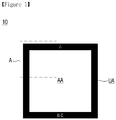
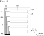
- FIG. 1 is a schematic plan view showing a touch window according to an embodiment.
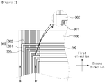
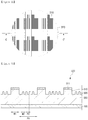
- FIG. 2 is an enlarged view of portion A of FIG. 1 .
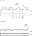
- FIG. 2 is a sectional view taken along line B-B' of FIG. 2 .
- a touch window 10 includes a substrate 100 having an active area AA, in which a position of an input device (e.g., finger) is detected, and an unactive area UA provided at a peripheral portion of the active area AA.
- an input device e.g., finger
- sensing electrodes 200 may be formed in the active area AA such that the input device may be sensed.
- a wire part 300 electrically connecting the sensing electrodes 200 may be formed in the unactive area UA.
- an external circuit connected to the wire part 300 may be placed in the unactive area UA.
- the input device such as the finger touches the touch window
- the variation of capacitance occurs in the touched part by the input device, and the touched portion subject to the variation of the capacitance may be detected as a touch point.
- the substrate 100 may include various materials to support the sensing electrode 200, a wire part 300, and a circuit substrate formed on the substrate 100.
- the substrate 100 may include a glass substrate or a plastic substrate.
- An outer dummy layer is formed in the unactive area UA of the substrate 100.
- the outer dummy layer may be coated with a material having a predetermined color so that the wire part 300 and a printed circuit board connecting the wire part 300 to external circuits cannot be viewed from the outside.
- the outer dummy layer may have a color suitable for a desired outer appearance thereof.
- the outer dummy layer includes black pigments to represent black.
- a desired logo may be formed in the outer dummy layer through various schemes.
- the outer dummy layer may be formed through deposition, print, and wet coating schemes.
- the sensing electrode 200 may be formed on the substrate 100.
- the sensing electrode 200 may detect whether the input device, such as the finger, is in contact with the sensing electrode 200.
- FIG. 2 shows the sensing electrode 200 extending in a second direction on the substrate 100, but the embodiment is not limited thereto. Accordingly, the sensing electrode 200 may extend in a first direction crossing the second direction.
- the sensing electrode 200 may comprise two types of sensing electrodes having shapes extending in the first and second directions.
- FIG. 2 shows the sensing electrode 200 having a bar shape, but the embodiment is not limited thereto. Therefore, the sensing electrode 200 may be formed in various shapes.
- the sensing electrode 200 may include a transparent conductive material such that electricity may flow therethrough without obstructing the transmission of light.
- the sensing electrode 200 may include various materials such as indium tin oxide, indium zinc oxide, copper oxide, carbon nano tube (CNT), conductive polymer or an interconnecting structure.
- the interconnecting structure may be a micro-structure having a diameter of 10 nm to 200 nm. In this case, the sensing electrode 200 may include a nanowire.
- the sensing electrode 200 may include a metallic material having superior electric conductivity.
- the sensing electrode 200 may include at least one selected from the group consisting of Cu, Au, Ag, Al, Ti, Ni and the alloy thereof.
- the electric characteristic of the touch window to which the sensing electrode 200 is applied may be improved.
- the sensing electrode 200 may include a conductive pattern. That is, the sensing electrode 200 may include a mesh shape. In this case, the sensing electrode may include various metals representing superior electric conductivity.
- FIG. 2 shows the sensing electrode 200 extending in one direction, but the embodiment is not limited thereto.
- the sensing electrode 200 may include two types of sensing electrodes consisting of one sensing electrode extending in one direction and the other sensing electrode extending in the other direction crossing the one direction.
- the one sensing electrode pattern and the other sensing electrode pattern may be variously formed according to the structure of a touch panel.
- one sensing electrode pattern and the other sensing electrode pattern may be together formed on one surface of a cover substrate.
- the one sensing electrode pattern may be formed on one surface of the cover substrate and the other sensing electrode pattern may be formed on one surface of an electrode substrate disposed on the cover substrate.
- the one sensing electrode pattern may be formed on one surface of a first electrode substrate disposed on the cover substrate and the other sensing electrode pattern may be formed on a second electrode substrate disposed on the first electrode substrate.
- the one sensing electrode pattern may be formed on one surface of a glass or film and the other sensing electrode pattern may be formed on the other surface of the glass or film.
- the touch panel according to the embodiment may have various structures according to the positions of the one sensing electrode pattern and the other sensing electrode pattern, but the embodiment is not limited thereto. That is, the one sensing electrode pattern and the other sensing electrode pattern may be formed at various positions.
- the wire part 300 electrically connecting the sensing electrode 200 may be formed in the unactive area UA.
- the wire part 300 includes first and second extending parts 301 and 302.
- the first and second extending parts 301 and 302 have mutually different directionalities. That is, the extending directions of the first and second extending parts 301 and 302 are different from each other.
- the first extending part 301 may extend in a first direction.
- the first extending part 301 may have a linear shape.
- the second extending part 302 is bent from the first extending part 301.
- the second extending part 302 may extend in a second direction crossing the first direction.
- the second extending part 302 may have a linear shape. That is, the first and second extending parts 301 and 302 may include linear lines, so that the wire part 300 does not include any curved lines. Therefore, the wire part 300 may have an 'L' shape.
- An angle ( ⁇ ) between the first and second extending parts 301 and 302 may be a right angle.
- the angle ( ⁇ ) is not necessarily required to be a right angle and may be acceptable if the angle ( ⁇ ) is within a tolerance.
- the wire parts may include a dummy pattern 320.
- the dummy pattern 320 may be diposed between two adjacent first extending parts 301.
- the dummy pattern 320 may be diposed between two adjacent second extending parts 302. That is, the dummy patterns 320 may be disposed between the first extending parts 301 or the second extending parts 302.
- the dummy pattern 320 may extend in one direction, For example, as shown in FIG. 2 , the dummy pattern 320 may extend in a first direction.
- the wire part 300 includes a main pattern 310 and a conductive layer 311. That is, each of the first and second extending parts 301 and 302 includes the main pattern 310 and the first extending part 301.
- the main pattern 310 is disposed on the substrate 100.
- the main pattern 310 may be convex.
- a line width W1 of the main pattern 310 may be in the range of 1 ⁇ m to 100 ⁇ m.
- the line width W1 of the main pattern 310 may be in the range of 5 ⁇ m to 50 ⁇ m. More preferably, the line width W1 of the main pattern 310 may be in the range of 10 ⁇ m to 30 ⁇ m.
- a distance (pitch) P1 between the main patterns 310 may be in the range of 1 ⁇ m to 100 ⁇ m.
- the distance (pitch) P1 between the main patterns 310 may be in the range of 5 ⁇ m to 50 ⁇ m. More preferably, the distance (pitch) P1 between the main patterns 310 may be in the range of 10 ⁇ m to 30 ⁇ m.
- the pitch P1 may have a demension equal to that of the line width W1.
- FIG. 3 shows the line width W1 of the main pattern 310 less than the pitch P1 for the purpose of convenience, but the line width W1 of the main pattern 310 may be equal to the pitch P1.
- the dummy pattern 320 is disposed on the substrate 100.
- the dummy pattern 320 may be disposed among the main patterns 310.
- the dummy pattern 320 may be convex.
- a line width W2 of the dummy pattern 320 may be in the range of 50 nm to 300 nm.
- a distance (pitch) P2 among the dummy patterns 320 may be equal to or less than that W2 of the dummy pattern 320.
- the main pattern 310 and the dummy pattern 320 may include resin or polymer.
- the main pattern 310 and the dummy pattern 320 may be disposed on a resin layer 350.
- the conductive layer 311 is disposed on the main pattern 310. Since the conductive layer 311 is disposed on the main pattern 310, a line width of the conductive layer 311 may be equal or similar to that of the main pattern 310.
- the line width of the conductive layer 311 may be formed in a fine pattern to have a very narrow line width, so that an area of the unactive area UA, in which the wire part 300 is disposed may be reduced.
- a touch window having a narrow bezel may be implemented. Therefore, a screen size may be ensured and variety in design may be achieved without restriction by the bezel.
- the conductive layer 311 may include a metal having superior electric conductivity.
- the conductive layer 311 may include Cu, Au, Ag, Al, Ti, Ni or the alloy thereof.
- An electrode pad (not shown) is placed at an end of the wire part 300.
- the electrode pad may be electrically connected to a printed circuit board.
- a connector is placed on one surface of the printed circuit board, and the electrode pad may be electrically connected to the connector.
- the electrode pad may be formed in a size corresponding to that of the connector.
- the printed circuit board may include various types of printed circuit boards.
- the printed circuit board may include a flexible printed circuit board (FPCB).
- FPCB flexible printed circuit board
- FIG. 4 is a sectional view showing a touch window according to the second embodiment.
- a main pattern 310 has a concave shape.
- a conductive layer 311 may be disposed in the main pattern 310. Thus, the conductive layer 311 may be prevented from being delaminated from the main pattern 310.
- a wire part 300 includes first and second extending parts 303 and 304.
- the first and second extending parts 303 and 304 have mutually different directionalities. That is, the extending directions of the first and second extending parts 301 and 302 are different from each other.
- a curve may be provided at a portion at which the first and second extending parts 303 and 304 meet each other. That is, differently from the structure of FIG. 2 described above, a line, which is not a linear line, may be provided between the first and second extending parts 303 and 304.
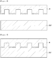
- FIGS. 6 to 10 are sectional views illustrating the method of fabricating the touch window according to the embodiment.
- the sensing electrode may be formed in the active area of the substrate in which the active and unactive areas are defined.
- a mold M having a pattern may be placed on a resin 300' which will be disposed on the unactive area.
- a resin 350' on which a pattern is formed is formed.
- the main pattern 310 and the dummy pattern 320 may be fabricated through the imprinting process.
- a conductive material 311' may be formed on the main and dummy patterns 310 and 320.
- the conductive material 311' may be formed through a deposition scheme or a plating scheme.
- the conductive materials 311' may be etched.
- a difference is made among etching areas depending on the difference among structures of the main and dummy patterns 310 and 320 and the difference among bonding areas with the electrode material 311'.
- the conductive material 311' formed on the main pattern 310 may be less etched.
- the conductive material 311' formed on the main pattern 310 remains, and the conductive material 311' formed on the dummy pattern 320 is etched and removed. Therefore, the conductive layer 311 may be formed only on the main pattern 310.
- the first and second extending parts 301 and 302 constituting the main pattern 310 may be perpendicular to each other, so that any residual conductive materials 311' that remain without being etch may not etch at any portions except for the main pattern 310. That is, any portions except from the main pattern 310 may be prevented from being non-etched.
- the wire part 300 for electrically connecting the sensing electrode 200 may be formed in the unactive area UA.
- the wire part 300 may include the main pattern 310, the dummy pattern 320 and the conductive layer 311.
- the main pattern 310 is disposed on the substrate 100.
- the main pattern 310 may be convex.
- a line width W1 of the main pattern 310 may be in the range of 1 ⁇ m to 100 ⁇ m.
- the line width W1 of the main pattern 310 may be in the range of 5 ⁇ m to 50 ⁇ m . More preferably, the line width W1 of the main pattern 310 may be in the range of 10 ⁇ m to 30 ⁇ m.
- a distance (pitch) P1 between the main patterns 310 may be in the range of 1 ⁇ m to 100 ⁇ m.
- the distance (pitch) P1 between the main patterns 310 may be in the range of 5 ⁇ m to 50 ⁇ m. More preferably, the distance (pitch) PI between the main patterns 310 may be in the range of 10 ⁇ m to 30 ⁇ m.
- the pitch P1 may have a dimension equal to that of the line width W1.
- FIG. 13 shows the line width W1 of the main pattern 310 less than the pitch P1 for the purpose of convenience, but the line width W1 of the main pattern 310 may be equal to the pitch P1.
- the dummy pattern 320 is disposed on the substrate 100.
- the dummy pattern 320 may be disposed among the main patterns 310.
- the dummy pattern 320 may be convex.
- a line width W2 of the dummy pattern 320 may be in the range of 50 nm to 300 nm.
- a distance (pitch) P2 among the dummy patterns 320 may be equal to or less than that W2 of the dummy pattern 320.
- the main pattern 310 and the dummy pattern 320 may include resin or polymer.
- the conductive layer 311 is disposed on the main pattern 310. Since the conductive layer 311 is disposed on the main pattern 310, a line width of the conductive layer 311 may be equal or similar to that of the main pattern 310.
- the line width of the conductive layer 311 may be formed in a fine pattern to have a very narrow line width, so that an area of the unactive area UA, in which the wire part 300 is disposed may be reduced.
- a touch window having a narrow bezel may be implemented. Therefore, a screen size may be ensured and variety in design may be achieved without restriction by the bezel.
- the conductive layer 311 may include a metal having superior electric conductivity.
- the conductive layer 311 may include Cu, Au, Ag, Al, Ti, Ni or the alloy thereof.
- the main pattern 310 includes first and second extending parts 301 and 302.
- the first extending part 301 may extend in a first direction.
- the first extending part 301 may have a linear shape.
- the second extending part 302 is bent from the first extending part 301.
- the second extending part 302 may extend in a second direction crossing the first direction.
- the second extending part 302 may have a linear shape.
- the first and second extending parts 301 and 302 may be perpendicular to each other.
- a dummy pattern 320 may be disposed adjacent to the first and second extending parts 301 and 302.
- the dummy pattern 320 may be diposed between two adjacent first extending parts 301.
- the dummy pattern 320 may be diposed between two adjacent second extending parts 302. That is, the dummy patterns 320 may be disposed between the first extending parts 301 or the second extending parts 302.
- the dummy pattern 320 may extend in one direction.
- the dummy pattern 320 may extend in a first direction.
- An electrode pad 400 is placed at an end of the wire part 300.
- the electrode pad 400 may be electrically connected to a printed circuit board.
- a connector is placed on one surface of the printed circuit board, and the electrode pad 400 may be electrically connected to the connector.
- the electrode pad 400 may be formed in a size corresponding to that of the connector.
- the printed circuit board may include various types of printed circuit boards.
- the printed circuit board may include a flexible printed circuit board (FPCB).
- FPCB flexible printed circuit board
- FIG. 15 a touch window according to another embodiment will be described with reference to FIG. 15 .
- the details about the same or similar portions will be omitted for the purpose of brief explanation or clarity.
- a main pattern 310 has a concave shape.
- a conductive layer 311 may be disposed in the main pattern 310. Thus, the conductive layer 311 may be prevented from being delaminated from the main pattern 310.
- an end 311e of the electrode layer 311 disposed on the main pattern 310 may be disposed on a portion of a side surface 310e of the main pattern 310. That is, the electrode layer 311 may be disposed as if it surrounds the main pattern 310. In this case, the end 311e of the electrode layer 311 may make direct-contact with or be spaced apart from the side surface 310e of the main pattern 310.
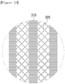
- the dummy pattern 323 may be disposed to cross the main pattern 313. That is, differently from the embodiment shown in FIG. 12 , the main pattern 313 may not be parallel to the dummy pattern 323.
- the dummy pattern 325 may be disposed to have a mesh shape.
- the conductive materials formed on the dummy patterns 323 and 325 may be easily etched.
- the conductive material may remain only on the main pattern 313.
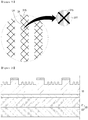
- the main pattern 315 may include a conductive pattern. That is, the main pattern 315 may be disposed in a mesh shape.
- the main pattern 315 may include a mesh opening OA and a mesh line LA.
- a line width of the mesh line LA may be in the range of 0.1 ⁇ m to 10 ⁇ m.
- the forming of a mesh line LA having a line width of 0.1 ⁇ m or less may be impossible in the fabricating process. If the line width is 10 ⁇ m or less, the pattern of the electrode layer may not be viewed.
- the line width of the mesh line LA may be in the range of 1 ⁇ m to 7 ⁇ m. More preferably, the line width of the mesh line LA may be in the range of 2 ⁇ m to 5 ⁇ m.
- the mesh opening OA may have the shape of a rectangular shape, but the embodiment is not limited thereto.
- the mesh opening OA may have various shapes such as a polygonal shape including a diamond shape, a pentagonal shape or a hexagonal shape, or a circular shape and may be disposed regularly. That is, the conductive pattern may have a regular shape.
- the embodiment is not limited to the above, and the conductive pattern may have an irregular shape. That is, conductive pattern openings may be variously provided in one conductive pattern.
- the dummy pattern 327 is disposed adjacently to the main pattern 315.
- the dummy patterns 327 may be disposed among the main patterns 315.
- the dummy pattern 327 is disposed in the mesh opening OA.
- the touch window 10 may be disposed on a display panel 20 which is a driving unit.
- the touch window 10 is combined with the display panel 20 so that a touch device may be formed.
- the display panel 20 is formed therein with a display region to display an image.
- the display panel applied to the display device may include an upper substrate 21 and a lower substrate 22.
- a data line, a gate line, and a thin film transistor TFT may be formed on the lower substrate 22.
- the upper substrate 21 may adhere to the lower substrate 22 to protect constituent elements disposed on the lower substrate 22.
- the display panel 20 may be formed in various types according to a kind of the touch device. That is, the touch device according to the embodiment may include an LCD, a field emission display, a plasma display panel (PDP), an organic light emitting diode (OLED), and an electrophoretic display (EPD). Accordingly, the touch panel 20 may be configured in various types.
- the touch device may include an LCD, a field emission display, a plasma display panel (PDP), an organic light emitting diode (OLED), and an electrophoretic display (EPD). Accordingly, the touch panel 20 may be configured in various types.
- the touch window may be applied to a vehicle as well as a touch device of a mobile terminal.
- the touch window may be applied to a personal navigation display (PND) such as vehicle navigation.
- the touch window may be applied to a dashboard such that a center information display (CID) may be implemented.
- PND personal navigation display
- CID center information display
- the embodiment is not limited to the above, and the touch device may be used for various electronic appliances.
Landscapes
- Engineering & Computer Science (AREA)
- Theoretical Computer Science (AREA)
- General Engineering & Computer Science (AREA)
- Physics & Mathematics (AREA)
- General Physics & Mathematics (AREA)
- Human Computer Interaction (AREA)
- Computer Hardware Design (AREA)
- Computer Networks & Wireless Communication (AREA)
- Position Input By Displaying (AREA)
Claims (15)
- Fenêtre tactile comprenant :un substrat (100) ayant une zone active, dans laquelle une position d'un dispositif d'entrée est détectée, et une zone inactive prévue au niveau d'une portion périphérique de la zone active ;une électrode de détection (200) disposée sur la zone active du substrat (100) pour détecter une position ; des parties de fil (300) pour connecter électriquement l'électrode de détection (200), dans laquelle les parties de fil (300) sont disposées sur la zone inactive du substrat ; etun circuit externe aux parties de fil disposées sur la zone inactive du substrat,caractérisée en ce que les parties de fil (300) comportent des premières parties d'extension (301 ; 303) et des secondes parties d'extension (302 ; 304) ayant des directionnalités mutuellement différentes,dans laquelle les parties de fil (300) comportent un motif factice (320 ; 323 ; 325 ; 327) disposé entre les premières parties d'extension (301 ; 303) ou entre les secondes parties d'extension (302 ; 304),dans laquelle les parties de fil (300) comportent un motif principal (310 ; 313 ; 315) et le motif factice (320 ; 323 ; 325 ; 327) adjacent au motif principal (310 ; 313 ; 315), et une couche conductrice (311) sur le motif principal (310 ; 313 ; 315),dans laquelle une largeur de ligne du motif principal (310 ; 313 ; 315) est supérieure à une largeur de ligne du motif factice (320 ; 323 ; 325 ; 327) .
- Fenêtre tactile selon la revendication 1, dans laquelle le motif principal (310 ; 313 ; 315) est convexe ou concave.
- Fenêtre tactile selon l'une quelconque des revendications 1 ou 2, dans laquelle un angle entre les premières et secondes parties d'extension est un angle droit.
- Fenêtre tactile selon la revendication 3, dans laquelle le motif factice (320 ; 323 ; 325 ; 327) est disposé entre les premières parties d'extension (301 ; 303) ou entre les secondes parties d'extension (302 ; 304) .
- Fenêtre tactile selon la revendication 1, dans laquelle le motif factice (320 ; 323 ; 325 ; 327) s'étend dans une direction.
- Fenêtre tactile selon l'une quelconque des revendications 1 à 5, dans laquelle la couche conductrice (311) comporte du Cu, Au, Ag, Al, Ti, Ni ou un alliage de ceux-ci.
- Fenêtre tactile selon la revendication 6, dans laquelle une extrémité (311e) de la couche conductrice (311) disposée sur le motif principal (310) est disposée sur une portion d'une surface de côté (310e) du motif principal (310).
- Fenêtre tactile selon l'une quelconque des revendications 1 à 7, dans laquelle le motif principal (310 ; 313 ; 315) comporte un motif conducteur.
- Fenêtre tactile selon la revendication 8, dans laquelle une largeur de ligne du motif conducteur du motif principal (310 ; 313 ; 315) est dans une plage de 0,5 µm à 5 µm.
- Fenêtre tactile selon l'une quelconque des revendications 8 ou 9, dans laquelle une largeur de ligne du motif conducteur du motif principal (310 ; 313 ; 315) est supérieure à une largeur de ligne du motif factice (320 ; 323 ; 325 ; 327).
- Fenêtre tactile selon la revendication 1, dans laquelle le motif principal (310 ; 313 ; 315) n'est pas parallèle au motif factice (320 ; 323 ; 325 ; 327).
- Fenêtre tactile selon la revendication 1, dans laquelle le motif principal (310 ; 313 ; 315) et le motif factice (320 ; 323 ; 325 ; 327) comportent une résine.
- Fenêtre tactile selon la revendication 1, dans laquelle le motif factice (320 ; 323 ; 325 ; 327) est disposé en une forme de maille.
- Fenêtre tactile selon la revendication 1, dans laquelle la largeur de ligne du motif principal est dans la plage de 1 µm à 100 µm, et
dans laquelle la largeur de ligne du motif factice est dans une plage de 50 nm à 300 nm. - Fenêtre tactile selon la revendication 1, dans laquelle la fenêtre tactile (10) est une fenêtre tactile sur un panneau d'affichage (20) faisant partie d'un dispositif tactile.
Applications Claiming Priority (2)
| Application Number | Priority Date | Filing Date | Title |
|---|---|---|---|
| KR20130089660 | 2013-07-29 | ||
| KR20130089662 | 2013-07-29 |
Publications (2)
| Publication Number | Publication Date |
|---|---|
| EP2833246A1 EP2833246A1 (fr) | 2015-02-04 |
| EP2833246B1 true EP2833246B1 (fr) | 2018-06-27 |
Family
ID=51357714
Family Applications (1)
| Application Number | Title | Priority Date | Filing Date |
|---|---|---|---|
| EP14178686.3A Not-in-force EP2833246B1 (fr) | 2013-07-29 | 2014-07-28 | Fenêtre tactile et dispositif tactile la comprenant |
Country Status (4)
| Country | Link |
|---|---|
| US (1) | US9618982B2 (fr) |
| EP (1) | EP2833246B1 (fr) |
| CN (1) | CN104345976B (fr) |
| TW (1) | TW201506753A (fr) |
Families Citing this family (8)
| Publication number | Priority date | Publication date | Assignee | Title |
|---|---|---|---|---|
| FR3014573B1 (fr) * | 2013-12-11 | 2016-12-23 | Valeo Systemes Thermiques | Dispositif de commande tactile |
| TWI610204B (zh) * | 2015-02-27 | 2018-01-01 | Fujikura Ltd | 配線體、配線基板以及碰觸偵知器 |
| KR102306654B1 (ko) * | 2015-04-27 | 2021-09-29 | 삼성디스플레이 주식회사 | 터치 패널 |
| CN106293287B (zh) * | 2015-06-10 | 2023-09-22 | 宸鸿科技(厦门)有限公司 | 具指纹辨识功能的触控装置 |
| JP7059042B2 (ja) | 2018-01-10 | 2022-04-25 | 株式会社ワコム | センサパネル |
| KR102837449B1 (ko) * | 2019-07-12 | 2025-07-24 | 삼성디스플레이 주식회사 | 입력 감지 유닛 및 이를 포함하는 표시모듈 |
| KR102792453B1 (ko) * | 2020-08-14 | 2025-04-08 | 삼성전자주식회사 | 안테나 및 그것을 포함하는 전자 장치 |
| CN117456831B (zh) * | 2022-07-25 | 2026-01-27 | 京东方科技集团股份有限公司 | 显示面板及其制备方法和显示装置 |
Family Cites Families (12)
| Publication number | Priority date | Publication date | Assignee | Title |
|---|---|---|---|---|
| US8421757B2 (en) * | 2007-10-12 | 2013-04-16 | Sony Corporation | Touch sensor with a plurality of touch sensor sections |
| KR101641957B1 (ko) | 2008-11-24 | 2016-07-25 | 삼성디스플레이 주식회사 | 패턴 형성 방법, 이를 이용하여 제조한 표시 기판 및 표시 장치 |
| US8269744B2 (en) * | 2008-09-05 | 2012-09-18 | Mitsubishi Electric Corporation | Touch screen, touch panel and display device |
| JP2012236276A (ja) | 2009-09-18 | 2012-12-06 | Pilot Ink Co Ltd | ボールペンチップ及びボールペンチップの製造方法 |
| KR101710552B1 (ko) * | 2010-07-20 | 2017-02-28 | 삼성디스플레이 주식회사 | 터치 스크린 패널 |
| JP5670827B2 (ja) * | 2011-05-13 | 2015-02-18 | 富士フイルム株式会社 | 導電シート及びタッチパネル |
| KR101447738B1 (ko) * | 2011-05-26 | 2014-10-06 | 엘지이노텍 주식회사 | 터치윈도우 |
| KR101303635B1 (ko) | 2011-05-26 | 2013-09-11 | 엘지이노텍 주식회사 | 터치윈도우 |
| KR101327310B1 (ko) | 2011-07-06 | 2013-11-11 | (재)한국나노기술원 | 임프린트 리소그래피와 다층 박막을 이용한 패터닝 방법 |
| KR101368994B1 (ko) | 2011-08-03 | 2014-02-28 | 박준영 | 터치 패널용 패드의 제조 방법 |
| JP5809117B2 (ja) * | 2011-10-05 | 2015-11-10 | 富士フイルム株式会社 | 導電シート、タッチパネル、表示装置 |
| KR20130078065A (ko) * | 2011-12-30 | 2013-07-10 | 삼성전기주식회사 | 터치패널 |
-
2014
- 2014-07-15 TW TW103124244A patent/TW201506753A/zh unknown
- 2014-07-28 EP EP14178686.3A patent/EP2833246B1/fr not_active Not-in-force
- 2014-07-29 US US14/446,001 patent/US9618982B2/en not_active Expired - Fee Related
- 2014-07-29 CN CN201410367458.0A patent/CN104345976B/zh not_active Expired - Fee Related
Non-Patent Citations (1)
| Title |
|---|
| None * |
Also Published As
| Publication number | Publication date |
|---|---|
| US9618982B2 (en) | 2017-04-11 |
| EP2833246A1 (fr) | 2015-02-04 |
| CN104345976B (zh) | 2019-05-21 |
| TW201506753A (zh) | 2015-02-16 |
| CN104345976A (zh) | 2015-02-11 |
| US20150028897A1 (en) | 2015-01-29 |
Similar Documents
| Publication | Publication Date | Title |
|---|---|---|
| US11340741B2 (en) | Touch window having a sensing electrode with a variable width of a conductive line | |
| EP2833246B1 (fr) | Fenêtre tactile et dispositif tactile la comprenant | |
| US10156944B2 (en) | Touch window | |
| EP2827231B1 (fr) | Fenêtre tactile et affichage la comprenant | |
| EP2784639B1 (fr) | Panneau tactile et dispositif tactile l'utilisant | |
| CN104423708B (zh) | 触摸窗及包括触摸窗的触控装置 | |
| US10521048B2 (en) | Touch window and touch device including the same | |
| US10191590B2 (en) | Touch window | |
| US10025421B2 (en) | Touch window | |
| EP2833235B1 (fr) | Panneau tactile flexible avec surface active pliable | |
| US10055074B2 (en) | Touch window | |
| KR20150014375A (ko) | 터치 윈도우 및 이의 제조방법 | |
| KR102187787B1 (ko) | 터치 윈도우 | |
| KR102380881B1 (ko) | 터치 윈도우 | |
| KR20170001328A (ko) | 터치 윈도우 | |
| KR20150014376A (ko) | 터치 윈도우 및 이를 포함하는 터치 디바이스 | |
| KR20170001053A (ko) | 터치 윈도우 | |
| KR20160092372A (ko) | 터치 윈도우 | |
| KR20170039391A (ko) | 터치 윈도우 |
Legal Events
| Date | Code | Title | Description |
|---|---|---|---|
| 17P | Request for examination filed |
Effective date: 20140728 |
|
| AK | Designated contracting states |
Kind code of ref document: A1 Designated state(s): AL AT BE BG CH CY CZ DE DK EE ES FI FR GB GR HR HU IE IS IT LI LT LU LV MC MK MT NL NO PL PT RO RS SE SI SK SM TR |
|
| AX | Request for extension of the european patent |
Extension state: BA ME |
|
| PUAI | Public reference made under article 153(3) epc to a published international application that has entered the european phase |
Free format text: ORIGINAL CODE: 0009012 |
|
| R17P | Request for examination filed (corrected) |
Effective date: 20150731 |
|
| RBV | Designated contracting states (corrected) |
Designated state(s): AL AT BE BG CH CY CZ DE DK EE ES FI FR GB GR HR HU IE IS IT LI LT LU LV MC MK MT NL NO PL PT RO RS SE SI SK SM TR |
|
| 17Q | First examination report despatched |
Effective date: 20160307 |
|
| STAA | Information on the status of an ep patent application or granted ep patent |
Free format text: STATUS: EXAMINATION IS IN PROGRESS |
|
| RAP1 | Party data changed (applicant data changed or rights of an application transferred) |
Owner name: LG INNOTEK CO., LTD. |
|
| GRAP | Despatch of communication of intention to grant a patent |
Free format text: ORIGINAL CODE: EPIDOSNIGR1 |
|
| STAA | Information on the status of an ep patent application or granted ep patent |
Free format text: STATUS: GRANT OF PATENT IS INTENDED |
|
| RIC1 | Information provided on ipc code assigned before grant |
Ipc: G06F 1/16 20060101ALI20180116BHEP Ipc: G01R 27/26 20060101ALI20180116BHEP Ipc: G06F 3/041 20060101AFI20180116BHEP Ipc: G06F 3/044 20060101ALI20180116BHEP |
|
| INTG | Intention to grant announced |
Effective date: 20180208 |
|
| GRAS | Grant fee paid |
Free format text: ORIGINAL CODE: EPIDOSNIGR3 |
|
| GRAA | (expected) grant |
Free format text: ORIGINAL CODE: 0009210 |
|
| STAA | Information on the status of an ep patent application or granted ep patent |
Free format text: STATUS: THE PATENT HAS BEEN GRANTED |
|
| AK | Designated contracting states |
Kind code of ref document: B1 Designated state(s): AL AT BE BG CH CY CZ DE DK EE ES FI FR GB GR HR HU IE IS IT LI LT LU LV MC MK MT NL NO PL PT RO RS SE SI SK SM TR |
|
| REG | Reference to a national code |
Ref country code: GB Ref legal event code: FG4D |
|
| REG | Reference to a national code |
Ref country code: AT Ref legal event code: REF Ref document number: 1012886 Country of ref document: AT Kind code of ref document: T Effective date: 20180715 |
|
| REG | Reference to a national code |
Ref country code: IE Ref legal event code: FG4D |
|
| REG | Reference to a national code |
Ref country code: DE Ref legal event code: R096 Ref document number: 602014027461 Country of ref document: DE |
|
| PG25 | Lapsed in a contracting state [announced via postgrant information from national office to epo] |
Ref country code: LT Free format text: LAPSE BECAUSE OF FAILURE TO SUBMIT A TRANSLATION OF THE DESCRIPTION OR TO PAY THE FEE WITHIN THE PRESCRIBED TIME-LIMIT Effective date: 20180627 Ref country code: NO Free format text: LAPSE BECAUSE OF FAILURE TO SUBMIT A TRANSLATION OF THE DESCRIPTION OR TO PAY THE FEE WITHIN THE PRESCRIBED TIME-LIMIT Effective date: 20180927 Ref country code: SE Free format text: LAPSE BECAUSE OF FAILURE TO SUBMIT A TRANSLATION OF THE DESCRIPTION OR TO PAY THE FEE WITHIN THE PRESCRIBED TIME-LIMIT Effective date: 20180627 Ref country code: BG Free format text: LAPSE BECAUSE OF FAILURE TO SUBMIT A TRANSLATION OF THE DESCRIPTION OR TO PAY THE FEE WITHIN THE PRESCRIBED TIME-LIMIT Effective date: 20180927 Ref country code: FI Free format text: LAPSE BECAUSE OF FAILURE TO SUBMIT A TRANSLATION OF THE DESCRIPTION OR TO PAY THE FEE WITHIN THE PRESCRIBED TIME-LIMIT Effective date: 20180627 |
|
| REG | Reference to a national code |
Ref country code: NL Ref legal event code: MP Effective date: 20180627 |
|
| REG | Reference to a national code |
Ref country code: LT Ref legal event code: MG4D |
|
| PG25 | Lapsed in a contracting state [announced via postgrant information from national office to epo] |
Ref country code: RS Free format text: LAPSE BECAUSE OF FAILURE TO SUBMIT A TRANSLATION OF THE DESCRIPTION OR TO PAY THE FEE WITHIN THE PRESCRIBED TIME-LIMIT Effective date: 20180627 Ref country code: LV Free format text: LAPSE BECAUSE OF FAILURE TO SUBMIT A TRANSLATION OF THE DESCRIPTION OR TO PAY THE FEE WITHIN THE PRESCRIBED TIME-LIMIT Effective date: 20180627 Ref country code: HR Free format text: LAPSE BECAUSE OF FAILURE TO SUBMIT A TRANSLATION OF THE DESCRIPTION OR TO PAY THE FEE WITHIN THE PRESCRIBED TIME-LIMIT Effective date: 20180627 Ref country code: GR Free format text: LAPSE BECAUSE OF FAILURE TO SUBMIT A TRANSLATION OF THE DESCRIPTION OR TO PAY THE FEE WITHIN THE PRESCRIBED TIME-LIMIT Effective date: 20180928 |
|
| REG | Reference to a national code |
Ref country code: AT Ref legal event code: MK05 Ref document number: 1012886 Country of ref document: AT Kind code of ref document: T Effective date: 20180627 |
|
| PG25 | Lapsed in a contracting state [announced via postgrant information from national office to epo] |
Ref country code: NL Free format text: LAPSE BECAUSE OF FAILURE TO SUBMIT A TRANSLATION OF THE DESCRIPTION OR TO PAY THE FEE WITHIN THE PRESCRIBED TIME-LIMIT Effective date: 20180627 |
|
| PG25 | Lapsed in a contracting state [announced via postgrant information from national office to epo] |
Ref country code: IS Free format text: LAPSE BECAUSE OF FAILURE TO SUBMIT A TRANSLATION OF THE DESCRIPTION OR TO PAY THE FEE WITHIN THE PRESCRIBED TIME-LIMIT Effective date: 20181027 Ref country code: AT Free format text: LAPSE BECAUSE OF FAILURE TO SUBMIT A TRANSLATION OF THE DESCRIPTION OR TO PAY THE FEE WITHIN THE PRESCRIBED TIME-LIMIT Effective date: 20180627 Ref country code: EE Free format text: LAPSE BECAUSE OF FAILURE TO SUBMIT A TRANSLATION OF THE DESCRIPTION OR TO PAY THE FEE WITHIN THE PRESCRIBED TIME-LIMIT Effective date: 20180627 Ref country code: RO Free format text: LAPSE BECAUSE OF FAILURE TO SUBMIT A TRANSLATION OF THE DESCRIPTION OR TO PAY THE FEE WITHIN THE PRESCRIBED TIME-LIMIT Effective date: 20180627 Ref country code: SK Free format text: LAPSE BECAUSE OF FAILURE TO SUBMIT A TRANSLATION OF THE DESCRIPTION OR TO PAY THE FEE WITHIN THE PRESCRIBED TIME-LIMIT Effective date: 20180627 Ref country code: PL Free format text: LAPSE BECAUSE OF FAILURE TO SUBMIT A TRANSLATION OF THE DESCRIPTION OR TO PAY THE FEE WITHIN THE PRESCRIBED TIME-LIMIT Effective date: 20180627 Ref country code: CZ Free format text: LAPSE BECAUSE OF FAILURE TO SUBMIT A TRANSLATION OF THE DESCRIPTION OR TO PAY THE FEE WITHIN THE PRESCRIBED TIME-LIMIT Effective date: 20180627 |
|
| PG25 | Lapsed in a contracting state [announced via postgrant information from national office to epo] |
Ref country code: ES Free format text: LAPSE BECAUSE OF FAILURE TO SUBMIT A TRANSLATION OF THE DESCRIPTION OR TO PAY THE FEE WITHIN THE PRESCRIBED TIME-LIMIT Effective date: 20180627 Ref country code: IT Free format text: LAPSE BECAUSE OF FAILURE TO SUBMIT A TRANSLATION OF THE DESCRIPTION OR TO PAY THE FEE WITHIN THE PRESCRIBED TIME-LIMIT Effective date: 20180627 Ref country code: SM Free format text: LAPSE BECAUSE OF FAILURE TO SUBMIT A TRANSLATION OF THE DESCRIPTION OR TO PAY THE FEE WITHIN THE PRESCRIBED TIME-LIMIT Effective date: 20180627 |
|
| REG | Reference to a national code |
Ref country code: CH Ref legal event code: PL |
|
| REG | Reference to a national code |
Ref country code: DE Ref legal event code: R097 Ref document number: 602014027461 Country of ref document: DE |
|
| PG25 | Lapsed in a contracting state [announced via postgrant information from national office to epo] |
Ref country code: LU Free format text: LAPSE BECAUSE OF NON-PAYMENT OF DUE FEES Effective date: 20180728 Ref country code: MC Free format text: LAPSE BECAUSE OF FAILURE TO SUBMIT A TRANSLATION OF THE DESCRIPTION OR TO PAY THE FEE WITHIN THE PRESCRIBED TIME-LIMIT Effective date: 20180627 |
|
| REG | Reference to a national code |
Ref country code: BE Ref legal event code: MM Effective date: 20180731 |
|
| PG25 | Lapsed in a contracting state [announced via postgrant information from national office to epo] |
Ref country code: CH Free format text: LAPSE BECAUSE OF NON-PAYMENT OF DUE FEES Effective date: 20180731 Ref country code: LI Free format text: LAPSE BECAUSE OF NON-PAYMENT OF DUE FEES Effective date: 20180731 |
|
| REG | Reference to a national code |
Ref country code: IE Ref legal event code: MM4A |
|
| PLBE | No opposition filed within time limit |
Free format text: ORIGINAL CODE: 0009261 |
|
| STAA | Information on the status of an ep patent application or granted ep patent |
Free format text: STATUS: NO OPPOSITION FILED WITHIN TIME LIMIT |
|
| GBPC | Gb: european patent ceased through non-payment of renewal fee |
Effective date: 20180927 |
|
| PG25 | Lapsed in a contracting state [announced via postgrant information from national office to epo] |
Ref country code: BE Free format text: LAPSE BECAUSE OF NON-PAYMENT OF DUE FEES Effective date: 20180731 Ref country code: DK Free format text: LAPSE BECAUSE OF FAILURE TO SUBMIT A TRANSLATION OF THE DESCRIPTION OR TO PAY THE FEE WITHIN THE PRESCRIBED TIME-LIMIT Effective date: 20180627 |
|
| 26N | No opposition filed |
Effective date: 20190328 |
|
| PG25 | Lapsed in a contracting state [announced via postgrant information from national office to epo] |
Ref country code: IE Free format text: LAPSE BECAUSE OF NON-PAYMENT OF DUE FEES Effective date: 20180728 |
|
| PG25 | Lapsed in a contracting state [announced via postgrant information from national office to epo] |
Ref country code: SI Free format text: LAPSE BECAUSE OF FAILURE TO SUBMIT A TRANSLATION OF THE DESCRIPTION OR TO PAY THE FEE WITHIN THE PRESCRIBED TIME-LIMIT Effective date: 20180627 Ref country code: FR Free format text: LAPSE BECAUSE OF NON-PAYMENT OF DUE FEES Effective date: 20180827 |
|
| PG25 | Lapsed in a contracting state [announced via postgrant information from national office to epo] |
Ref country code: GB Free format text: LAPSE BECAUSE OF NON-PAYMENT OF DUE FEES Effective date: 20180927 |
|
| PGFP | Annual fee paid to national office [announced via postgrant information from national office to epo] |
Ref country code: DE Payment date: 20190604 Year of fee payment: 6 |
|
| PG25 | Lapsed in a contracting state [announced via postgrant information from national office to epo] |
Ref country code: AL Free format text: LAPSE BECAUSE OF FAILURE TO SUBMIT A TRANSLATION OF THE DESCRIPTION OR TO PAY THE FEE WITHIN THE PRESCRIBED TIME-LIMIT Effective date: 20180627 |
|
| PG25 | Lapsed in a contracting state [announced via postgrant information from national office to epo] |
Ref country code: MT Free format text: LAPSE BECAUSE OF NON-PAYMENT OF DUE FEES Effective date: 20180728 |
|
| PG25 | Lapsed in a contracting state [announced via postgrant information from national office to epo] |
Ref country code: TR Free format text: LAPSE BECAUSE OF FAILURE TO SUBMIT A TRANSLATION OF THE DESCRIPTION OR TO PAY THE FEE WITHIN THE PRESCRIBED TIME-LIMIT Effective date: 20180627 |
|
| PG25 | Lapsed in a contracting state [announced via postgrant information from national office to epo] |
Ref country code: HU Free format text: LAPSE BECAUSE OF FAILURE TO SUBMIT A TRANSLATION OF THE DESCRIPTION OR TO PAY THE FEE WITHIN THE PRESCRIBED TIME-LIMIT; INVALID AB INITIO Effective date: 20140728 Ref country code: PT Free format text: LAPSE BECAUSE OF FAILURE TO SUBMIT A TRANSLATION OF THE DESCRIPTION OR TO PAY THE FEE WITHIN THE PRESCRIBED TIME-LIMIT Effective date: 20180627 |
|
| PG25 | Lapsed in a contracting state [announced via postgrant information from national office to epo] |
Ref country code: CY Free format text: LAPSE BECAUSE OF FAILURE TO SUBMIT A TRANSLATION OF THE DESCRIPTION OR TO PAY THE FEE WITHIN THE PRESCRIBED TIME-LIMIT Effective date: 20180627 Ref country code: MK Free format text: LAPSE BECAUSE OF NON-PAYMENT OF DUE FEES Effective date: 20180627 |
|
| REG | Reference to a national code |
Ref country code: DE Ref legal event code: R119 Ref document number: 602014027461 Country of ref document: DE |
|
| PG25 | Lapsed in a contracting state [announced via postgrant information from national office to epo] |
Ref country code: DE Free format text: LAPSE BECAUSE OF NON-PAYMENT OF DUE FEES Effective date: 20210202 |