EP2833406B1 - Abbildungselement und abbildungsvorrichtung - Google Patents
Abbildungselement und abbildungsvorrichtung Download PDFInfo
- Publication number
- EP2833406B1 EP2833406B1 EP13769765.2A EP13769765A EP2833406B1 EP 2833406 B1 EP2833406 B1 EP 2833406B1 EP 13769765 A EP13769765 A EP 13769765A EP 2833406 B1 EP2833406 B1 EP 2833406B1
- Authority
- EP
- European Patent Office
- Prior art keywords
- pixel cell
- detects
- light component
- imaging element
- pixel
- Prior art date
- Legal status (The legal status is an assumption and is not a legal conclusion. Google has not performed a legal analysis and makes no representation as to the accuracy of the status listed.)
- Not-in-force
Links
Images





Classifications
-
- H—ELECTRICITY
- H04—ELECTRIC COMMUNICATION TECHNIQUE
- H04N—PICTORIAL COMMUNICATION, e.g. TELEVISION
- H04N25/00—Circuitry of solid-state image sensors [SSIS]; Control thereof
- H04N25/10—Circuitry of solid-state image sensors [SSIS]; Control thereof for transforming different wavelengths into image signals
- H04N25/11—Arrangement of colour filter arrays [CFA]; Filter mosaics
- H04N25/13—Arrangement of colour filter arrays [CFA]; Filter mosaics characterised by the spectral characteristics of the filter elements
- H04N25/134—Arrangement of colour filter arrays [CFA]; Filter mosaics characterised by the spectral characteristics of the filter elements based on three different wavelength filter elements
-
- H—ELECTRICITY
- H04—ELECTRIC COMMUNICATION TECHNIQUE
- H04N—PICTORIAL COMMUNICATION, e.g. TELEVISION
- H04N13/00—Stereoscopic video systems; Multi-view video systems; Details thereof
- H04N13/20—Image signal generators
- H04N13/257—Colour aspects
-
- H—ELECTRICITY
- H04—ELECTRIC COMMUNICATION TECHNIQUE
- H04N—PICTORIAL COMMUNICATION, e.g. TELEVISION
- H04N23/00—Cameras or camera modules comprising electronic image sensors; Control thereof
- H04N23/60—Control of cameras or camera modules
- H04N23/67—Focus control based on electronic image sensor signals
- H04N23/672—Focus control based on electronic image sensor signals based on the phase difference signals
-
- H—ELECTRICITY
- H04—ELECTRIC COMMUNICATION TECHNIQUE
- H04N—PICTORIAL COMMUNICATION, e.g. TELEVISION
- H04N25/00—Circuitry of solid-state image sensors [SSIS]; Control thereof
- H04N25/70—SSIS architectures; Circuits associated therewith
- H04N25/703—SSIS architectures incorporating pixels for producing signals other than image signals
- H04N25/704—Pixels specially adapted for focusing, e.g. phase difference pixel sets
-
- H—ELECTRICITY
- H04—ELECTRIC COMMUNICATION TECHNIQUE
- H04N—PICTORIAL COMMUNICATION, e.g. TELEVISION
- H04N9/00—Details of colour television systems
- H04N9/77—Circuits for processing the brightness signal and the chrominance signal relative to each other, e.g. adjusting the phase of the brightness signal relative to the colour signal, correcting differential gain or differential phase
-
- H—ELECTRICITY
- H10—SEMICONDUCTOR DEVICES; ELECTRIC SOLID-STATE DEVICES NOT OTHERWISE PROVIDED FOR
- H10F—INORGANIC SEMICONDUCTOR DEVICES SENSITIVE TO INFRARED RADIATION, LIGHT, ELECTROMAGNETIC RADIATION OF SHORTER WAVELENGTH OR CORPUSCULAR RADIATION
- H10F39/00—Integrated devices, or assemblies of multiple devices, comprising at least one element covered by group H10F30/00, e.g. radiation detectors comprising photodiode arrays
- H10F39/80—Constructional details of image sensors
- H10F39/802—Geometry or disposition of elements in pixels, e.g. address-lines or gate electrodes
- H10F39/8023—Disposition of the elements in pixels, e.g. smaller elements in the centre of the imager compared to larger elements at the periphery
-
- H—ELECTRICITY
- H10—SEMICONDUCTOR DEVICES; ELECTRIC SOLID-STATE DEVICES NOT OTHERWISE PROVIDED FOR
- H10F—INORGANIC SEMICONDUCTOR DEVICES SENSITIVE TO INFRARED RADIATION, LIGHT, ELECTROMAGNETIC RADIATION OF SHORTER WAVELENGTH OR CORPUSCULAR RADIATION
- H10F39/00—Integrated devices, or assemblies of multiple devices, comprising at least one element covered by group H10F30/00, e.g. radiation detectors comprising photodiode arrays
- H10F39/80—Constructional details of image sensors
- H10F39/805—Coatings
- H10F39/8053—Colour filters
-
- H—ELECTRICITY
- H10—SEMICONDUCTOR DEVICES; ELECTRIC SOLID-STATE DEVICES NOT OTHERWISE PROVIDED FOR
- H10F—INORGANIC SEMICONDUCTOR DEVICES SENSITIVE TO INFRARED RADIATION, LIGHT, ELECTROMAGNETIC RADIATION OF SHORTER WAVELENGTH OR CORPUSCULAR RADIATION
- H10F39/00—Integrated devices, or assemblies of multiple devices, comprising at least one element covered by group H10F30/00, e.g. radiation detectors comprising photodiode arrays
- H10F39/80—Constructional details of image sensors
- H10F39/805—Coatings
- H10F39/8057—Optical shielding
-
- H—ELECTRICITY
- H10—SEMICONDUCTOR DEVICES; ELECTRIC SOLID-STATE DEVICES NOT OTHERWISE PROVIDED FOR
- H10F—INORGANIC SEMICONDUCTOR DEVICES SENSITIVE TO INFRARED RADIATION, LIGHT, ELECTROMAGNETIC RADIATION OF SHORTER WAVELENGTH OR CORPUSCULAR RADIATION
- H10F39/00—Integrated devices, or assemblies of multiple devices, comprising at least one element covered by group H10F30/00, e.g. radiation detectors comprising photodiode arrays
- H10F39/80—Constructional details of image sensors
- H10F39/806—Optical elements or arrangements associated with the image sensors
- H10F39/8063—Microlenses
-
- H—ELECTRICITY
- H04—ELECTRIC COMMUNICATION TECHNIQUE
- H04N—PICTORIAL COMMUNICATION, e.g. TELEVISION
- H04N23/00—Cameras or camera modules comprising electronic image sensors; Control thereof
- H04N23/60—Control of cameras or camera modules
- H04N23/67—Focus control based on electronic image sensor signals
Definitions
- the present invention relates to an imaging element and an imaging apparatus including the same.
- CMOS complementary metal oxide semiconductor
- a focusing control method which detects a distance to a main subject to focus on the subject include a contrast auto focus (AF) method and a phase difference AF method. Since the phase difference AF method may detect a focusing position with a high precision at a high speed as compared with the contrast AF method, the phase difference AF method is widely employed in various imaging apparatuses (see, e.g., Patent Literature 1).
- Patent Literature 1 discloses an imaging element in which some of R pixel cells which detect a red light component, some of G pixel cells which detect a green light component, and some of B pixel cells which detect a blue light are used as focus detecting pixel cells of a photographing optical Document US 2010/188532 shows a prior-art phase difference imaging detector.
- Patent Literature 1 JP-A-2010-243772
- a recent imaging element is configured such that the size of a spot light condensed on an optical aperture of each pixel cell largely varies depending on a wavelength of light which is detected by the pixel cell.
- a pixel cell detecting a light having a longer wavelength has a wider extension range of light condensed on a surface of a semiconductor (size of a spot light) by a micro lens of the focusing detecting pixel cell.
- an aperture of a light shielding film which shields a photoelectric converting unit is configured by a pair of two pixel cells which are off-centered in opposite directions with respect to a center of the micro lens at an upper side (a light entrance side) of the photoelectric converting unit.
- phase difference information a deviated amount of images which respectively correspond to a pair of luminous fluxes which have passed through different pupil areas of a photographing optical system
- the present invention has been made in consideration of the situations described above and an object of the present invention is to provide an imaging element which is capable of precisely detecting a deviated amount of images which respectively correspond to a pair of luminous fluxes which have passed through different pupil areas of a photographing optical system so that an imaging quality can be improved, and an imaging apparatus including the same.
- the present invention includes an imaging element capable of outputting a pair of image signals which correspond to a pair of luminous fluxes which pass through different pupil areas of a photographing optical system, respectively, the imaging element including: pixel cells including photoelectric converting units, micro lenses provided at light entrance sides of the photoelectric converting units to condense lights onto the photoelectric converting units and light shielding films which is provided between the photoelectric converting units and the micro lenses and has apertures at the light entrance sides of the photoelectric converting units, in which the pixel cells include plural sets of pairs each having a first pixel cell and a second pixel cell, center positions of apertures of light shielding films of the first pixel cell and the second pixel cell being off-centered in opposite directions with respect to an optical axis of the micro lens, the first pixel cell and the second pixel cell are divided into plural types which detect lights of different wavelength bands, respectively, and among the pixel cells, a distance from an optical axis of the micro lens to the center of the aperture of the micro lens for each of the first pixel
- the present invention includes an imaging apparatus including: the imaging element.
- the imaging apparatus of the present invention is provided with the above-described imaging element.
- a deviated amount of images which respectively correspond to a pair of luminous fluxes which have passed through different pupil areas of a photographing optical system may be precisely detected.
- the precision of a phase difference AF may be improved and unnatural coloration may be prevented from being generated on the captured image, thereby improving the imaging quality.
- FIG. 1 is a view illustrating a schematic configuration of a digital camera as an example of an imaging apparatus to explain an embodiment of the present invention.
- An imaging system of the illustrated digital camera includes a single photographing optical system 1 which includes a focus lens and a zoom lens, a solid-state imaging element 5 such as a CCD image sensor or a CMOS image sensor, a diaphragm 2 which is provided between the photographing optical system 1 and the solid-state imaging element 5, an infrared cut filter 3, and an optical low-pass filter 4.
- a single photographing optical system 1 which includes a focus lens and a zoom lens
- a solid-state imaging element 5 such as a CCD image sensor or a CMOS image sensor
- a diaphragm 2 which is provided between the photographing optical system 1 and the solid-state imaging element 5
- an infrared cut filter 3 an optical low-pass filter 4.
- a system control unit 11 which controls an entire electrical control system of the digital camera controls a flash light emitting unit 12. Also, the system control unit 11 controls a lens driving unit 8 so as to perform focusing adjustment by moving a position of a focus lens included in the photographing optical system 1 towards the optical axis direction and image magnification adjustment by moving the position of a zoom lens which is included in the photographing optical system towards the optical axis direction. Furthermore, the system control unit 11 controls an aperture size of the diaphragm 2 through a diaphragm driving unit 9 so as to adjust an exposure amount.
- system control unit 11 drives the solid state imaging element 5 through an imaging element driving unit 10 and outputs a subject image captured through the photographing optical system 1 as a captured image signal.
- An instruction signal from a user is input to the system control unit 11 through an operating unit 14.
- the electrical control system of the digital camera further includes an analog signal processing unit 6 connected to an output of the solid-state imaging element 5 to perform an analog signal processing such as a correlated double sampling processing, and an A/D converting circuit 7 which converts an RGB color signal output from the analog signal processing unit 6 into a digital signal.
- the analog signal processing unit 6 and the A/D converting circuit 7 are controlled by the system control unit 11.
- the color signal may be a color difference signal.
- the electrical control system of the digital camera includes a main memory 16, a memory control unit 15 which is connected to the main memory 16, a digital signal processing unit 17, an compression/expansion processing unit 18, a 3D image generating unit 19, an external memory control unit 20 to which a detachable recording medium 21 is connected, and a display control unit 22 to which a liquid crystal display unit 23 mounted on a rear surface of the camera is connected.
- the digital signal processing unit 17 performs an interpolation operation, a gamma correction operation, and an RGB/YC conversion processing on a captured image signal output from the A/D converting circuit 7 so as to generate captured image data.
- the compression/expansion processing unit 18 compresses the captured image data generated in the digital signal processing unit 17 in a JPEG format or expands the compressed image data.
- the 3D image generating unit 19 generates stereoscopic image data using a plurality of captured image data (a plurality of captured image data having parallax) having different points of view which is captured by the solid-state imaging element 5.
- the liquid crystal display unit 23 may display two captured image data having parallax to be stereoscopically viewed.
- the memory control unit 15, the digital signal processing unit 17, the compression/expansion processing unit 18, the 3D image generating unit 19, the external memory control unit 20, and the display control unit 22 are connected to each other by a control bus 24 and a data bus 25 to be controlled in accordance with a command from the system control unit 11.
- FIG. 2 is a schematic plan view illustrating a schematic configuration of a solid-state imaging element 5 illustrated in FIG. 1 .
- the solid-state imaging element 5 includes a pixel cell 50a configured to obtain one of a pair of image signals which respectively correspond to a pair of luminous fluxes which pass through different pupil areas of the photographing optical system 1, and a pixel cell 50b configured to obtain the other of the pair of image signals.
- pixel cells 50 when the pixel cell 50a and the pixel cell 50b are not distinguished, the pixel cell 50a and the pixel cell 50b are referred to as pixel cells 50.
- the pixel cells 50 are two-dimensionally (a square lattice shape in an example of FIG. 2 ) arranged in a row direction X and a column direction Y which is perpendicular to the row direction X.
- Each pixel cell 50 includes a photoelectric converting unit such as a photodiode.
- the arrangement of the pixel cells 50 are configured such that a plurality of pixel cell rows including a plurality of pixel cells 50, which is lined up in a row direction X at a predetermined pitch, is lined up in a column direction Y at a predetermined pitch.
- the pixel cell rows in odd-numbered rows are configured by the pixel cells 50a and the pixel cell rows in even-numbered rows are configured by the pixel cells 50b.
- the pixel cells 50a and the pixel cells 50b receive luminous fluxes which pass through different pupil areas of the photographing optical system 1.
- one of the pair of image signals is obtained by the pixel cells 50a in the odd-numbered rows and the other one of the pair of image signals is obtained by the pixel cells 50b in the even-numbered rows.
- the pixel cells 50a include three types of pixel cells, that is, a pixel cell (referred to as an R pixel cell 50a) which detects light (R light component) in a red wavelength band, a pixel cell (referred to as a G pixel cell 50a) which detects light (G light component) in a green wavelength band, and a pixel cell (referred to as a B pixel cell 50a) which detects light (B light component) in a blue wavelength band.
- a pixel cell referred to as an R pixel cell 50a
- a pixel cell referred to as a G pixel cell 50a
- G light component pixel cell
- B pixel cell 50a which detects light (B light component) in a blue wavelength band.
- the pixel cells 50b include three types of pixel cells, that is, a pixel cell (referred to as an R pixel cell 50b) which detects a R light component, a pixel cell (referred to as a G pixel cell 50b) which detects a G light component, and a pixel cell (referred to as an B pixel cell 50b) which detects a B light component.
- a pixel cell referred to as an R pixel cell 50b
- a pixel cell referred to as a G pixel cell 50b
- a pixel cell referred to as an B pixel cell 50b
- a reference character "R” is denoted in the blocks of the R pixel cells 50a and the R pixel cells 50b.
- a reference character “G” is denoted in blocks of the G pixel cells 50a and the G pixel cells 50b.
- a reference character “B” is denoted in blocks of the B pixel cells 50a and the B pixel cells 50b.
- lines of detecting colors of the pixel cells 50a in the odd-numbered rows have a Bayer pattern.
- the same type of pixel cell 50b as the pixel cell 50a is disposed. That is, the lines of the detecting colors of the pixel cells 50b in the even-numbered rows also have a Bayer pattern.
- a pixel cell pair is configured by the same type of pixel cells 50a and 50b which are adjacent to each other in the column direction Y. It may be said that the solid-state imaging element 5 is formed by arranging pixel cell pairs in a square lattice form.
- FIG. 3 is a schematic view illustrating, in detail, a portion 70 enclosed by a dotted line in the solid-state imaging element 5 illustrated in FIG. 2 .
- each pixel cell 50 a region in which a reference character "R", “G”, or “B” is denoted at the center thereof is an aperture 54 which is formed in the light shielding film 55 to receive light and a hatched region is a light-shielded region by a light shielding film 55.
- the aperture 54 is off-centered to the right side in the row direction X.
- the aperture 54 is off-centered to the left side in the row direction X.
- the apertures 54 are twisted in opposite directions in the row direction X.
- a first captured image signal obtained by the pixel cells 50a is considered as a subject which is watched by a left eye and a second captured image signal obtained by the pixel cells 50b is considered as a subject which is watched by a right eye so that there may be a deviation (phase difference or parallax) between both captured image signals.
- the first captured image signal and the second captured image signal are considered as left and right captured image signals so that a stereographic image may be captured using a single photographing optical system and a single imaging element.
- the 3D image generating unit 19 of FIG. 1 generates captured image data for a left eye from the first captured image signal which is output from the solid-state imaging element 5 and generates captured image data for a right eye from the second captured image signal which is output from the solid-state imaging element 5 and associates the captured image data with each other to generate stereographic image data.
- the system control unit 11 of FIG. 1 performs a phase difference AF control to that adjust a focus of the photographing optical system 1, based on a phase difference between the first captured image signal and the second captured image signal which are output from the solid-state imaging element 5.
- the digital signal processing unit 17 of FIG. 1 adds captured image signals obtained from the pixel cell pairs, among the first captured image signals and the second captured image signals which are output from the solid-state imaging device 5. By doing this, a captured image signal corresponding to the subject which is captured at the single point of view may be generated.
- the digital signal processing unit 17 processes the captured image signal to generate general two-dimensional captured image data.
- phase difference AF may be performed using the solid-state imaging element 5 for capturing an image, a high speed AF may be performed without providing a dedicated sensor for the phase difference AF.
- the configurations of the pixel cells 50 are changed for every type (detected color) in order to prevent degradation of a captured image quality of a stereoscopic image and a two-dimensional image or degradation of precision of the phase difference AF in the solid-state imaging element 5 which may obtain the above-described advantages,.
- detailed descriptions will be made.
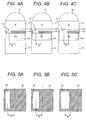
- FIGS. 4A to 4C are schematic cross-sectional views of an R pixel cell 50b, a G pixel cell 50b, and a B pixel cell 50b in the solid-state imaging element 5 illustrated in FIGS. 2 and 3 .
- FIG. 4A is a cross-sectional view of the R pixel cell 50b
- FIG. 4B is a cross-sectional view of the G pixel cell 50b
- FIG. 4C is a cross-sectional view of the B pixel cell 50b.
- the pixel cell 50a includes a semiconductor substrate 53 such as a silicon substrate, a photoelectric converting unit (PD) 54a provided in the semiconductor substrate 53, an insulating layer 56 formed on the photoelectric converting unit 54a, a color filter 57 formed on the insulating layer 56, and a micro lens 58 formed on the color filter 57.
- a semiconductor substrate 53 such as a silicon substrate
- PD photoelectric converting unit
- insulating layer 56 formed on the photoelectric converting unit 54a
- a color filter 57 formed on the insulating layer 56
- micro lens 58 formed on the color filter 57.
- a light shielding film 55 configured to limit a light incident range of the photoelectric converting unit 54a is formed in the insulating layer 56.
- An aperture 54 is formed at an upper side (a light entering side) of the photoelectric converting unit 54a in the light shielding film 55 and light condensed by the micro lens 58 is incident on the photoelectric converting unit 54a through the aperture 54.
- an optical axis of the micro lens 58 does not conform to a center of the aperture 54 and the center of the aperture 54 is off-centered to the left side in the row direction X with respect to the optical axis of the micro lens 58.
- the off-centered amount of the aperture 54 varies depending on the type of the pixel cell 50a.
- a relationship among an off-centered amount Or of the aperture 54 of the R pixel cell 50a, an off-centered amount Og of the aperture 54 of the G pixel cell 50a, and an off-centered amount Ob of the aperture 54 of the B pixel cell 50a is set to be Or > Og > Ob.
- the off-centered amount Or represents a distance between the position of the optical axis of the micro lens 58 in the R pixel cell 50a and the position of the center of the aperture 54, in the row direction X.
- the off-centered amount Og represents a distance between the position of the optical axis of the micro lens 58 in the G pixel cell 50a and the position of the center of the aperture 54, in the row direction X.
- the off-centered amount Ob represents a distance between the position of the optical axis of the micro lens 58 in the B pixel cell 50a and the position of the center of the aperture 54, in the row direction X.
- FIGS. 5A to 5C are plan views for each pixel cell 50a illustrated in FIGS. 4A to 4C , as viewed from the micro lens 58 side. In FIGS. 5A to 5C , the micro lens and the color filter are not illustrated.
- FIG. 5A illustrates a plan view of the R pixel cell 50a illustrated in FIG. 4A
- FIG. 5B illustrates a plan view of the G pixel cell 50a illustrated in FIG. 4B
- FIG. 5C illustrates a plan view of the B pixel cell 50a illustrated in FIG. 4C .
- the positions of left end portions of the apertures 54 of the light shielding films 55 are set to be the same in respective pixel cells 50a, and the positions of the right end portions in the row direction X are set such that the right end of a pixel cell 50a detecting light of a longer wavelength region is spaced farther away from the optical center of the pixel cell 50a (the position of the optical axis of the micro lens 58) the pixel cells 50a, thereby realizing the relationship of Or > Og> Ob.
- each pixel cell 50a may be provided with the pupil division performance.
- the phase difference AF may be precisely performed without causing variation in precision for obtaining phase difference information (a deviated amount of images which respectively correspond to a pair of luminous fluxes which pass through different pupil areas of the photographing optical system 1) depending on the types of the pixel cells 50a. Moreover, unnatural coloration does not occur in stereoscopic image data or two-dimensional captured image data so that the imaging quality can be enhanced.
- the sizes of the apertures K of the light shielding films 55 are changed depending on the detected wavelengths thereof, respectively.
- the sizes of the apertures K may be set to be the same in all the pixel cells 50.
- the pixel cells 50 may be configured such that the apertures 54 in all the pixel cells 50 have the same shape and the center positions of the apertures 54 vary depending on the types of the pixel cells 50.
- the apertures K have the same shape in all the pixel cells 50 as described above, manufacturing is facilitated, which results in cost reduction.
- phase difference AF precision or imaging quality may be improved only when at least a relationship of Or > Ob is satisfied since the difference between the sizes of the spot lights are most significant between the R pixel cells 50a and 50b and the B pixel cells 50a and 50b.
- FIG. 9 is a schematic plan view of a solid-state imaging element 5a which is a modified embodiment of the solid-state imaging element 5 illustrated in FIG. 2 .
- the solid-state imaging element 5a has a so-called honeycomb arrangement in which the pixel cells 50a and the pixel cells 50b of FIG. 2 are rotated by 45 degrees and odd-numbered pixel cell rows are shifted in the row direction X by 1/2 of the arrangement pitch of the pixel cells 50 in the row direction X.
- FIG. 10 is an enlarged view of a region H of the solid-state imaging element 5a illustrated in FIG. 9 .
- a separated distance from a center position of the aperture 54 of the light shielding film 55 in each pixel cell 50 which is an optical axis center of the each pixel cell 50 is as follows: R pixel cells 50a and 50b > G pixel cells 50a and 50b > B pixel cells 50a and 50b.
- FIG. 11 is a plan view illustrating a configuration of a solid-state imaging element 5b which is a modified embodiment of the solid-state imaging element 5 illustrated in FIG. 2 .
- the solid-state imaging elements 5 and 5a do not have a pixel cell which receives both of a pair of luminous fluxes which pass through different pupil regions of the photographing optical system 1 (a pixel cell in which a pupil is not divided).
- a solid-state imaging element 5b includes pixel cells 50c in which pupils are not divided, and the pixel cells 50a and 50b in which the pupils are divided as described above.
- some of the pixel cells 50c which are arranged two-dimensionally are formed as pixel cells 50a and 50b.
- some of the pixel cells 50c which detect R light component and some of the pixel cells 50c which detect G light component are substituted by the pixel cells 50a and 50b.
- the solid-state imaging element 5b includes, as pupil-divided pixels, only the pixel cells 50a and 50b which detect the R light component and the cells 50a and 50b which detect the G light component, the above-described relationship of Or and Og may be set to be Or > Og.
- the solid-state imaging element 5b includes, as the pupil-divided pixels, only the pixel cells 50a and 50b which detect the R light component and the pixel cells 50a and 50b which detect the B light component, the above-described relationship of Or and Ob may be set to be Or > Ob.
- the solid-state imaging element 5b includes, as the pupil-divided pixels, only the pixel cells 50a and 50b which detect the G light component and the pixel cells 50a and 50b which detect the B light component, the above-described relationship of Og and Ob may be set to be Og > Ob.
- the system control unit 11 performs the phase difference AF using signals obtained by the pixel cells 50a and 50b. Specifically, the system control unit 11 performs an AF control based on a phase difference between an image signal obtained by the pixel cells 50a and an image signal obtained by the pixel cells 50b.
- the solid-state imaging element 5b includes, as the pupil-divided pixels, the pixel cells 50a and 50b which detect the R light component, the pixel cells 50a and 50b which detect the G light component, and the pixel cells 50a and 50b which detect the B light component and when these three types of pixel cells 50a and 50b are arranged therein from end to end, it becomes possible to cope with both 3D photography and 2D photography.
- stereoscopic image data is generated using captured image signals obtained by the three types of the pixel cells 50a and 50b
- captured image data is generated using captured image signals obtained by the pixel cells 50c.
- the signals corresponding to the pixel cells 50a and 50b may be interpolated using the signals obtained by the pixel cells 50c.
- FIG. 12 is a plan view illustrating a configuration of a solid-state imaging element 5c which is a modified embodiment of the solid-state imaging element 5 illustrated in FIG. 2 .
- the solid-state imaging element 5c is the same as the solid-state imaging element 5 in that pixel cells 50a and pixel cells 50b are arranged two-dimensionally.
- the solid-state imaging element 5c has a configuration in which the pixel cells 50a are arranged in a Bayer pattern in odd numbered columns and, in relation to each pixel 50a, a pixel cell 50a which detects light having the same color as that detected by the pixel cell 50a is arranged next to the pixel cell 50a in the row direction X.
- pixel cell pairs are configured by the same types of pixel cells 50a and pixel cells 50b which are adjacent to each other in the row direction X.
- FIGS. 13A to 13C are views for illustrating in detail a pixel cell pair which detects an R light component, a pixel cell pair which detects a G light component, and a pixel cell pair which detects a B light component in the solid-state imaging element 5c illustrated in FIG. 12 .
- FIG. 13A illustrates a configuration of a pixel cell pair which detects an R light component in the solid-state imaging element 5c.
- FIG. 13B illustrates a configuration of a pixel cell pair which detects a G light component in the solid-state imaging element 5c.
- FIG. 13C illustrates a configuration of a pixel cell pair which detects a B light component in the solid-state imaging element 5c.
- one micro lens 53a is provided for a pixel cell pair.
- the micro lens 53a has an oval shape which is provided over two pixel cells 50 which configure a pixel cell pair.
- the distances between the optical axes of the micro lenses 53a and the centers of the apertures 54 of individual pixel cells 50 corresponding to the micro lenses 53a are set to be Or, Og, and Ob, respectively, and have the relationships as described above.
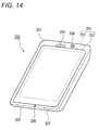
- FIG. 14 illustrates an outer appearance of a smart phone 200 which is an embodiment of the imaging apparatus of the present invention.
- the smart phone 200 illustrated in FIG. 14 includes a flat panel type case 201 and is provided, on one surface of the case 201, with a display input unit 204 in which a display panel 202 as a display unit and an operating panel 203 as an input unit are integrated.
- the case 201 includes a speaker 205, a microphone 206, an operating unit 207, and a camera 208.
- the configuration of the case 201 is not limited thereto. For example, a configuration in which the display unit and the input unit are independent from each other may be employed or a configuration having a folding structure or a slide mechanism may be employed.
- FIG. 15 is a block diagram illustrating a configuration of the smart phone 200 illustrated in FIG. 14 .
- the smart phone includes a wireless communication unit 210, a display input unit 204, a calling unit 211, an operating unit 207, a camera 208, a storage unit 212, an external input/output unit 213, a global positioning system (GPS) receiving unit 214, a motion sensor unit 215, a power supply 216, and a main control unit 220.
- the smart phone 200 is provided with a wireless communication function which performs mobile wireless communication through a base station device BS which is not illustrated and a mobile communication network NW which is also not illustrated.
- BS base station device
- NW mobile communication network
- the wireless communication unit 210 performs wireless communication with the base station device BS which is accommodated in the mobile communication network NW in accordance with an instruction of the main control unit 220. Using the wireless communication, the wireless communication unit 210 transmits/receives various file data such as voice data and image data, or electronic mail data, or receives web data, streaming data or the like.
- the display input unit 204 is provided with a display panel 202 and an operating panel 203 as a so-called touch panel which displays an image (a still image or a moving picture) or text information under the control of the main control unit 220 so as to visually transmit information to a user, and detects the user's operation on displayed information.
- the display panel 202 uses a liquid crystal display (LCD), an organic electro-luminescence display (OLED), or the like, as a display device.
- LCD liquid crystal display
- OLED organic electro-luminescence display
- the operating panel 203 is a device which is disposed to allow an image displayed on a display surface of the display panel 202 to be visually recognized and detects one or a plurality of coordinates which can be operated by the user's finger or a stylus.
- a detection signal generated based on the operation is output to the main control unit 220.
- the main control unit 220 detects an operating position (coordinate) on the display panel 202, based on the received detection signal.
- the display panel 202 and the operating panel 203 of the smart phone 200 exemplified as an embodiment of the imaging apparatus of the present invention are integrated with each other to constitute the display input unit 204, the operation panel 203 is disposed to completely cover the display panel 202.
- the operating panel 203 may be provided with a function of detecting the user's operation on a region other than the display panel 202.
- the operating panel 203 may include a detection region (hereinafter, referred to as a "display region”) on an overlapping portion which overlaps the display panel 202 and a detection region (hereinafter, referred to as a "non-display region”) on an outer peripheral portion which does not overlap the display panel 202.
- the operating panel 203 may include two sensitive regions of an outer peripheral portion and an inner portion other than the outer peripheral portion. A width of the outer peripheral portion is appropriately designed in accordance with the size of the case 201.
- a position detecting system employed in the operating panel 203 a matrix switch system, a resistive layer system, a surface elastic wave system, an infrared system, an electromagnetic induction system, or an electrostatic capacitive system may be exemplified, and any system may be employed.
- the calling unit 211 includes the speaker 205 and the microphone 206 in which the calling unit 211 converts the user's voice input through the microphone 206 into voice data to be processed by the main control unit 220 and outputs the converted voice data to the main control unit 220, or decodes voice data received by the wireless communication unit 210 or the external input/output unit 213 and outputs the decoded voice data from the speaker 205.
- the speaker 205 may be mounted on the same surface as the surface provided with the display input unit 204 and the microphone 206 may be mounted on a side surface of the case 201.
- the operating unit 207 is a hardware key which uses a key switch and receives an instruction from the user.
- the operating unit 207 is a push button type switch which is mounted on a side surface of the case 201 of the smart phone 200 and turned on when it is pressed by a finger and turned off by restoring force of a spring when the finger is removed.
- the storage unit 212 stores a control program or control data of the main control unit 220, application software, address data to which names, phone numbers, or the like of communication counterparts are correlated, transmitted/received electronic mail data, web data downloaded by web browsing or downloaded content data, and temporally stored streaming data.
- the storage unit 212 is configured by an internal storage unit 217 which is mounted in the smart phone and an external storage unit 218 which includes a detachable external memory slot.
- the internal storage unit 217 and the external storage unit 218 which configure the storage unit 212 may be implemented by using a storage medium such as a flash memory type, a hard disk type, a multimedia card micro type, a card type memory (e.g., MicroSD (registered trademark) memory), a random access memory (RAM), or a read only memory (ROM).
- a storage medium such as a flash memory type, a hard disk type, a multimedia card micro type, a card type memory (e.g., MicroSD (registered trademark) memory), a random access memory (RAM), or a read only memory (ROM).
- the external input/output unit 213 functions as an interface with all external devices connected to the smart phone 200 and are configured to be directly or indirectly connected to any other external device by communication (e.g., universal serial bus (USB) or IEEE1394) or a network (e.g., Internet, wireless LAN, Bluetooth (registered trademark), a radio frequency identification (RFID), an infrared data association (IrDA (registered trademark)), ultra wideband (UWD) (registered trademark), or a zigbee (registered trademark).
- a wired/wireless head set As external devices connected to the smart phone 200, a wired/wireless head set, a wired/wireless external charger, a wired/wireless data port, a memory card or a SIM (Subscriber Identity Module) card/UIM (User Identity Module) connected through a card socket, an external audio/video device connected through an audio/video input/output (I/O) terminal, a wirelessly connected external audio/video device, a wiredly/wirelessly connected smart phone, a wiredly/wirelessly connected personal computer, a wiredly/wirelessly connected PDA, a wiredly/wirelessly connected personal computer, or an earphone may be exemplified.
- the external input/output unit 213 transmits data received from such external devices to individual components in the smart phone 200 and may also allow the data in the smart phone 200 to be transmitted to an external device.
- the GPS receiving unit 214 receives a GPS signal transmitted from GPS satellites ST1 to STn according to an instruction from the main control unit 220 and performs a position measurement operation based on the received GPS signals to detect positional information including a latitude, a longitude, and a height of the smart phone 200.
- the GPS receiving unit 214 may obtain the positional information from the wireless communication unit 210 or the external input/output unit 213 (e.g., the wireless LAN), the GPS receiving unit 214 may also detect a position using that positional information.
- the motion sensor 215 includes, for example, a three-axis acceleration sensor and detects a physical movement of the smart phone 200 according to an instruction of the main control unit 220. When the physical movement of the smart phone 200 is detected, the movement direction or acceleration of the smart phone 200 is detected. The detected result is output to the main control unit 220.
- a power supply unit 216 supplies a power accumulated in a battery (not illustrated) to individual units of the smart phone 200 according to an instruction of the main control unit 220.
- the main control unit 220 includes a microprocessor and operates according to a control program or control data stored in the storage unit 212 and collectively controls individual units of the smart phone 200. Furthermore, the main control unit 220 is provided with a mobile communication control function and an application processing function to control individual units of a communication system in order to perform voice communication or data communication through the wireless communication unit 210.
- the application processing function is implemented when the main control unit 220 is operated according to the application software stored in the storage unit 212.
- the application processing function includes, for example, an infrared communication function which performs data communication with counterpart device by controlling the external input/output unit 213, an electronic mail function which transmits/receives an electronic mail, or a web browsing function which browses a web page.
- the main control unit 220 is provided with an image processing function which displays an image on the display input unit 204 based on the image data (still image or moving picture data) such as received data or downloaded streaming data.
- the image processing function refers to a function of decoding the image data and performing an image processing on the decoded result to display the image on the display input unit 204, by the main control unit 220.
- the main control unit 220 executes a display control of the display panel 202 and a operation detection control which detects the user's operation through the operating unit 207 and the operating panel 203.
- the main control unit 220 displays an icon to activate an application software or a software key such as a scroll bar (for making an instruction for continuous display in a connected state), or displays a window for preparing an electronic mail.
- the scroll bar refers to a software key for receiving an instruction to move a displayed portion of an image with respect to a large image which cannot enter into the display region of the display panel 202.
- the main control unit 220 detects the user's operation through the operating unit 207, receives the operation on the icon or an input of a character string on an input section of the window through the operating panel 203, or receives a scroll request of a displayed image through the scroll bar.
- the main control unit 220 determines whether the operating position of the operating panel 203 is an overlapping portion (display region) which overlaps with the display panel 202 or an outer peripheral portion (non-display region) which does not overlap with the display panel 202 other than the overlapping portion, and is provided with a touch panel control function that controls a sensitive region of the operating panel 203 or a display position of the software key.
- the main control unit 220 detects a gesture operation with respect to the operating panel 203 and executes a predetermined function according to the detected the gesture operation.
- the gesture operation refers to an operation which draws a trace using a finger, designates a plurality of positions simultaneously, or a combination thereof to draw a trace for at least one of the plurality of positions, rather than a simple touch operation of the related art.
- the camera 208 includes a configuration other than the external memory control unit 20, the recording medium 21, the display control unit 22, the display unit 23, and the operating unit 14 in the digital camera illustrated in FIG. 1 . Captured image data generated by the camera 208 may be stored in the storage unit 212, or output through the external input/output unit 213 or the wireless communication unit 210. As illustrated in FIG. 14 , although the camera 208 is mounted on the same surface as the display input unit 204 in the smart phone 200, the mounting position of the camera 208 is not limited thereto and the camera 208 may be mounted on a rear surface of the display input unit 204.
- the camera 208 may be used for various functions of the smart phone 200.
- an image obtained by the camera 208 may be displayed on the display panel 202
- the image of the camera 208 may be used as one of operation inputs of the operating panel 203.
- the GPS receiving unit 214 detects the position
- the position may be detected with reference to the image from the camera 208.
- an optical axis direction of the camera 208 of the smart phone 200 may be determined with reference to the image from the camera 208, either without using the 3-axis acceleration sensor or using the 3-axis acceleration sensor, a current usage environment may also be determined.
- the image from the camera 208 can be used in the application software.
- positional information obtained by the GPS receiving unit 214, voice information obtained by the microphone 206 (which may be text information obtained by performing a voice-text conversion by the main control unit or the like), or posture information obtained by the motion sensor 215 may be added to the image data or a still image or a moving picture to be stored in the storage unit 212 or may be be output through the external input/output unit 213 or the wireless communication unit 210.
- an imaging element capable of outputting a pair of image signals which correspond to a pair of luminous fluxes which pass through different pupil areas of a photographing optical system, respectively, the imaging element including: pixel cells including photoelectric converting units, micro lenses provided at light entrance sides of the photoelectric converting units to condense lights onto the photoelectric converting units and light shielding films which is provided between the photoelectric converting units and the micro lenses and has apertures at the light entrance sides of the photoelectric converting units, in which the pixel cells include plural sets of pairs each having a first pixel cell and a second pixel cell, center positions of apertures of light shielding films of the first pixel cell and the second pixel cell being off-centered in opposite directions with respect to an optical axis of the micro lens, the first pixel cell and the second pixel cell are divided into plural types which detect lights of different wavelength bands, respectively, and among the pixel cells, a distance from an optical axis of the micro lens to the center of the aperture of the micro lens for each of the first pixel cell and
- the imaging element in which the plural types of pixel cells include at least two types of a pixel cell which detects a red light component, a pixel cell which detects a blue light component and a pixel cell which detects a green light component.
- the imaging element in which the imaging element is set to be (the distance in the pixel cell which detects the red light component) > (the distance in the pixel cell which detects the green light component) > (the distance in the pixel cell which detects the blue light component).
- the imaging element in which the distances for two of the pixel cell which detects the red light component, the pixel cell which detects the blue light component and the pixel cell which detects the green light component are set to be the same.
- the imaging element in which the distances for the pixel cell which detects the red light component and the pixel cell which detects the green light component are set to be the same, and the distance for the pixel cell which detects the blue light component is set to be shorter than the distances for the pixel cell which detects the red light component and the pixel cell which detects the green light component.
- the imaging element in which the distances for the pixel cell which detects the blue light component and the pixel cell which detects the green light component are set to be the same, and the distance for the pixel cell which detects the red light component is set to be longer than the distances for the pixel cell which detects the blue light component and the pixel cell which detects the green light component.
- the imaging element in which the apertures of the light shielding films in at least four pixel cells have the same shape.
- each of the pairs is configured by the first pixel cell and the second pixel cell which is disposed to be adjacent to the first pixel cell and detects light in the same wavelength band as the first pixel cell, and the pairs are arranged two-dimensionally.
- an imaging apparatus including the imaging element.
- the imaging apparatus further including: a stereoscopic image generating unit which generates stereoscopic image data using signals obtained from the plural sets of pairs.
- the imaging apparatus further including: a focus adjusting unit which adjusts a focus using signals which is obtained from the plural sets of pairs.
- the imaging element and the imaging apparatus according to the present invention precisely detect a deviated amount of images which respectively correspond to a pair of luminous fluxes which have passed through different pupil areas of an photographing optical system such that precision of the phase difference AF may be improved and unnatural coloration on the captured image may be prevented, thereby improving an imaging quality. Therefore, the imaging element and the imaging apparatus may be usefully used for various information devices such as a digital camera and a smart phone.
Landscapes
- Engineering & Computer Science (AREA)
- Multimedia (AREA)
- Signal Processing (AREA)
- Physics & Mathematics (AREA)
- Spectroscopy & Molecular Physics (AREA)
- Solid State Image Pick-Up Elements (AREA)
- Studio Devices (AREA)
- Transforming Light Signals Into Electric Signals (AREA)
- Automatic Focus Adjustment (AREA)
- Stereoscopic And Panoramic Photography (AREA)
- Focusing (AREA)
Claims (11)
- Abbildungselement, das in der Lage ist, ein Paar Bildsignale auszugeben, die einem Paar Lichtströme entsprechen, die jeweils verschiedene Pupillenbereiche eines optischen Fotografiesystems durchqueren, wobei das Abbildungselement Folgendes umfasst:Pixelzellen (50), die fotoelektrische Umwandlungseinheiten, Mikrolinsen (58), die an Lichteintrittsseiten der fotoelektrischen Umwandlungseinheiten bereitgestellt sind, um Lichter auf die fotoelektrischen Umwandlungseinheiten zu kondensieren, und dünne Lichtabschirmungsschichten (55) umfassen, die zwischen den fotoelektrischen Umwandlungseinheiten und den Mikrolinsen bereitgestellt sind und Aperturen (54) an den Lichteintrittsseiten der fotoelektrischen Umwandlungseinheiten aufweisen, wobei die Pixelzellen mehrere Mengen von Paaren umfassen, die jeweils eine erste Pixelzelle und eine zweite Pixelzelle aufweisen, wobei mittlere Positionen von Aperturen von dünnen Lichtabschirmungsschichten der ersten Pixelzelle und der zweiten Pixelzelle in entgegengesetzten Richtungen in Bezug zu einer optischen Achse der Mikrolinse außermittig sind,die erste Pixelzelle und die zweite Pixelzelle in mehrere Typen unterteilt sind, die jeweils Lichter mit verschiedenen Wellenlängenbändern ermitteln, unddadurch gekennzeichnet, dass unter den Pixelzellen ein außermittiger Betrag der (Or, Og, Ob) optischen Achse der Mikrolinse zur Mitte der Apertur der dünnen Lichtabschirmungsschicht für jede von der ersten Pixelzelle und der zweiten Pixelzelle, in der ein Wellenlängenband des durch die fotoelektrische Umwandlungseinheit ermittelten Lichts die längste Wellenlängenregion wird, länger ist als der außermittige Betrag für jede von der ersten Pixelzelle und der zweiten Pixelzelle, in der ein Wellenlängenband des Lichts die kürzeste Wellenlängenregion wird (Or>Og>Ob).
- Abbildungselement nach Anspruch 1, wobei die mehreren Typen von Pixelzellen mindestens zwei Typen von einer Pixelzelle, die eine Rotlichtkomponente ermittelt, einer Pixelzelle, die eine Blaulichtkomponente ermittelt, und einer Pixelzelle umfassen, die eine Grünlichtkomponente ermittelt.
- Abbildungselement nach Anspruch 2, wobei das Abbildungselement eingestellt ist, um Folgendes zu sein: (der Abstand in der Pixelzelle, die die Rotlichtkomponente ermittelt) > (der Abstand in der Pixelzelle, die die Grünlichtkomponente ermittelt) > (der Abstand in der Pixelzelle, die die Blaulichtkomponente ermittelt).
- Abbildungselement nach Anspruch 2, wobei die Abstände von zwei von der Pixelzelle, die die Rotlichtkomponente ermittelt, der Pixelzelle, die die Blaulichtkomponente ermittelt, und der Pixelzelle, die die Grünlichtkomponente ermittelt, eingestellt sind, um gleich zu sein.
- Abbildungselement nach Anspruch 4, wobei die Abstände für die Pixelzelle, die die Rotlichtkomponente ermittelt, und die Pixelzelle, die die Grünlichtkomponente ermittelt, eingestellt sind, um gleich zu sein, und der Abstand für die Pixelzelle, die die Blaulichtkomponente ermittelt, eingestellt ist, um kürzer zu sein als die Abstände für die Pixelzelle, die die Rotlichtkomponente ermittelt, und die Pixelzelle, die die Grünlichtkomponente ermittelt.
- Abbildungselement nach Anspruch 4, wobei die Abstände für die Pixelzelle, die die Blaulichtkomponente ermittelt, und die Pixelzelle, die die Grünlichtkomponente ermittelt, eingestellt sind, um gleich zu sein, und der Abstand für die Pixelzelle, die die Rotlichtkomponente ermittelt, eingestellt ist, um länger zu sein, als die Abstände für die Pixelzelle, die die Blaulichtkomponente ermittelt, und die Pixelzelle, die die Grünlichtkomponente ermittelt.
- Abbildungselement nach einem der Ansprüche 1 bis 6, wobei die Aperturen der dünnen Lichtabschirmungsschichten in mindestens vier Pixelzellen die gleiche Form aufweisen.
- Abbildungselement nach einem der Ansprüche 1 bis 6, wobei jedes von den Paaren durch die erste Pixelzelle und die zweite Pixelzelle ausgestaltet ist, die angeordnet ist, um der ersten Pixelzelle benachbart zu sein, und Licht in dem gleichen Wellenlängenband ermittelt wie die erste Pixelzelle und die Paare zweidimensional angeordnet sind.
- Abbildungsvorrichtung, die Folgendes umfasst:das Abbildungselement nach einem der Ansprüche 1 bis 8.
- Abbildungsvorrichtung nach Anspruch 9, die ferner Folgendes umfasst:eine Einheit zur Erzeugung eines stereoskopischen Bildes, das unter Verwendung von Signalen, die von den mehreren Mengen von Paaren erhalten werden, stereoskopische Bilddaten erzeugt.
- Abbildungsvorrichtung nach Anspruch 9 oder 10, die ferner Folgendes umfasst:eine Fokusanpassungseinheit, die einen Fokus unter Verwendung von Signalen anpasst, die von den mehreren Mengen von Paaren erhalten werden.
Applications Claiming Priority (2)
| Application Number | Priority Date | Filing Date | Title |
|---|---|---|---|
| JP2012074309 | 2012-03-28 | ||
| PCT/JP2013/051283 WO2013145821A1 (ja) | 2012-03-28 | 2013-01-23 | 撮像素子及び撮像装置 |
Publications (3)
| Publication Number | Publication Date |
|---|---|
| EP2833406A1 EP2833406A1 (de) | 2015-02-04 |
| EP2833406A4 EP2833406A4 (de) | 2015-10-28 |
| EP2833406B1 true EP2833406B1 (de) | 2016-10-26 |
Family
ID=49259107
Family Applications (1)
| Application Number | Title | Priority Date | Filing Date |
|---|---|---|---|
| EP13769765.2A Not-in-force EP2833406B1 (de) | 2012-03-28 | 2013-01-23 | Abbildungselement und abbildungsvorrichtung |
Country Status (5)
| Country | Link |
|---|---|
| US (1) | US9204114B2 (de) |
| EP (1) | EP2833406B1 (de) |
| JP (1) | JP5542248B2 (de) |
| CN (1) | CN104221149B (de) |
| WO (1) | WO2013145821A1 (de) |
Families Citing this family (6)
| Publication number | Priority date | Publication date | Assignee | Title |
|---|---|---|---|---|
| CN106200882B (zh) * | 2015-04-30 | 2019-05-10 | 原相科技股份有限公司 | 感测元件及光学测距系统 |
| CN110598685B (zh) * | 2015-09-14 | 2023-06-30 | 原相科技股份有限公司 | 分辨前景的成像装置 |
| JP2017157804A (ja) * | 2016-03-04 | 2017-09-07 | キヤノン株式会社 | 撮像装置 |
| DE102016212778A1 (de) * | 2016-07-13 | 2018-01-18 | Robert Bosch Gmbh | Bildsensor für eine Kamera |
| US10270947B2 (en) * | 2016-09-15 | 2019-04-23 | Microsoft Technology Licensing, Llc | Flat digital image sensor |
| KR102693484B1 (ko) * | 2016-09-23 | 2024-08-09 | 삼성전자주식회사 | 입사광의 파장 스펙트럼을 검출하는 방법 및 이를 수행하는 전자 장치 |
Family Cites Families (15)
| Publication number | Priority date | Publication date | Assignee | Title |
|---|---|---|---|---|
| JP2005086186A (ja) * | 2003-09-11 | 2005-03-31 | Matsushita Electric Ind Co Ltd | 固体撮像装置とその製造方法 |
| US7274011B2 (en) * | 2004-12-27 | 2007-09-25 | Teledyne Licensing, Llc | Spectral imager and fabrication method |
| JP4915126B2 (ja) * | 2006-04-10 | 2012-04-11 | 株式会社ニコン | 固体撮像装置、および電子カメラ |
| DE102006047941B4 (de) * | 2006-10-10 | 2008-10-23 | Fraunhofer-Gesellschaft zur Förderung der angewandten Forschung e.V. | Vorrichtung zur Homogenisierung von Strahlung mit nicht regelmäßigen Mikrolinsenarrays |
| KR100825805B1 (ko) * | 2007-02-13 | 2008-04-29 | 삼성전자주식회사 | 이미지 센서 소자 및 그 센서 소자의 제조방법 |
| US7898738B2 (en) * | 2007-09-10 | 2011-03-01 | Oki Data Corporation | Lens array, manufacturing method thereof, LED head having lens array, exposure device having LED head, image forming apparatus having exposure device, and reading apparatus |
| JP5029268B2 (ja) * | 2007-10-01 | 2012-09-19 | 株式会社ニコン | 電子カメラ |
| WO2009087974A1 (ja) * | 2008-01-11 | 2009-07-16 | Panasonic Corporation | 複眼カメラモジュール |
| US8748799B2 (en) * | 2010-12-14 | 2014-06-10 | Zena Technologies, Inc. | Full color single pixel including doublet or quadruplet si nanowires for image sensors |
| JP2010093081A (ja) * | 2008-10-08 | 2010-04-22 | Panasonic Corp | 固体撮像装置およびその製造方法 |
| JP5311960B2 (ja) * | 2008-10-10 | 2013-10-09 | キヤノン株式会社 | 撮像装置、その制御方法及びプログラム |
| US8558940B2 (en) * | 2008-11-27 | 2013-10-15 | Nikon Corporation | Image sensor and image-capturing device |
| JP5278123B2 (ja) | 2009-04-06 | 2013-09-04 | 株式会社ニコン | 撮像装置 |
| JP5159700B2 (ja) * | 2009-05-19 | 2013-03-06 | キヤノン株式会社 | 光学装置及び焦点検出方法 |
| JPWO2011148574A1 (ja) * | 2010-05-28 | 2013-07-25 | パナソニック株式会社 | 固体撮像装置 |
-
2013
- 2013-01-23 EP EP13769765.2A patent/EP2833406B1/de not_active Not-in-force
- 2013-01-23 JP JP2014507464A patent/JP5542248B2/ja not_active Expired - Fee Related
- 2013-01-23 WO PCT/JP2013/051283 patent/WO2013145821A1/ja not_active Ceased
- 2013-01-23 CN CN201380017557.XA patent/CN104221149B/zh active Active
-
2014
- 2014-09-26 US US14/498,558 patent/US9204114B2/en active Active
Also Published As
| Publication number | Publication date |
|---|---|
| EP2833406A4 (de) | 2015-10-28 |
| US20150009373A1 (en) | 2015-01-08 |
| CN104221149B (zh) | 2016-08-24 |
| US9204114B2 (en) | 2015-12-01 |
| CN104221149A (zh) | 2014-12-17 |
| WO2013145821A1 (ja) | 2013-10-03 |
| JP5542248B2 (ja) | 2014-07-09 |
| EP2833406A1 (de) | 2015-02-04 |
| JPWO2013145821A1 (ja) | 2015-12-10 |
Similar Documents
| Publication | Publication Date | Title |
|---|---|---|
| US10003731B2 (en) | Image element, and imaging device and imaging method using the same for achieving improved image quality regardless of an incident angle of light | |
| US9386216B2 (en) | Imaging device, defocus amount calculating method, and imaging optical system | |
| US9288384B2 (en) | Image device and focus control method | |
| US9386285B2 (en) | Imaging element and imaging device with microlenses and color pixels | |
| EP3086546B1 (de) | Bilderfassungsmodul und bilderfassungsvorrichtung | |
| CN110447223B (zh) | 摄像装置 | |
| JP6165680B2 (ja) | 撮像装置 | |
| CN104813648B (zh) | 图像处理装置、摄像装置、及图像处理方法 | |
| JP5799178B2 (ja) | 撮像装置及び合焦制御方法 | |
| EP2961153B1 (de) | Bildaufnahmevorrichtung | |
| US9432569B2 (en) | Imaging device and focus control method | |
| US9204114B2 (en) | Imaging element and imaging apparatus | |
| US9344646B2 (en) | Imaging device and imaging method | |
| JP5740053B2 (ja) | 撮像装置及び画像処理方法 | |
| JP5740053B6 (ja) | 撮像装置及び画像処理方法 |
Legal Events
| Date | Code | Title | Description |
|---|---|---|---|
| PUAI | Public reference made under article 153(3) epc to a published international application that has entered the european phase |
Free format text: ORIGINAL CODE: 0009012 |
|
| 17P | Request for examination filed |
Effective date: 20140926 |
|
| AK | Designated contracting states |
Kind code of ref document: A1 Designated state(s): AL AT BE BG CH CY CZ DE DK EE ES FI FR GB GR HR HU IE IS IT LI LT LU LV MC MK MT NL NO PL PT RO RS SE SI SK SM TR |
|
| AX | Request for extension of the european patent |
Extension state: BA ME |
|
| DAX | Request for extension of the european patent (deleted) | ||
| REG | Reference to a national code |
Ref country code: DE Ref legal event code: R079 Ref document number: 602013013282 Country of ref document: DE Free format text: PREVIOUS MAIN CLASS: H01L0027140000 Ipc: H01L0027146000 |
|
| RA4 | Supplementary search report drawn up and despatched (corrected) |
Effective date: 20150930 |
|
| RIC1 | Information provided on ipc code assigned before grant |
Ipc: H04N 5/369 20110101ALI20150924BHEP Ipc: H04N 9/04 20060101ALI20150924BHEP Ipc: H04N 5/232 20060101ALI20150924BHEP Ipc: H01L 27/146 20060101AFI20150924BHEP Ipc: H04N 101/00 20060101ALI20150924BHEP |
|
| GRAP | Despatch of communication of intention to grant a patent |
Free format text: ORIGINAL CODE: EPIDOSNIGR1 |
|
| INTG | Intention to grant announced |
Effective date: 20160518 |
|
| GRAS | Grant fee paid |
Free format text: ORIGINAL CODE: EPIDOSNIGR3 |
|
| GRAA | (expected) grant |
Free format text: ORIGINAL CODE: 0009210 |
|
| AK | Designated contracting states |
Kind code of ref document: B1 Designated state(s): AL AT BE BG CH CY CZ DE DK EE ES FI FR GB GR HR HU IE IS IT LI LT LU LV MC MK MT NL NO PL PT RO RS SE SI SK SM TR |
|
| REG | Reference to a national code |
Ref country code: GB Ref legal event code: FG4D |
|
| REG | Reference to a national code |
Ref country code: CH Ref legal event code: EP |
|
| REG | Reference to a national code |
Ref country code: AT Ref legal event code: REF Ref document number: 840563 Country of ref document: AT Kind code of ref document: T Effective date: 20161115 |
|
| REG | Reference to a national code |
Ref country code: IE Ref legal event code: FG4D |
|
| REG | Reference to a national code |
Ref country code: DE Ref legal event code: R096 Ref document number: 602013013282 Country of ref document: DE |
|
| REG | Reference to a national code |
Ref country code: LT Ref legal event code: MG4D |
|
| PG25 | Lapsed in a contracting state [announced via postgrant information from national office to epo] |
Ref country code: LV Free format text: LAPSE BECAUSE OF FAILURE TO SUBMIT A TRANSLATION OF THE DESCRIPTION OR TO PAY THE FEE WITHIN THE PRESCRIBED TIME-LIMIT Effective date: 20161026 |
|
| REG | Reference to a national code |
Ref country code: NL Ref legal event code: MP Effective date: 20161026 |
|
| REG | Reference to a national code |
Ref country code: AT Ref legal event code: MK05 Ref document number: 840563 Country of ref document: AT Kind code of ref document: T Effective date: 20161026 |
|
| PG25 | Lapsed in a contracting state [announced via postgrant information from national office to epo] |
Ref country code: LT Free format text: LAPSE BECAUSE OF FAILURE TO SUBMIT A TRANSLATION OF THE DESCRIPTION OR TO PAY THE FEE WITHIN THE PRESCRIBED TIME-LIMIT Effective date: 20161026 Ref country code: GR Free format text: LAPSE BECAUSE OF FAILURE TO SUBMIT A TRANSLATION OF THE DESCRIPTION OR TO PAY THE FEE WITHIN THE PRESCRIBED TIME-LIMIT Effective date: 20170127 Ref country code: NO Free format text: LAPSE BECAUSE OF FAILURE TO SUBMIT A TRANSLATION OF THE DESCRIPTION OR TO PAY THE FEE WITHIN THE PRESCRIBED TIME-LIMIT Effective date: 20170126 Ref country code: SE Free format text: LAPSE BECAUSE OF FAILURE TO SUBMIT A TRANSLATION OF THE DESCRIPTION OR TO PAY THE FEE WITHIN THE PRESCRIBED TIME-LIMIT Effective date: 20161026 |
|
| PG25 | Lapsed in a contracting state [announced via postgrant information from national office to epo] |
Ref country code: ES Free format text: LAPSE BECAUSE OF FAILURE TO SUBMIT A TRANSLATION OF THE DESCRIPTION OR TO PAY THE FEE WITHIN THE PRESCRIBED TIME-LIMIT Effective date: 20161026 Ref country code: FI Free format text: LAPSE BECAUSE OF FAILURE TO SUBMIT A TRANSLATION OF THE DESCRIPTION OR TO PAY THE FEE WITHIN THE PRESCRIBED TIME-LIMIT Effective date: 20161026 Ref country code: IS Free format text: LAPSE BECAUSE OF FAILURE TO SUBMIT A TRANSLATION OF THE DESCRIPTION OR TO PAY THE FEE WITHIN THE PRESCRIBED TIME-LIMIT Effective date: 20170226 Ref country code: BE Free format text: LAPSE BECAUSE OF FAILURE TO SUBMIT A TRANSLATION OF THE DESCRIPTION OR TO PAY THE FEE WITHIN THE PRESCRIBED TIME-LIMIT Effective date: 20161026 Ref country code: HR Free format text: LAPSE BECAUSE OF FAILURE TO SUBMIT A TRANSLATION OF THE DESCRIPTION OR TO PAY THE FEE WITHIN THE PRESCRIBED TIME-LIMIT Effective date: 20161026 Ref country code: RS Free format text: LAPSE BECAUSE OF FAILURE TO SUBMIT A TRANSLATION OF THE DESCRIPTION OR TO PAY THE FEE WITHIN THE PRESCRIBED TIME-LIMIT Effective date: 20161026 Ref country code: PT Free format text: LAPSE BECAUSE OF FAILURE TO SUBMIT A TRANSLATION OF THE DESCRIPTION OR TO PAY THE FEE WITHIN THE PRESCRIBED TIME-LIMIT Effective date: 20170227 Ref country code: AT Free format text: LAPSE BECAUSE OF FAILURE TO SUBMIT A TRANSLATION OF THE DESCRIPTION OR TO PAY THE FEE WITHIN THE PRESCRIBED TIME-LIMIT Effective date: 20161026 Ref country code: NL Free format text: LAPSE BECAUSE OF FAILURE TO SUBMIT A TRANSLATION OF THE DESCRIPTION OR TO PAY THE FEE WITHIN THE PRESCRIBED TIME-LIMIT Effective date: 20161026 Ref country code: PL Free format text: LAPSE BECAUSE OF FAILURE TO SUBMIT A TRANSLATION OF THE DESCRIPTION OR TO PAY THE FEE WITHIN THE PRESCRIBED TIME-LIMIT Effective date: 20161026 |
|
| REG | Reference to a national code |
Ref country code: DE Ref legal event code: R097 Ref document number: 602013013282 Country of ref document: DE |
|
| PG25 | Lapsed in a contracting state [announced via postgrant information from national office to epo] |
Ref country code: RO Free format text: LAPSE BECAUSE OF FAILURE TO SUBMIT A TRANSLATION OF THE DESCRIPTION OR TO PAY THE FEE WITHIN THE PRESCRIBED TIME-LIMIT Effective date: 20161026 Ref country code: SK Free format text: LAPSE BECAUSE OF FAILURE TO SUBMIT A TRANSLATION OF THE DESCRIPTION OR TO PAY THE FEE WITHIN THE PRESCRIBED TIME-LIMIT Effective date: 20161026 Ref country code: DK Free format text: LAPSE BECAUSE OF FAILURE TO SUBMIT A TRANSLATION OF THE DESCRIPTION OR TO PAY THE FEE WITHIN THE PRESCRIBED TIME-LIMIT Effective date: 20161026 Ref country code: EE Free format text: LAPSE BECAUSE OF FAILURE TO SUBMIT A TRANSLATION OF THE DESCRIPTION OR TO PAY THE FEE WITHIN THE PRESCRIBED TIME-LIMIT Effective date: 20161026 Ref country code: CZ Free format text: LAPSE BECAUSE OF FAILURE TO SUBMIT A TRANSLATION OF THE DESCRIPTION OR TO PAY THE FEE WITHIN THE PRESCRIBED TIME-LIMIT Effective date: 20161026 |
|
| PG25 | Lapsed in a contracting state [announced via postgrant information from national office to epo] |
Ref country code: IT Free format text: LAPSE BECAUSE OF FAILURE TO SUBMIT A TRANSLATION OF THE DESCRIPTION OR TO PAY THE FEE WITHIN THE PRESCRIBED TIME-LIMIT Effective date: 20161026 Ref country code: BG Free format text: LAPSE BECAUSE OF FAILURE TO SUBMIT A TRANSLATION OF THE DESCRIPTION OR TO PAY THE FEE WITHIN THE PRESCRIBED TIME-LIMIT Effective date: 20170126 Ref country code: SM Free format text: LAPSE BECAUSE OF FAILURE TO SUBMIT A TRANSLATION OF THE DESCRIPTION OR TO PAY THE FEE WITHIN THE PRESCRIBED TIME-LIMIT Effective date: 20161026 |
|
| REG | Reference to a national code |
Ref country code: CH Ref legal event code: PL |
|
| PLBE | No opposition filed within time limit |
Free format text: ORIGINAL CODE: 0009261 |
|
| STAA | Information on the status of an ep patent application or granted ep patent |
Free format text: STATUS: NO OPPOSITION FILED WITHIN TIME LIMIT |
|
| GBPC | Gb: european patent ceased through non-payment of renewal fee |
Effective date: 20170126 |
|
| PG25 | Lapsed in a contracting state [announced via postgrant information from national office to epo] |
Ref country code: MC Free format text: LAPSE BECAUSE OF FAILURE TO SUBMIT A TRANSLATION OF THE DESCRIPTION OR TO PAY THE FEE WITHIN THE PRESCRIBED TIME-LIMIT Effective date: 20161026 |
|
| 26N | No opposition filed |
Effective date: 20170727 |
|
| REG | Reference to a national code |
Ref country code: FR Ref legal event code: ST Effective date: 20170929 |
|
| PG25 | Lapsed in a contracting state [announced via postgrant information from national office to epo] |
Ref country code: CH Free format text: LAPSE BECAUSE OF NON-PAYMENT OF DUE FEES Effective date: 20170131 Ref country code: FR Free format text: LAPSE BECAUSE OF NON-PAYMENT OF DUE FEES Effective date: 20170131 Ref country code: LI Free format text: LAPSE BECAUSE OF NON-PAYMENT OF DUE FEES Effective date: 20170131 |
|
| REG | Reference to a national code |
Ref country code: IE Ref legal event code: MM4A |
|
| PG25 | Lapsed in a contracting state [announced via postgrant information from national office to epo] |
Ref country code: SI Free format text: LAPSE BECAUSE OF FAILURE TO SUBMIT A TRANSLATION OF THE DESCRIPTION OR TO PAY THE FEE WITHIN THE PRESCRIBED TIME-LIMIT Effective date: 20161026 Ref country code: GB Free format text: LAPSE BECAUSE OF NON-PAYMENT OF DUE FEES Effective date: 20170126 Ref country code: LU Free format text: LAPSE BECAUSE OF NON-PAYMENT OF DUE FEES Effective date: 20170123 |
|
| PG25 | Lapsed in a contracting state [announced via postgrant information from national office to epo] |
Ref country code: IE Free format text: LAPSE BECAUSE OF NON-PAYMENT OF DUE FEES Effective date: 20170123 |
|
| PG25 | Lapsed in a contracting state [announced via postgrant information from national office to epo] |
Ref country code: MT Free format text: LAPSE BECAUSE OF NON-PAYMENT OF DUE FEES Effective date: 20170123 |
|
| PG25 | Lapsed in a contracting state [announced via postgrant information from national office to epo] |
Ref country code: HU Free format text: LAPSE BECAUSE OF FAILURE TO SUBMIT A TRANSLATION OF THE DESCRIPTION OR TO PAY THE FEE WITHIN THE PRESCRIBED TIME-LIMIT; INVALID AB INITIO Effective date: 20130123 |
|
| PG25 | Lapsed in a contracting state [announced via postgrant information from national office to epo] |
Ref country code: CY Free format text: LAPSE BECAUSE OF FAILURE TO SUBMIT A TRANSLATION OF THE DESCRIPTION OR TO PAY THE FEE WITHIN THE PRESCRIBED TIME-LIMIT Effective date: 20161026 |
|
| PG25 | Lapsed in a contracting state [announced via postgrant information from national office to epo] |
Ref country code: MK Free format text: LAPSE BECAUSE OF FAILURE TO SUBMIT A TRANSLATION OF THE DESCRIPTION OR TO PAY THE FEE WITHIN THE PRESCRIBED TIME-LIMIT Effective date: 20161026 |
|
| PG25 | Lapsed in a contracting state [announced via postgrant information from national office to epo] |
Ref country code: TR Free format text: LAPSE BECAUSE OF FAILURE TO SUBMIT A TRANSLATION OF THE DESCRIPTION OR TO PAY THE FEE WITHIN THE PRESCRIBED TIME-LIMIT Effective date: 20161026 |
|
| PGFP | Annual fee paid to national office [announced via postgrant information from national office to epo] |
Ref country code: DE Payment date: 20200107 Year of fee payment: 8 |
|
| PG25 | Lapsed in a contracting state [announced via postgrant information from national office to epo] |
Ref country code: AL Free format text: LAPSE BECAUSE OF FAILURE TO SUBMIT A TRANSLATION OF THE DESCRIPTION OR TO PAY THE FEE WITHIN THE PRESCRIBED TIME-LIMIT Effective date: 20161026 |
|
| REG | Reference to a national code |
Ref country code: DE Ref legal event code: R119 Ref document number: 602013013282 Country of ref document: DE |
|
| PG25 | Lapsed in a contracting state [announced via postgrant information from national office to epo] |
Ref country code: DE Free format text: LAPSE BECAUSE OF NON-PAYMENT OF DUE FEES Effective date: 20210803 |