EP2833409A1 - Transistor à effet de champ en carbure de silicium - Google Patents
Transistor à effet de champ en carbure de silicium Download PDFInfo
- Publication number
- EP2833409A1 EP2833409A1 EP12873344.1A EP12873344A EP2833409A1 EP 2833409 A1 EP2833409 A1 EP 2833409A1 EP 12873344 A EP12873344 A EP 12873344A EP 2833409 A1 EP2833409 A1 EP 2833409A1
- Authority
- EP
- European Patent Office
- Prior art keywords
- film
- silicon carbide
- layer
- field effect
- sic
- Prior art date
- Legal status (The legal status is an assumption and is not a legal conclusion. Google has not performed a legal analysis and makes no representation as to the accuracy of the status listed.)
- Withdrawn
Links
Images




Classifications
-
- H—ELECTRICITY
- H10—SEMICONDUCTOR DEVICES; ELECTRIC SOLID-STATE DEVICES NOT OTHERWISE PROVIDED FOR
- H10D—INORGANIC ELECTRIC SEMICONDUCTOR DEVICES
- H10D12/00—Bipolar devices controlled by the field effect, e.g. insulated-gate bipolar transistors [IGBT]
- H10D12/01—Manufacture or treatment
- H10D12/031—Manufacture or treatment of IGBTs
-
- H—ELECTRICITY
- H10—SEMICONDUCTOR DEVICES; ELECTRIC SOLID-STATE DEVICES NOT OTHERWISE PROVIDED FOR
- H10D—INORGANIC ELECTRIC SEMICONDUCTOR DEVICES
- H10D30/00—Field-effect transistors [FET]
- H10D30/60—Insulated-gate field-effect transistors [IGFET]
- H10D30/63—Vertical IGFETs
- H10D30/635—Vertical IGFETs having no inversion channels, e.g. vertical accumulation channel FETs [ACCUFET] or normally-on vertical IGFETs
-
- H—ELECTRICITY
- H10—SEMICONDUCTOR DEVICES; ELECTRIC SOLID-STATE DEVICES NOT OTHERWISE PROVIDED FOR
- H10D—INORGANIC ELECTRIC SEMICONDUCTOR DEVICES
- H10D30/00—Field-effect transistors [FET]
- H10D30/60—Insulated-gate field-effect transistors [IGFET]
- H10D30/64—Double-diffused metal-oxide semiconductor [DMOS] FETs
- H10D30/66—Vertical DMOS [VDMOS] FETs
-
- H—ELECTRICITY
- H10—SEMICONDUCTOR DEVICES; ELECTRIC SOLID-STATE DEVICES NOT OTHERWISE PROVIDED FOR
- H10D—INORGANIC ELECTRIC SEMICONDUCTOR DEVICES
- H10D30/00—Field-effect transistors [FET]
- H10D30/60—Insulated-gate field-effect transistors [IGFET]
- H10D30/69—IGFETs having charge trapping gate insulators, e.g. MNOS transistors
-
- H—ELECTRICITY
- H10—SEMICONDUCTOR DEVICES; ELECTRIC SOLID-STATE DEVICES NOT OTHERWISE PROVIDED FOR
- H10D—INORGANIC ELECTRIC SEMICONDUCTOR DEVICES
- H10D62/00—Semiconductor bodies, or regions thereof, of devices having potential barriers
- H10D62/80—Semiconductor bodies, or regions thereof, of devices having potential barriers characterised by the materials
- H10D62/83—Semiconductor bodies, or regions thereof, of devices having potential barriers characterised by the materials being Group IV materials, e.g. B-doped Si or undoped Ge
- H10D62/832—Semiconductor bodies, or regions thereof, of devices having potential barriers characterised by the materials being Group IV materials, e.g. B-doped Si or undoped Ge being Group IV materials comprising two or more elements, e.g. SiGe
- H10D62/8325—Silicon carbide
-
- H—ELECTRICITY
- H10—SEMICONDUCTOR DEVICES; ELECTRIC SOLID-STATE DEVICES NOT OTHERWISE PROVIDED FOR
- H10D—INORGANIC ELECTRIC SEMICONDUCTOR DEVICES
- H10D64/00—Electrodes of devices having potential barriers
- H10D64/01—Manufacture or treatment
- H10D64/013—Manufacture or treatment of electrodes having a conductor capacitively coupled to a semiconductor by an insulator
- H10D64/01366—Manufacture or treatment of electrodes having a conductor capacitively coupled to a semiconductor by an insulator the semiconductor being silicon carbide
-
- H—ELECTRICITY
- H10—SEMICONDUCTOR DEVICES; ELECTRIC SOLID-STATE DEVICES NOT OTHERWISE PROVIDED FOR
- H10D—INORGANIC ELECTRIC SEMICONDUCTOR DEVICES
- H10D64/00—Electrodes of devices having potential barriers
- H10D64/60—Electrodes characterised by their materials
- H10D64/66—Electrodes having a conductor capacitively coupled to a semiconductor by an insulator, e.g. MIS electrodes
- H10D64/68—Electrodes having a conductor capacitively coupled to a semiconductor by an insulator, e.g. MIS electrodes characterised by the insulator, e.g. by the gate insulator
- H10D64/681—Electrodes having a conductor capacitively coupled to a semiconductor by an insulator, e.g. MIS electrodes characterised by the insulator, e.g. by the gate insulator having a compositional variation, e.g. multilayered
- H10D64/685—Electrodes having a conductor capacitively coupled to a semiconductor by an insulator, e.g. MIS electrodes characterised by the insulator, e.g. by the gate insulator having a compositional variation, e.g. multilayered being perpendicular to the channel plane
-
- H—ELECTRICITY
- H10—SEMICONDUCTOR DEVICES; ELECTRIC SOLID-STATE DEVICES NOT OTHERWISE PROVIDED FOR
- H10P—GENERIC PROCESSES OR APPARATUS FOR THE MANUFACTURE OR TREATMENT OF DEVICES COVERED BY CLASS H10
- H10P30/00—Ion implantation into wafers, substrates or parts of devices
- H10P30/20—Ion implantation into wafers, substrates or parts of devices into semiconductor materials, e.g. for doping
- H10P30/202—Ion implantation into wafers, substrates or parts of devices into semiconductor materials, e.g. for doping characterised by the semiconductor materials
- H10P30/204—Ion implantation into wafers, substrates or parts of devices into semiconductor materials, e.g. for doping characterised by the semiconductor materials into Group IV semiconductors
- H10P30/2042—Ion implantation into wafers, substrates or parts of devices into semiconductor materials, e.g. for doping characterised by the semiconductor materials into Group IV semiconductors into crystalline silicon carbide
-
- H—ELECTRICITY
- H10—SEMICONDUCTOR DEVICES; ELECTRIC SOLID-STATE DEVICES NOT OTHERWISE PROVIDED FOR
- H10P—GENERIC PROCESSES OR APPARATUS FOR THE MANUFACTURE OR TREATMENT OF DEVICES COVERED BY CLASS H10
- H10P30/00—Ion implantation into wafers, substrates or parts of devices
- H10P30/20—Ion implantation into wafers, substrates or parts of devices into semiconductor materials, e.g. for doping
- H10P30/21—Ion implantation into wafers, substrates or parts of devices into semiconductor materials, e.g. for doping of electrically active species
-
- H—ELECTRICITY
- H10—SEMICONDUCTOR DEVICES; ELECTRIC SOLID-STATE DEVICES NOT OTHERWISE PROVIDED FOR
- H10P—GENERIC PROCESSES OR APPARATUS FOR THE MANUFACTURE OR TREATMENT OF DEVICES COVERED BY CLASS H10
- H10P30/00—Ion implantation into wafers, substrates or parts of devices
- H10P30/20—Ion implantation into wafers, substrates or parts of devices into semiconductor materials, e.g. for doping
- H10P30/218—Ion implantation into wafers, substrates or parts of devices into semiconductor materials, e.g. for doping characterised by the implantation in a compound semiconductor of both electrically active and inactive species in the same semiconductor region to be doped n-type or p-type
-
- H—ELECTRICITY
- H10—SEMICONDUCTOR DEVICES; ELECTRIC SOLID-STATE DEVICES NOT OTHERWISE PROVIDED FOR
- H10P—GENERIC PROCESSES OR APPARATUS FOR THE MANUFACTURE OR TREATMENT OF DEVICES COVERED BY CLASS H10
- H10P30/00—Ion implantation into wafers, substrates or parts of devices
- H10P30/20—Ion implantation into wafers, substrates or parts of devices into semiconductor materials, e.g. for doping
- H10P30/28—Ion implantation into wafers, substrates or parts of devices into semiconductor materials, e.g. for doping characterised by an annealing step, e.g. for activation of dopants
-
- H—ELECTRICITY
- H10—SEMICONDUCTOR DEVICES; ELECTRIC SOLID-STATE DEVICES NOT OTHERWISE PROVIDED FOR
- H10D—INORGANIC ELECTRIC SEMICONDUCTOR DEVICES
- H10D30/00—Field-effect transistors [FET]
- H10D30/01—Manufacture or treatment
- H10D30/021—Manufacture or treatment of FETs having insulated gates [IGFET]
- H10D30/028—Manufacture or treatment of FETs having insulated gates [IGFET] of double-diffused metal oxide semiconductor [DMOS] FETs
- H10D30/0291—Manufacture or treatment of FETs having insulated gates [IGFET] of double-diffused metal oxide semiconductor [DMOS] FETs of vertical DMOS [VDMOS] FETs
Definitions
- the present invention relates to a semiconductor device for which a silicon carbide (SiC) substrate is used, and particularly to a silicon carbide semiconductor device satisfying both high channel mobility and high threshold voltage.
- SiC silicon carbide
- a SiC MOSFET In order to be used as a power device, a SiC MOSFET does not only need to be highly resistant against pressure, but is also desirably a normally-off type transistor in many applications. Even when the SiC MOSFET is a normally-off type transistor, if the threshold voltage V th is set to near 0 [V], erroneous turn-on occurs due to a change in the gate potential Vg. Therefore, it is necessary to increase the threshold voltage Vth to a certain extent.
- a power device particularly, a (lateral) DMOSFET having a channel in an in-plane direction needs to realize a low on-resistance (the improvement of the channel mobility of MOSFET).
- PTL 2 describes that a Double-Implanted MOSFET (DiMOSFET) in which a short-circuited channel (implanted channel) obtained by counter-doping nitrogen into a channel is used can improve the channel mobility. Furthermore, PTL 2 describes that, in a case in which the threshold voltage is preferentially increased, the dose amount of nitrogen being counter-doped decreases.
- DiMOSFET Double-Implanted MOSFET
- An obj ect of the invention is to satisfy both high channel mobility and high threshold voltage.
- the present inventors and the like paid attention to the gate voltage (Vg)-drain current (Id) characteristic lines of the above-described related art.
- the slope of the characteristic curve does not significantly change depending on the degree of nitriding, and, instead, the gate voltage (Vg)-drain current (Id) characteristic line substantially shifts in parallel toward the low voltage side due to nitriding.
- the technique of PTL 1 is originally a technique to obtain a large drain current (Id) by decreasing the threshold voltage, and is not means for improving the threshold voltage.
- the dose amount of nitrogen being counter-doped decreases as described above.
- FIG. 10 illustrates the comparison of the gate voltage (Vg)-drain current (Id) characteristics of specimens having different concentrations of counter-injected nitrogen.
- Line A represents the specimen to which nitrogen is not injected (Non-doping)
- Lines A, B, C and D High-doping
- the characteristic does not simply shift in parallel, and, as the dose amount of nitrogen being counter-injected is increased or Vth is decreased, the channel mobility significantly increases, and the drain current (Id) forms an abruptly rising characteristic curve.
- concentration of counter nitrogen is set to be slightly higher than the concentration of aluminum in a p-type body in the above-described example, when the concentration of counter nitrogen is further increased, the channel mobility also increases.
- the present inventors found that another means for adjusting the threshold voltage Vth while suppressing a decrease in the mobility is required instead of a method for decreasing the dose amount of nitrogen being counter-injected when increasing the threshold voltage.
- the inventors and the like investigated that it is possible to shift the threshold voltage Vth while retaining the high mobility of a SiC-MOSFET when a gate insulating film is formed using a laminated film (Si oxide film/Si nitride film/Si oxide film (ONO film) or the like) having an electron-trapping characteristic, carriers are injected into the electron-trapping layer, and the injected carriers are held in the gate driving voltage range.
- a laminated film Si oxide film/Si nitride film/Si oxide film (ONO film) or the like
- PTL 3 discloses the injection and retention (storage) of carriers in an ONO film, which is a gate insulating film in a Si trench, as a method for shifting the threshold voltage of a Si trench-type MOSFET.
- PTL 3 is simply means for adjusting Vth in Si.
- the combination of counter injection and the above-described technique is not easily conceived even by a person having ordinary skill in the art. This is because, in the case of Si, the mobility is high, and the (Vg-Id) characteristic curve, simply, substantially shifts in parallel depending on a change in the concentration of impurities by counter injection, and therefore the combination with PTL 3 is not meaningful.
- the present inventors and the like daringly produced SiC-nDiMOSFETs in which an ONO film which was a laminated film having an electron-trapping characteristic was used as the gate insulating film, injected electrons, and measured the gate voltage (Vg)-drain current (Id) characteristic in advance as illustrated in Fig. 11 .
- the invention is obtained by providing a gate insulating film having a charge-trapping property to a SiC-DiMOSFET and injecting carriers (electrons) into the gate insulating film.
- a gate insulating film a laminated film obtained by sandwiching a charge retention film in the middle portion with barrier (potential barrier) films from top and bottom is used.
- barrier potential barrier
- the film thickness of the barrier films is extremely important since the film thickness determines the charge-trapping characteristics (retention characteristics).
- SiC has low dielectric breakdown strength of a Si oxide film, and therefore SiC serves as a principal factor that determines the dielectric breakdown strength of an entire MOSFET (limits the dielectric breakdown conditions). Therefore, in the case of the SiC-MOSFET, unlike a Si-MOSFET, it is necessary to seek means for decreasing the dielectric breakdown strength applied to the barrier films.
- the top barrier film was made to be thicker than the bottom barrier film, thereby improving the reliability of the insulating film and the retention characteristics.
- the threshold voltage shift becomes larger as the film thickness of the top barrier film increases.
- the film thickness of the top barrier film increases, it is possible to decrease the number of trapped electrons.
- a CVD film having lower insulation breakdown field strength than a thermally-oxidized film obtained by directly thermally oxidizing SiC the degree of freedom in design and process also improves.
- the top barrier film is made to be thick, relatively, a large electric field is applied to the bottom barrier film. Therefore, the use of a Si oxide film obtained by directly thermally oxidizing SiC having high insulation breakdown field strength or a Si oxide film obtained by thermally treating a CVD film for the bottom barrier film becomes preferable in terms of reliability.
- numeric values including number, value, amount, range and the like
- the numeric values are not limited to the stated values, and may be equal to or greater or less than the stated values.
- the shapes, positional relationships and the like of the components and the like include similar or approximate shapes and the like except for the cases in which the shapes, positional relationships and the like are particularly specified or are clearly considered in principle not to include similar or approximate shapes and the like. This shall apply to the above-described numeric values and ranges as well.
- Double-Implanted MOSFET (DiMOSFET) is produced on a (0001) Si surface of a 4H-SiC substrate.
- Fig. 1 illustrates the cross-sectional structure of a DiMOSFET produced in Example 1.
- 101 represents a high-concentration n-type SiC substrate
- 102 represents a low-concentration n-type drift layer
- 103 represents a p-type body layer
- 104 represents a high-concentration p-type diffusion layer
- 105 represents a high-concentration n-type diffusion layer
- 106 represents a high-concentration n-type layer on a SiC rear surface side
- 107 represents an implanted n-type layer
- 108 and 111 represent insulating films
- 109 represents a gate insulating film having charge retention characteristics
- 110 represents a gate electrode
- 113 represents a silicide layer
- 114 represents a rear surface silicide layer (drain electrode)
- 115 represents an aluminum wire (source electrode).
- a channel in the DiMOSFET is formed in a region sandwiched by the gate electrode 110 and the p-type body layer 103.
- the source electrode 115 is used as an earth
- a positive voltage is applied to the drain electrode 114
- a positive voltage that is equal to or greater than the threshold voltage
- a current flows between the source 115 and the drain 114 (in the vertical direction of the SiC substrate).
- the gate voltage is set to be equal to or less than the threshold voltage, a current is cut off.
- the high-concentration n-type SiC substrate 101 on which the low-concentration n-type drift layer 102 was formed approximately 10 um was prepared, and ions were injected into the p-type body 103, the high-concentration p-type diffusion layer 105, and a region which was to serve as the high-concentration n-type diffusion layer using lithography and an ion injection technique.
- aluminum and nitrogen were respectively used for injection of p-type and n-type impurities.
- the pressure resistance of the DiMOSFET is adjusted using the distance a between the right and left p bodies 103 illustrated in Fig.
- JFET width JFET width
- JFET length the substrate concentration and thickness of the low-concentration n-type drift layer.
- the JFET width was set in a range of 1 um to 5 um
- the JFET length was set to approximately 1 um.
- ions of low-concentration nitrogen were injected into the region 107 in which an inversion channel was to be formed to form an implanted channel.
- the above-described ion-injected region will be referred to as a counter region 107, and the injection of ions will be referred to as counter injection.
- the concentration of nitrogen in the counter region 107 was classified, and a total of four specimens (one specimen on which the counter injection was not carried out and three specimens for which the concentrations of the counter injection were increased little by little) were produced. In one of the four specimens having the highest nitrogen concentration, the concentration was set to a concentration slightly higher than the aluminum surface concentration of the p-type body 103.
- ion injection was carried out on a region which was to serve as the high-concentration n-type layer on the rear surface.
- 50 nm-thick carbon films (not denoted) were formed on the front surface and rear surface of the SiC substrate using a plasma CVD method, and activation annealing was carried out at 1800°C for 2 minutes. Subsequently, the carbon films were removed through plasma etching, and then the substrate and the layers were washed, whereby the cleaning of the SiC substrate was carried out ( Fig. 3 ).
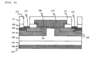
- an approximately 500 nm-thick Si oxide film 108 was formed on the front surface side of the SiC substrate using a CVD method, then, a region on which the gate insulating film 109 was to be formed was opened, and the front surface of the SiC substrate was locally exposed ( Fig. 4 ).
- the gate insulating film 109 formed in the example is formed of three film layers as illustrated in Fig. 6 .
- the SiC substrate was thermally treated at 1300°C in a NO gas atmosphere, and a 10 nm-thick Si oxynitride film 109a was formed.
- a 10 nm-thick alumina film 109b was formed using an atomic layer deposition (ALD method) in which trimethylaluminum (TMA) and ozone (O 3 ) were used as raw material gas.
- ALD method atomic layer deposition
- Si oxide film 109c was formed using a CVD method in which dichlorosilane (SiH 2 Cl 2 ) and nitrous oxide (N 2 O) were used as raw material gas, and then wet-oxidization was carried out at 850°C for 10 minutes, thereby reforming the Si oxide film 109c.
- the Si oxynitride film 109a on the bottom layer is the bottom barrier film 109a
- the Si oxide film 109c on the top layer is the top barrier film 109c
- the aluminum film 109b in the middle layer is the charge retention film 109b ( Figs. 5 and 6 ).
- specimens in which the film thickness of the bottom barrier film was 5 nm and the film thickness of the top barrier film was 40 nm were also produced.
- the electrical film thickness of the above-described three-layer laminated film in terms of the Si oxide film was approximately 50 nm.
- the concentration of nitrogen in the bulk region is extremely small, and most of nitrogen is present at the SiC interface. Nitrogen present at the SiC interface decreases the interface state density at the interface in the 4H-SiC substrate. In the studies, in a case in which a thermal treatment was carried out at 1300°C in a high-concentration NO atmosphere (approximately 90%), the concentration of nitrogen at the interface in the SiC substrate was approximately 1%.
- a phosphorous (P)-doped polycrystalline Si film was produced using a high-temperature thermal treatment.
- the phosphorous-doped polycrystalline Si film was processed using lithography and a dry etching technique so as to produce the gate electrode 110.
- some of the gate insulating film 109 below the gate electrode 110 was removed using dry etching. Consideration is given so that edges of the gate electrode 110 in the DiMOSFET formed in the example are processed on the thick Si oxide film 108 as illustrated in Fig. 7 so as to prevent the reliability of the gate insulating film 109 from deteriorating.
- an opening portion 112 through which the SiC-based high-concentration p-type diffusion layer 104 and the high-concentration n-type diffusion layer 105 are exposed at the same time was formed.
- nickel silicide 113 and 114 were formed on the front surface of the diffusion layer on the bottom of the opening portion 112 and the rear surface of the SiC substrate ( Fig. 8 ).
- an opening portion through which the front surface of the gate electrode 110 was exposed was formed afterwards.
- a current is made to flow from the gate electrode side or the SiC substrate side toward the gate insulating film, and some electrons are trapped.
- the degree of the threshold voltage shifted by electrons trapped in the gate insulating film is set using a voltage applied from outside and the time.
- Fig. 9 is a view illustrating the comparison of the Vg-Id characteristics between specimens in which the implanted channel was formed (counter N injection) and specimens in which the implanted channel was not formed.
- Solid lines A and A' in the drawing represent the initial characteristics of the specimens before injecting electrons into the gate insulating film.
- Broken lines B and B' represent the characteristics of the specimens after injecting electrons into the gate insulating film.
- Electrons were injected into the laminated gate insulating films by fixing the source electrode 115 and the drain electrode 114 to 0 V, and applying 38 V of a direct voltage (DC) of a pulse to the gate electrode 110.
- the pulse width was set to 100 nanoseconds, and the threshold voltage was adjusted so as to become almost identical.
- the example applies a combination of the implanted channel and a technique to inject carriers (electrons) into the gate insulating film having an electron-trapping property to the SiC nMOSFET.
- the gate insulating film preferably includes a laminated film in which Si oxide films or Si oxynitride films are made to sandwich a charge retention film in the middle portion from top and bottom, and serve as barrier (potential barrier) films.
- barrier potential barrier
- the film thickness of the barrier films is an extremely important parameter since the film thickness determines the charge-trapping characteristics (retention characteristics).
- SiC has lower dielectric breakdown strength than Si oxide films, and therefore SiC serves as a principal factor that determines the dielectric breakdown strength of the entire MOSFET (limits the dielectric breakdown conditions). Therefore, in the case of the SiC-MOSFET, unlike a Si-MOSFET, it is necessary to seek means for decreasing the dielectric breakdown strength applied to the barrier films.
- the top barrier film was made to be thicker than the bottom barrier film, thereby improving the reliability of the insulating film and the retention characteristics.
- the threshold voltage Vth shift becomes larger as the film thickness of the top barrier film increases.
- the film thickness of the top barrier film increases, it is possible to decrease the number of trapped electrons.
- a CVD film having lower insulation breakdown field strength than a thermally-oxidized film obtained by directly thermally oxidizing SiC the degree of freedom in design and process also improves.
- the top barrier film is made to be thick, relatively, a large electric field is applied to the bottom barrier film. Therefore, the use of a Si oxide film obtained by directly thermally oxidizing SiC having high insulation breakdown field strength or a Si oxide film obtained by thermally treating a CVD film for the bottom barrier film becomes preferable in terms of reliability.
- the film thickness of each barrier film is also extremely important since the film thickness determines the charge-trapping characteristics (retention characteristics).
- the important factors are a high temperature and the prevention of a change in the threshold voltage in a bias application state.
- Fig. 12 illustrates two retention characteristics in a case in which the bottom barrier film thicknesses of the n-DiMOSFET are set to 5 nm and 10 nm.
- the characteristics are the results obtained when an ONO film is used as the structure of the gate insulating film, in a case in which the film thickness of the bottom barrier film is 5 nm, the thickness of the top barrier film is set to 40 nm and the thickness of the charge-trapping film is set to 5 nm, in a case in which the film thickness of the bottom barrier film is 10 nm, the thickness of the top barrier film is set to 35 nm and the thickness of the charge-trapping film is set to 5 nm, and a stress electric field (an electric field applied to the gate insulating film during the operation of the SiC DiMOSFET) of 3 MV/cm is applied to the gate insulating film in an operation environment of 175°C.
- a stress electric field an electric field applied to the gate insulating film during the operation of the SiC DiMOSFET
- the thickness of the bottom barrier film is preferably 10 nm or more.
- the thickness of the charge-trapping film is set to 5 nm or more, it is possible to improve the retention characteristics.
- the thickness of the gate insulating film is 25 nm or more
- the thickness of the barrier films that sandwich the charge-trapping film is 10 nm or more
- the top barrier film is made to be thicker than the bottom barrier film, it is possible to obtain favorable retention characteristics.
- the material of the laminated film is also extremely important since the material determines the charge-trapping characteristics (retention characteristics).
- the barrier films are preferably Si oxide films or Si oxynitride films, and the charge-trapping film is preferably a Si nitride film or an alumina film (High-k film) since the electron trapping level is present at 1 eV or more deeper than the conduction band, and extremely stable trapping characteristics are exhibited.
- an alumina film serving as the charge-trapping film is preferable since the alumina film has more favorable retention characteristics than Si nitride film.
- the Si nitride film includes positive fixed charges, and the alumina film includes negative fixed charges.
- the alumina film having negative fixed charges exhibits a large value. Therefore, the use of the alumina film can decrease the number of electrons being trapped.
- the barrier film particularly, as the bottom barrier film, it is preferable to use a Si oxide film in which the composition ratio of Si:O can be approximated to 1:2, a Si oxynitride film formed through a oxynitriding treatment in a high-temperature NO atmosphere, a Si oxynitride film formed by oxynitriding a Si oxide film formed using a chemical vapor deposition method (CVD method) in a high-temperature NO atmosphere, or a Si oxynitride film formed by directly oxynitriding a SiC substrate in a high-temperature NO atmosphere, such as a Si oxide film formed by thermally oxidizing a SiC substrate and a thermally-oxidized CVD-Si oxide film (P-CVD film, thermal CVD film or photo CVD film).
- CVD method chemical vapor deposition method
- the interface state at the interface in the SiC substrate is decreased due to a NO oxynitriding treatment so that the mobility improves, and it is possible to obtain favorable reliability of the insulating film or favorable retention characteristics as described above.
- a Si oxide film that is significantly decomposed into a composition ratio of Si:O of 1:2 such as a Si oxide film produced using P-CVD that does not undergo a high-temperature step (that is not thermally oxidized) is used
- the mobility is extremely low, the retention characteristics cannot be held at a high gate voltage Vg, which is for high-voltage use (600 [V] or more), and there is a possibility of some of the trapped electrons being discharged.
- the impurity concentration or depth (thickness) of nitrogen is preferably a concentration that is slightly larger than or almost the same as the concentration of aluminum in the vicinity of the front surface of the p-type body region, and the depth (thickness) is preferably in a range of approximately 30 nm to 150 nm.
- the depth (thickness from the interface) of the implanted n-type layer is set to approximately 30 nm or more, it becomes possible to significantly suppress the influence of the interface state at the interface in the SiC substrate.
- the threshold voltage Vth and the gate voltage Vg also need to be increased by that amount; however, when the depth is approximately 150 nm or less, the channel control using the gate electric field is possible.
- the injection of nitrogen ions was used to form the implanted channel layer, but the same effects could be obtained as well when a low-concentration n-type SiC layer was formed using a SiC homoepitaxial method.
- a step of carrying out electron injection on the gate insulating film was carried out at a wafer level after the completion of the device, but it is needless to say that the step can be carried out after chip dicing or after package assembly.
- electrons were injected from the SiC substrate side, but it is also possible to inject electrons from the gate electrode side by applying the gate electrode to a negative bias.
- the present example describes an example of the SiC DiMOSFET, but the invention can also be applied to trench MOSFETs as long as the trench MOSFETs are SiC MOSFETs having an implanted channel.
Landscapes
- Insulated Gate Type Field-Effect Transistor (AREA)
- Formation Of Insulating Films (AREA)
- Electrodes Of Semiconductors (AREA)
Applications Claiming Priority (1)
| Application Number | Priority Date | Filing Date | Title |
|---|---|---|---|
| PCT/JP2012/002224 WO2013145023A1 (fr) | 2012-03-30 | 2012-03-30 | Transistor à effet de champ en carbure de silicium |
Publications (2)
| Publication Number | Publication Date |
|---|---|
| EP2833409A1 true EP2833409A1 (fr) | 2015-02-04 |
| EP2833409A4 EP2833409A4 (fr) | 2015-11-11 |
Family
ID=49258396
Family Applications (1)
| Application Number | Title | Priority Date | Filing Date |
|---|---|---|---|
| EP12873344.1A Withdrawn EP2833409A4 (fr) | 2012-03-30 | 2012-03-30 | Transistor à effet de champ en carbure de silicium |
Country Status (4)
| Country | Link |
|---|---|
| US (1) | US9214516B2 (fr) |
| EP (1) | EP2833409A4 (fr) |
| JP (1) | JP5982471B2 (fr) |
| WO (1) | WO2013145023A1 (fr) |
Cited By (1)
| Publication number | Priority date | Publication date | Assignee | Title |
|---|---|---|---|---|
| WO2019159680A1 (fr) * | 2018-02-16 | 2019-08-22 | Toyota Jidosha Kabushiki Kaisha | Procédé de fabrication de dispositif à semi-conducteurs au carbure de silicium et dispositif à semi-conducteurs au carbure de silicium |
Families Citing this family (11)
| Publication number | Priority date | Publication date | Assignee | Title |
|---|---|---|---|---|
| US11721547B2 (en) * | 2013-03-14 | 2023-08-08 | Infineon Technologies Ag | Method for manufacturing a silicon carbide substrate for an electrical silicon carbide device, a silicon carbide substrate and an electrical silicon carbide device |
| JP2016066641A (ja) * | 2014-09-22 | 2016-04-28 | 株式会社東芝 | 半導体装置及び半導体装置の製造方法 |
| US9553155B2 (en) * | 2015-02-04 | 2017-01-24 | Infineon Technologies Austria Ag | Semiconductor device and method |
| JP6711102B2 (ja) * | 2016-04-19 | 2020-06-17 | 富士電機株式会社 | 絶縁ゲート型半導体装置及び絶縁ゲート型半導体装置の製造方法 |
| JP6884532B2 (ja) | 2016-09-02 | 2021-06-09 | 住友電気工業株式会社 | SiC構造体の製造方法 |
| KR102783331B1 (ko) * | 2017-02-02 | 2025-03-20 | 삼성디스플레이 주식회사 | 유기 발광 표시 장치 |
| US20220028984A1 (en) * | 2020-11-12 | 2022-01-27 | Hua Hong Semiconductor (Wuxi) Limited | Interlayer dielectric layer structure for power mos device and method for making the same |
| JP7704661B2 (ja) * | 2021-12-02 | 2025-07-08 | 株式会社デンソー | スイッチング素子とその製造方法 |
| CN116705605B (zh) * | 2023-06-20 | 2024-06-18 | 中国科学院上海微系统与信息技术研究所 | 一种硅基氮化镓hemt器件及其制备方法 |
| CN116936620A (zh) * | 2023-09-14 | 2023-10-24 | 凌锐半导体(上海)有限公司 | 一种碳化硅沟槽栅mosfet的制备方法 |
| WO2025196983A1 (fr) * | 2024-03-19 | 2025-09-25 | サンケン電気株式会社 | Dispositif à semi-conducteurs au carbure de silicium et procédé de fabrication de dispositif à semi-conducteurs au carbure de silicium |
Family Cites Families (19)
| Publication number | Priority date | Publication date | Assignee | Title |
|---|---|---|---|---|
| KR940004847A (ko) * | 1992-08-04 | 1994-03-16 | 리차드 제이. 컬 | 낮은 드레쉬 홀드 전압을 갖는 에피택셜 이중 확산형 금속 산화 실리콘(dmos) 트랜지스터 구조체 형성방법 |
| US6956238B2 (en) | 2000-10-03 | 2005-10-18 | Cree, Inc. | Silicon carbide power metal-oxide semiconductor field effect transistors having a shorting channel and methods of fabricating silicon carbide metal-oxide semiconductor field effect transistors having a shorting channel |
| JP2002222950A (ja) * | 2001-01-25 | 2002-08-09 | Denso Corp | 炭化珪素半導体装置の製造方法 |
| WO2003047000A1 (fr) * | 2001-11-30 | 2003-06-05 | Matsushita Electric Industrial Co., Ltd. | Dispositif à semi-conducteur et procédé de fabrication |
| JP2005183943A (ja) * | 2003-11-25 | 2005-07-07 | Matsushita Electric Ind Co Ltd | 半導体素子 |
| CN1802752A (zh) | 2003-11-25 | 2006-07-12 | 松下电器产业株式会社 | 半导体元件 |
| JP2007066944A (ja) * | 2005-08-29 | 2007-03-15 | Nissan Motor Co Ltd | 炭化珪素半導体装置及びその製造方法 |
| JP2008244455A (ja) * | 2007-02-28 | 2008-10-09 | Denso Corp | 炭化珪素半導体装置およびその製造方法 |
| JP2008270258A (ja) | 2007-04-16 | 2008-11-06 | Denso Corp | 半導体装置の製造方法 |
| CN100590804C (zh) * | 2007-06-22 | 2010-02-17 | 中芯国际集成电路制造(上海)有限公司 | 原子层沉积方法以及形成的半导体器件 |
| WO2009013886A1 (fr) * | 2007-07-20 | 2009-01-29 | Panasonic Corporation | Dispositif semi-conducteur au carbure de silicium et son procédé de fabrication |
| CN101569015B (zh) * | 2007-10-15 | 2011-01-05 | 松下电器产业株式会社 | 半导体装置及其制造方法 |
| JP2009141144A (ja) | 2007-12-06 | 2009-06-25 | Sharp Corp | 半導体記憶装置及びその製造方法と駆動方法 |
| CN102414818B (zh) * | 2009-04-30 | 2013-03-20 | 松下电器产业株式会社 | 半导体元件、半导体装置及电力变换器 |
| JP2011091186A (ja) | 2009-10-22 | 2011-05-06 | Mitsubishi Electric Corp | 炭化珪素半導体装置の製造方法 |
| JP2012004269A (ja) | 2010-06-16 | 2012-01-05 | Sumitomo Electric Ind Ltd | 炭化珪素半導体装置の製造方法および炭化珪素半導体装置の製造装置 |
| US20120019284A1 (en) * | 2010-07-26 | 2012-01-26 | Infineon Technologies Austria Ag | Normally-Off Field Effect Transistor, a Manufacturing Method Therefor and a Method for Programming a Power Field Effect Transistor |
| JP5961865B2 (ja) | 2010-09-15 | 2016-08-02 | ローム株式会社 | 半導体素子 |
| WO2014010006A1 (fr) * | 2012-07-09 | 2014-01-16 | 株式会社日立製作所 | Transistor à effet de champ mos |
-
2012
- 2012-03-30 WO PCT/JP2012/002224 patent/WO2013145023A1/fr not_active Ceased
- 2012-03-30 JP JP2014507015A patent/JP5982471B2/ja not_active Expired - Fee Related
- 2012-03-30 EP EP12873344.1A patent/EP2833409A4/fr not_active Withdrawn
- 2012-03-30 US US14/240,376 patent/US9214516B2/en not_active Expired - Fee Related
Cited By (4)
| Publication number | Priority date | Publication date | Assignee | Title |
|---|---|---|---|---|
| WO2019159680A1 (fr) * | 2018-02-16 | 2019-08-22 | Toyota Jidosha Kabushiki Kaisha | Procédé de fabrication de dispositif à semi-conducteurs au carbure de silicium et dispositif à semi-conducteurs au carbure de silicium |
| CN111788661A (zh) * | 2018-02-16 | 2020-10-16 | 株式会社电装 | 碳化硅半导体器件的制造方法和碳化硅半导体器件 |
| US11501971B2 (en) | 2018-02-16 | 2022-11-15 | Denso Corporation | Manufacturing method of silicon carbide semiconductor device and silicon carbide semiconductor device |
| CN111788661B (zh) * | 2018-02-16 | 2024-03-22 | 株式会社电装 | 碳化硅半导体器件的制造方法和碳化硅半导体器件 |
Also Published As
| Publication number | Publication date |
|---|---|
| EP2833409A4 (fr) | 2015-11-11 |
| WO2013145023A1 (fr) | 2013-10-03 |
| JPWO2013145023A1 (ja) | 2015-08-03 |
| US20140217422A1 (en) | 2014-08-07 |
| US9214516B2 (en) | 2015-12-15 |
| JP5982471B2 (ja) | 2016-08-31 |
Similar Documents
| Publication | Publication Date | Title |
|---|---|---|
| US9214516B2 (en) | Field effect silicon carbide transistor | |
| US9812529B2 (en) | Semiconductor device and method for manufacturing the same | |
| JP5875684B2 (ja) | Mos型電界効果トランジスタ | |
| US7221010B2 (en) | Vertical JFET limited silicon carbide power metal-oxide semiconductor field effect transistors | |
| US9478655B2 (en) | Semiconductor device having a lower diode region arranged below a trench | |
| US9837527B2 (en) | Semiconductor device with a trench electrode | |
| EP2740148B1 (fr) | Formation de transistors mosfet à base de sic à canaux haute à haute mobilité par traitement de l'interface d'oxyde avec des ions césium | |
| US9000448B2 (en) | Silicon carbide semiconductor device | |
| US9755064B2 (en) | Semiconductor device and method for manufacturing the same | |
| TW201241993A (en) | Silicon carbide semiconductor device | |
| US9978842B2 (en) | Semiconductor device and method for manufacturing the same | |
| JP7150609B2 (ja) | 短チャネルのトレンチパワーmosfet | |
| US20130248880A1 (en) | Semiconductor device and method for manufacturing the same | |
| WO2015015672A1 (fr) | Dispositif à semi-conducteur au carbure de silicium et son procédé de fabrication | |
| JP6500912B2 (ja) | 炭化珪素半導体装置および炭化珪素半導体装置の製造方法 | |
| JP2010027833A (ja) | 炭化珪素半導体装置およびその製造方法 | |
| JP7697210B2 (ja) | 炭化珪素半導体装置および炭化珪素半導体装置の製造方法 | |
| JP6270667B2 (ja) | 半導体装置及びその製造方法 | |
| JP2017168680A (ja) | 炭化珪素半導体装置および炭化珪素半導体装置の製造方法 | |
| WO2023112312A1 (fr) | Dispositif à semi-conducteur et son procédé de fabrication | |
| Chowdhury et al. | Effect of Activation Annealing and Reactive Ion Etching on MOS Channel Properties of (11-20) Oriented 4H-SiC |
Legal Events
| Date | Code | Title | Description |
|---|---|---|---|
| PUAI | Public reference made under article 153(3) epc to a published international application that has entered the european phase |
Free format text: ORIGINAL CODE: 0009012 |
|
| 17P | Request for examination filed |
Effective date: 20140314 |
|
| AK | Designated contracting states |
Kind code of ref document: A1 Designated state(s): AL AT BE BG CH CY CZ DE DK EE ES FI FR GB GR HR HU IE IS IT LI LT LU LV MC MK MT NL NO PL PT RO RS SE SI SK SM TR |
|
| AX | Request for extension of the european patent |
Extension state: BA ME |
|
| DAX | Request for extension of the european patent (deleted) | ||
| RA4 | Supplementary search report drawn up and despatched (corrected) |
Effective date: 20151008 |
|
| RIC1 | Information provided on ipc code assigned before grant |
Ipc: H01L 29/792 20060101ALI20151002BHEP Ipc: H01L 29/51 20060101ALI20151002BHEP Ipc: H01L 29/78 20060101AFI20151002BHEP Ipc: H01L 29/16 20060101ALI20151002BHEP |
|
| STAA | Information on the status of an ep patent application or granted ep patent |
Free format text: STATUS: EXAMINATION IS IN PROGRESS |
|
| 17Q | First examination report despatched |
Effective date: 20190410 |
|
| STAA | Information on the status of an ep patent application or granted ep patent |
Free format text: STATUS: THE APPLICATION IS DEEMED TO BE WITHDRAWN |
|
| 18D | Application deemed to be withdrawn |
Effective date: 20190821 |