EP2833461A1 - Herstellungsverfahren einer Lithium-Mikrobatterie - Google Patents
Herstellungsverfahren einer Lithium-Mikrobatterie Download PDFInfo
- Publication number
- EP2833461A1 EP2833461A1 EP14178955.2A EP14178955A EP2833461A1 EP 2833461 A1 EP2833461 A1 EP 2833461A1 EP 14178955 A EP14178955 A EP 14178955A EP 2833461 A1 EP2833461 A1 EP 2833461A1
- Authority
- EP
- European Patent Office
- Prior art keywords
- layer
- pattern
- lithium
- etching
- microbattery
- Prior art date
- Legal status (The legal status is an assumption and is not a legal conclusion. Google has not performed a legal analysis and makes no representation as to the accuracy of the status listed.)
- Granted
Links
Images


Classifications
-
- H—ELECTRICITY
- H01—ELECTRIC ELEMENTS
- H01M—PROCESSES OR MEANS, e.g. BATTERIES, FOR THE DIRECT CONVERSION OF CHEMICAL ENERGY INTO ELECTRICAL ENERGY
- H01M4/00—Electrodes
- H01M4/02—Electrodes composed of, or comprising, active material
- H01M4/13—Electrodes for accumulators with non-aqueous electrolyte, e.g. for lithium-accumulators; Processes of manufacture thereof
- H01M4/139—Processes of manufacture
- H01M4/1395—Processes of manufacture of electrodes based on metals, Si or alloys
-
- H—ELECTRICITY
- H01—ELECTRIC ELEMENTS
- H01M—PROCESSES OR MEANS, e.g. BATTERIES, FOR THE DIRECT CONVERSION OF CHEMICAL ENERGY INTO ELECTRICAL ENERGY
- H01M10/00—Secondary cells; Manufacture thereof
- H01M10/05—Accumulators with non-aqueous electrolyte
- H01M10/052—Li-accumulators
-
- H—ELECTRICITY
- H01—ELECTRIC ELEMENTS
- H01M—PROCESSES OR MEANS, e.g. BATTERIES, FOR THE DIRECT CONVERSION OF CHEMICAL ENERGY INTO ELECTRICAL ENERGY
- H01M10/00—Secondary cells; Manufacture thereof
- H01M10/05—Accumulators with non-aqueous electrolyte
- H01M10/056—Accumulators with non-aqueous electrolyte characterised by the materials used as electrolytes, e.g. mixed inorganic/organic electrolytes
- H01M10/0561—Accumulators with non-aqueous electrolyte characterised by the materials used as electrolytes, e.g. mixed inorganic/organic electrolytes the electrolyte being constituted of inorganic materials only
- H01M10/0562—Solid materials
-
- H—ELECTRICITY
- H01—ELECTRIC ELEMENTS
- H01M—PROCESSES OR MEANS, e.g. BATTERIES, FOR THE DIRECT CONVERSION OF CHEMICAL ENERGY INTO ELECTRICAL ENERGY
- H01M10/00—Secondary cells; Manufacture thereof
- H01M10/05—Accumulators with non-aqueous electrolyte
- H01M10/058—Construction or manufacture
- H01M10/0585—Construction or manufacture of accumulators having only flat construction elements, i.e. flat positive electrodes, flat negative electrodes and flat separators
-
- H—ELECTRICITY
- H01—ELECTRIC ELEMENTS
- H01M—PROCESSES OR MEANS, e.g. BATTERIES, FOR THE DIRECT CONVERSION OF CHEMICAL ENERGY INTO ELECTRICAL ENERGY
- H01M10/00—Secondary cells; Manufacture thereof
- H01M10/36—Accumulators not provided for in groups H01M10/05-H01M10/34
- H01M10/38—Construction or manufacture
-
- H—ELECTRICITY
- H01—ELECTRIC ELEMENTS
- H01M—PROCESSES OR MEANS, e.g. BATTERIES, FOR THE DIRECT CONVERSION OF CHEMICAL ENERGY INTO ELECTRICAL ENERGY
- H01M4/00—Electrodes
- H01M4/02—Electrodes composed of, or comprising, active material
- H01M4/04—Processes of manufacture in general
- H01M4/0402—Methods of deposition of the material
- H01M4/0407—Methods of deposition of the material by coating on an electrolyte layer
-
- H—ELECTRICITY
- H01—ELECTRIC ELEMENTS
- H01M—PROCESSES OR MEANS, e.g. BATTERIES, FOR THE DIRECT CONVERSION OF CHEMICAL ENERGY INTO ELECTRICAL ENERGY
- H01M4/00—Electrodes
- H01M4/02—Electrodes composed of, or comprising, active material
- H01M4/04—Processes of manufacture in general
- H01M4/049—Manufacturing of an active layer by chemical means
- H01M4/0492—Chemical attack of the support material
-
- H—ELECTRICITY
- H01—ELECTRIC ELEMENTS
- H01M—PROCESSES OR MEANS, e.g. BATTERIES, FOR THE DIRECT CONVERSION OF CHEMICAL ENERGY INTO ELECTRICAL ENERGY
- H01M4/00—Electrodes
- H01M4/02—Electrodes composed of, or comprising, active material
- H01M4/36—Selection of substances as active materials, active masses, active liquids
- H01M4/38—Selection of substances as active materials, active masses, active liquids of elements or alloys
- H01M4/381—Alkaline or alkaline earth metals elements
- H01M4/382—Lithium
-
- H—ELECTRICITY
- H01—ELECTRIC ELEMENTS
- H01M—PROCESSES OR MEANS, e.g. BATTERIES, FOR THE DIRECT CONVERSION OF CHEMICAL ENERGY INTO ELECTRICAL ENERGY
- H01M6/00—Primary cells; Manufacture thereof
- H01M6/04—Cells with aqueous electrolyte
- H01M6/045—Cells with aqueous electrolyte characterised by aqueous electrolyte
-
- H—ELECTRICITY
- H01—ELECTRIC ELEMENTS
- H01M—PROCESSES OR MEANS, e.g. BATTERIES, FOR THE DIRECT CONVERSION OF CHEMICAL ENERGY INTO ELECTRICAL ENERGY
- H01M6/00—Primary cells; Manufacture thereof
- H01M6/14—Cells with non-aqueous electrolyte
- H01M6/18—Cells with non-aqueous electrolyte with solid electrolyte
- H01M6/185—Cells with non-aqueous electrolyte with solid electrolyte with oxides, hydroxides or oxysalts as solid electrolytes
- H01M6/186—Only oxysalts-containing solid electrolytes
-
- H—ELECTRICITY
- H01—ELECTRIC ELEMENTS
- H01M—PROCESSES OR MEANS, e.g. BATTERIES, FOR THE DIRECT CONVERSION OF CHEMICAL ENERGY INTO ELECTRICAL ENERGY
- H01M6/00—Primary cells; Manufacture thereof
- H01M6/14—Cells with non-aqueous electrolyte
- H01M6/18—Cells with non-aqueous electrolyte with solid electrolyte
- H01M6/187—Solid electrolyte characterised by the form
-
- H—ELECTRICITY
- H01—ELECTRIC ELEMENTS
- H01M—PROCESSES OR MEANS, e.g. BATTERIES, FOR THE DIRECT CONVERSION OF CHEMICAL ENERGY INTO ELECTRICAL ENERGY
- H01M6/00—Primary cells; Manufacture thereof
- H01M6/40—Printed batteries, e.g. thin film batteries
-
- B—PERFORMING OPERATIONS; TRANSPORTING
- B81—MICROSTRUCTURAL TECHNOLOGY
- B81C—PROCESSES OR APPARATUS SPECIALLY ADAPTED FOR THE MANUFACTURE OR TREATMENT OF MICROSTRUCTURAL DEVICES OR SYSTEMS
- B81C1/00—Manufacture or treatment of devices or systems in or on a substrate
- B81C1/00388—Etch mask forming
- B81C1/00396—Mask characterised by its composition, e.g. multilayer masks
-
- B—PERFORMING OPERATIONS; TRANSPORTING
- B81—MICROSTRUCTURAL TECHNOLOGY
- B81C—PROCESSES OR APPARATUS SPECIALLY ADAPTED FOR THE MANUFACTURE OR TREATMENT OF MICROSTRUCTURAL DEVICES OR SYSTEMS
- B81C1/00—Manufacture or treatment of devices or systems in or on a substrate
- B81C1/00388—Etch mask forming
- B81C1/00412—Mask characterised by its behaviour during the etching process, e.g. soluble masks
-
- C—CHEMISTRY; METALLURGY
- C09—DYES; PAINTS; POLISHES; NATURAL RESINS; ADHESIVES; COMPOSITIONS NOT OTHERWISE PROVIDED FOR; APPLICATIONS OF MATERIALS NOT OTHERWISE PROVIDED FOR
- C09K—MATERIALS FOR MISCELLANEOUS APPLICATIONS, NOT PROVIDED FOR ELSEWHERE
- C09K13/00—Etching, surface-brightening or pickling compositions
- C09K13/04—Etching, surface-brightening or pickling compositions containing an inorganic acid
-
- C—CHEMISTRY; METALLURGY
- C23—COATING METALLIC MATERIAL; COATING MATERIAL WITH METALLIC MATERIAL; CHEMICAL SURFACE TREATMENT; DIFFUSION TREATMENT OF METALLIC MATERIAL; COATING BY VACUUM EVAPORATION, BY SPUTTERING, BY ION IMPLANTATION OR BY CHEMICAL VAPOUR DEPOSITION, IN GENERAL; INHIBITING CORROSION OF METALLIC MATERIAL OR INCRUSTATION IN GENERAL
- C23F—NON-MECHANICAL REMOVAL OF METALLIC MATERIAL FROM SURFACE; INHIBITING CORROSION OF METALLIC MATERIAL OR INCRUSTATION IN GENERAL; MULTI-STEP PROCESSES FOR SURFACE TREATMENT OF METALLIC MATERIAL INVOLVING AT LEAST ONE PROCESS PROVIDED FOR IN CLASS C23 AND AT LEAST ONE PROCESS COVERED BY SUBCLASS C21D OR C22F OR CLASS C25
- C23F1/00—Etching metallic material by chemical means
- C23F1/02—Local etching
-
- C—CHEMISTRY; METALLURGY
- C23—COATING METALLIC MATERIAL; COATING MATERIAL WITH METALLIC MATERIAL; CHEMICAL SURFACE TREATMENT; DIFFUSION TREATMENT OF METALLIC MATERIAL; COATING BY VACUUM EVAPORATION, BY SPUTTERING, BY ION IMPLANTATION OR BY CHEMICAL VAPOUR DEPOSITION, IN GENERAL; INHIBITING CORROSION OF METALLIC MATERIAL OR INCRUSTATION IN GENERAL
- C23F—NON-MECHANICAL REMOVAL OF METALLIC MATERIAL FROM SURFACE; INHIBITING CORROSION OF METALLIC MATERIAL OR INCRUSTATION IN GENERAL; MULTI-STEP PROCESSES FOR SURFACE TREATMENT OF METALLIC MATERIAL INVOLVING AT LEAST ONE PROCESS PROVIDED FOR IN CLASS C23 AND AT LEAST ONE PROCESS COVERED BY SUBCLASS C21D OR C22F OR CLASS C25
- C23F4/00—Processes for removing metallic material from surfaces, not provided for in group C23F1/00 or C23F3/00
-
- G—PHYSICS
- G03—PHOTOGRAPHY; CINEMATOGRAPHY; ANALOGOUS TECHNIQUES USING WAVES OTHER THAN OPTICAL WAVES; ELECTROGRAPHY; HOLOGRAPHY
- G03F—PHOTOMECHANICAL PRODUCTION OF TEXTURED OR PATTERNED SURFACES, e.g. FOR PRINTING, FOR PROCESSING OF SEMICONDUCTOR DEVICES; MATERIALS THEREFOR; ORIGINALS THEREFOR; APPARATUS SPECIALLY ADAPTED THEREFOR
- G03F7/00—Photomechanical, e.g. photolithographic, production of textured or patterned surfaces, e.g. printing surfaces; Materials therefor, e.g. comprising photoresists; Apparatus specially adapted therefor
- G03F7/004—Photosensitive materials
- G03F7/09—Photosensitive materials characterised by structural details, e.g. supports, auxiliary layers
- G03F7/094—Multilayer resist systems, e.g. planarising layers
-
- H—ELECTRICITY
- H01—ELECTRIC ELEMENTS
- H01M—PROCESSES OR MEANS, e.g. BATTERIES, FOR THE DIRECT CONVERSION OF CHEMICAL ENERGY INTO ELECTRICAL ENERGY
- H01M2300/00—Electrolytes
- H01M2300/0002—Aqueous electrolytes
-
- H—ELECTRICITY
- H01—ELECTRIC ELEMENTS
- H01M—PROCESSES OR MEANS, e.g. BATTERIES, FOR THE DIRECT CONVERSION OF CHEMICAL ENERGY INTO ELECTRICAL ENERGY
- H01M4/00—Electrodes
- H01M4/02—Electrodes composed of, or comprising, active material
- H01M4/04—Processes of manufacture in general
- H01M4/0402—Methods of deposition of the material
- H01M4/0421—Methods of deposition of the material involving vapour deposition
-
- H—ELECTRICITY
- H01—ELECTRIC ELEMENTS
- H01M—PROCESSES OR MEANS, e.g. BATTERIES, FOR THE DIRECT CONVERSION OF CHEMICAL ENERGY INTO ELECTRICAL ENERGY
- H01M4/00—Electrodes
- H01M4/02—Electrodes composed of, or comprising, active material
- H01M4/04—Processes of manufacture in general
- H01M4/0402—Methods of deposition of the material
- H01M4/0421—Methods of deposition of the material involving vapour deposition
- H01M4/0423—Physical vapour deposition
- H01M4/0426—Sputtering
-
- H—ELECTRICITY
- H01—ELECTRIC ELEMENTS
- H01M—PROCESSES OR MEANS, e.g. BATTERIES, FOR THE DIRECT CONVERSION OF CHEMICAL ENERGY INTO ELECTRICAL ENERGY
- H01M4/00—Electrodes
- H01M4/02—Electrodes composed of, or comprising, active material
- H01M4/04—Processes of manufacture in general
- H01M4/0438—Processes of manufacture in general by electrochemical processing
- H01M4/045—Electrochemical coating; Electrochemical impregnation
-
- Y—GENERAL TAGGING OF NEW TECHNOLOGICAL DEVELOPMENTS; GENERAL TAGGING OF CROSS-SECTIONAL TECHNOLOGIES SPANNING OVER SEVERAL SECTIONS OF THE IPC; TECHNICAL SUBJECTS COVERED BY FORMER USPC CROSS-REFERENCE ART COLLECTIONS [XRACs] AND DIGESTS
- Y02—TECHNOLOGIES OR APPLICATIONS FOR MITIGATION OR ADAPTATION AGAINST CLIMATE CHANGE
- Y02E—REDUCTION OF GREENHOUSE GAS [GHG] EMISSIONS, RELATED TO ENERGY GENERATION, TRANSMISSION OR DISTRIBUTION
- Y02E60/00—Enabling technologies; Technologies with a potential or indirect contribution to GHG emissions mitigation
- Y02E60/10—Energy storage using batteries
-
- Y—GENERAL TAGGING OF NEW TECHNOLOGICAL DEVELOPMENTS; GENERAL TAGGING OF CROSS-SECTIONAL TECHNOLOGIES SPANNING OVER SEVERAL SECTIONS OF THE IPC; TECHNICAL SUBJECTS COVERED BY FORMER USPC CROSS-REFERENCE ART COLLECTIONS [XRACs] AND DIGESTS
- Y02—TECHNOLOGIES OR APPLICATIONS FOR MITIGATION OR ADAPTATION AGAINST CLIMATE CHANGE
- Y02P—CLIMATE CHANGE MITIGATION TECHNOLOGIES IN THE PRODUCTION OR PROCESSING OF GOODS
- Y02P70/00—Climate change mitigation technologies in the production process for final industrial or consumer products
- Y02P70/50—Manufacturing or production processes characterised by the final manufactured product
Definitions
- the invention relates to the structuring of a solid electrolyte layer for, in particular, making a lithium microbattery.
- a lithium microbattery is an electrochemical accumulator involving Li + ions and comprising an active stack of thin layers.
- the active stack is formed by two electrodes, one positive and one negative, separated by a solid electrolyte.
- the solid electrolyte is an electrical insulator with a high ionic conductivity.
- the solid electrolyte is generally based on a lithiated compound.
- the positive electrode is a lithium insertion material, for example lithium metal oxides.
- the so-called lithium-metal lithium microbatteries comprise a negative lithium metal electrode.
- the so-called “lithium-ion” lithium microbatteries comprise a negative electrode formed by a lithium intercalation or insertion material.
- Lithium microbatteries are particularly interesting because of their high mass density and their low toxicity. However, a lithium microbattery is very sensitive to air and moisture.
- the lithium-based layers are very reactive and very chemically unstable.
- the presence of lithium and, in some cases, sulfur in thin layers forming a microbattery gives these layers a strongly hygroscopic character and a chemical instability in the air.
- this type of thin layers, in particular the solid electrolyte layers are difficult to structure.
- a conventional technique consists in successively depositing the thin layers of the micro-battery, in particular by vacuum deposition techniques.
- the structuring of a solid electrolyte layer is generally carried out using a mechanical masking ("shadow masking" according to English terminology).
- Deposition under vacuum PVD for example (“Physical Vapor Deposition”)
- PVD Physical Vapor Deposition
- the mask is placed on the substrate and held in position for the duration of the deposit. Then, the mechanical mask is removed and the substrate has the desired patterns.
- This masking technique generates particulate contamination, and the mechanical mask can also scratch the layer on which it is laid, thus potentially damaging the microbattery. Moreover, when the size of the microbattery is reduced, the mechanical mask can generate edge or shading effects that prove to be detrimental to the proper functioning of the microbattery.
- WO2012173874 discloses a method of making lithium microbatteries using a technique of structuring of lithium phosphorus oxynitride (LiPON) electrolyte layer by laser ablation.
- the thin layers forming the electrodes, and the current collectors are formed in a conventional manner using a deposition through a mechanical mask.
- the solid electrolyte is deposited without the use of a mechanical mask, and its structuring is carried out using a pulsed laser beam having a size of 1 mm 2 .
- the laser beam must scan all the useful surface of the substrate on which the microbatteries are made.
- this technique strongly depends on the substrate used as well as the nature of the layers deposited at lower levels.
- this method may require the use of different devices, which increases the risk of exposure of the solid electrolyte layer to air and moisture.
- the implementation of this production method is slow and complex.
- the subject of the invention is a method for producing a lithium microbattery which is easy to produce, inexpensive and compatible with the technologies used in the field of microelectronics.
- the etching of the uncovered zone of the electrolyte layer and the etching of the first pattern are advantageously carried out simultaneously.
- the etching of the second material is performed by plasma etching using the electrolyte layer as a stop layer of etching.
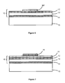
- the method comprises the provision of a stack 10 successively comprising a first layer 11 of the first material, a second layer 12 of the second material, a solid electrolyte layer 13 and a first electrode 14.
- the thin layers 12 to 14 are intended to form a lithium microbattery.
- the thin layers 11 to 14 may be successively deposited on a substrate 15 by conventional techniques of the microelectronic industry, for example by physical vapor deposition (PVD), deposition by evaporation under vacuum, chemical deposition. in the vapor phase (“Chemical Vapor Deposition", CVD).
- PVD physical vapor deposition
- CVD chemical Vapor Deposition
- the thickness of the thin layers 11 to 14 may vary between a few nanometers and a few tens of micrometers.
- the substrate 15 is generally a silicon wafer, which may comprise an integrated circuit.
- the substrate may also be glass or ceramic.
- the substrate 15 may be covered by a passivation layer, typically based on silicon oxide, or by a bilayer formed by an oxide layer and a silicon nitride layer.
- the substrate 15 can also form the first electrode 14.
- the first electrode 14 is generally a Li + ion generating electrode or comprising a lithium intercalation material.
- the material used as the active material of the first electrode 14 may be a non-lithiated material such as a vanadium oxide (V x O y ) or a titanium oxysulfide (TiO x S y ).
- the material of the electrode 14 may also be a lithiated material such as lithium cobalt oxide (LiCoO 2 ), lithium nickel oxide (LiNiO 2 ), etc.
- the substrate 15 may also comprise other thin layers, in particular layers forming current collectors of the microbattery.
- these current collectors are formed by metal layers, for example platinum, chromium, gold, titanium, etc.
- the step of producing these current collectors is independent of the step of forming the stack 10. In other words, the current collectors of the microbattery can be made before, during, or after the step of forming the collector. stacking 10.
- the solid electrolyte layer 13 is disposed on the first electrode 14.
- the solid electrolyte 13 is a layer permeable to lithium ions, and is preferably based on lithium. In other words, the electrolyte 13 is configured to allow the conduction of Li + lithium ions.
- the material of the solid electrolyte 13 is an electrically insulating material.
- the solid electrolyte 13 may be lithium boron oxynitride (LiBON), lithium silicophosphate oxynitride (LiSiPON), etc.
- the solid electrolyte 13 is phosphonium oxynitride and lithium (LiPON) called "lipon".
- the stack 10 also comprises a bilayer disposed on the solid electrolyte 13.
- the bilayer is formed by a first layer 11 of first material disposed on a second layer 12 of the second material.
- the bilayer is intended to form an etching mask for, in particular, structuring the solid electrolyte layer 13.
- the first layer 11 is a sacrificial layer, and it may be based on aluminum (Al), alumina (Al 2 O 3 ), titanium (Ti), nickel (Ni), chromium (Cr), etc.
- the second layer 12 is preferably based on a material configured to alloy with the lithium atoms, or at least to have a diffusion of the lithium atoms in the second layer 12.
- the second material may be based on silicon ( Si), germanium (Ge), tin (Sn), carbon (C), gold (Au), platinum (Pt), etc.
- the second layer 12 is configured to form a second electrode 16, of opposite polarity with respect to the first electrode 14.
- the thickness of the layers 11 and 12 is between a few nanometers and a few tens of nanometers, preferably between 5 and 100 nm.
- the method for producing a lithium microbattery also comprises a step of etching the first and second materials to form, as illustrated in FIG. figure 2 , first and second patterns M1 and M2.
- the first pattern M1 is in first material.
- the second pattern M2 is in second material, and it is configured to define a covered area 13 "and an open area 13 'of the solid electrolyte layer 13.
- the second layer 12, in particular the second pattern M2 advantageously provides to protect the electrolyte layer 13 and especially the interface between the solid electrolyte 13 and the second material during the various steps of producing the microbattery.
- the etching of the first and second materials is carried out by any known means, for example, by conventional techniques in the field of microelectronics and compatible with the first and second materials.
- the formation of the first and second patterns M1 and M2 is carried out by first etching the first material so as to define the first pattern M1 as the first material disposed on the second layer 13.
- the first M1 pattern is formed while the solid electrolyte 13 is protected by the second layer 12.
- the first pattern M1 is then used as an etching mask to form the second pattern M2 by etching the second material.
- the first pattern M1 is advantageously formed by depositing a layer 18 of photosensitive resin on the first layer 11 followed by a photolithography step and an etching step.
- the use of a photosensitive resin and an etching step is easy to achieve, compatible with several materials to be engraved, and it allows to define patterns with great precision.
- the first layer 11 is made of aluminum and has a thickness of 20 nm.
- the second layer 12 is silicon and has a thickness of 10 nm.
- the pattern M1 is produced by depositing a layer of photosensitive resin 18, for example of the S1818 type manufactured by Shipley. A photolithography step is then performed as illustrated in FIG. figure 7 . In other words, the resin layer 18 is insolated and then developed so as to define a protective pattern of a portion of the first layer 11. The zones of the first layer 11 of aluminum which are not protected by the protective pattern in resin 18, are eliminated selectively relative to the second material 12, in this case silicon.
- This removal can be carried out by wet etching in commercial solution "AL ETCH” comprising a mixture of phosphoric acid, nitric acid and acetic acid at room temperature. After the etching of the layer 11, the resin is removed using an acetone jet.
- a ETCH commercial solution
- the resin is removed using an acetone jet.
- the second material is advantageously etched by plasma to form the second pattern M2.
- the second material is etched advantageously using the solid electrolyte layer 13 as a stop layer of etching.
- the etching of the second silicon layer 12 is carried out by reactive ion etching with an ICP (Inductively Coupled Plasma) plasma comprising SF 6 and argon gases.
- ICP Inductively Coupled Plasma
- the etching was carried out in a RIE (Reactive Ion Etching) reactor under the following conditions: pressure of 5 mTorr, source power of 200 W, self-biasing voltage of 100 V, temperature of 20 ° C, flow rate of SF 6 of 20 sccm and flow of argon of 10 sccm during 100 s.
- the etching stop is carried out, for example by detecting the electrolyte layer by luminescence of the plasma.
- the use of plasma etching of the second layer advantageously makes it possible to prevent the solid electrolyte layer from being in contact with an aqueous solution.
- the deterioration of the solid electrolyte is avoided or at least minimized.
- a plasma etching may cause a slight deterioration of the open area 13 'of the electrolyte layer, in particular from a roughness point of view, this area 13' will subsequently be eliminated.
- a degradation of the roughness of this zone 13 ' is not unacceptable for the realization of a lithium microbattery operational.
- the interface between the electrolyte 13 and the second layer 12 is advantageously protected and is not impacted by plasma bombardment.
- the second pattern M2 After forming the second pattern M2, the latter is used as an etching mask for etching the exposed area 13 'of the electrolyte layer 13. In addition, the first pattern M1 is also etched.
- the first pattern M1 and the open area 13 ' are etched simultaneously. Even more advantageously, the materials of the first layer 11 and the electrolyte 13 are chosen to be etched by the same technique simultaneously.
- the first layer 11 is made of aluminum and the electrolyte layer is made of lipon, and the etching of the two materials can advantageously be carried out using the same aqueous solution, for example, based on H 3 PO 4 .
- the thickness of the first layer 11 is set so as to be less than a maximum thickness which depends on the engraving speed of the first material by the etching solution and the time required to etch the exposed zone 13 'of the electrolyte layer 13. Said maximum thickness is substantially equal to the time required to etch the exposed area 13 ', multiplied by the etching rate of the first material. In other words, the thickness of the first layer is chosen so that the etching time of the latter is less than the etching time of the open area 13 'of the electrolyte layer.
- the electrolyte layer 13 has a thickness of approximately 1.5 ⁇ m.
- An acid solution based on H 3 PO 4 obtained by mixing 2 volumes of water and 1 volume of H 3 PO 4 can be used to simultaneously etch the lipon and aluminum of the first unit M1.
- the first aluminum layer 11 is configured to have a thickness of less than 20 nm.
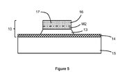
- the process for producing the microbattery comprises a step of forming a lithium-based layer 16 on the second pattern M2, after the etching of the exposed zone 13 'and the first pattern M1.
- the second material is configured so that the lithium atoms diffuse into the second pattern M2, the lithium-based layer 16 and the second pattern M2 thereby forming a second lithium-based electrode 17.
- the layer 16 is a lithium layer.
- the layer 16 may also be based on a lithium alloy.
- the lithium-based layer 16 can be made by any known means and compatible with the materials of the different layers of the microbattery, in particular the second layer 12.
- the layer 16 can be made by thermal evaporation, by spraying , or by electrodeposition.
- the lithium-based layer 16 is deposited in a localized manner on the second pattern M2.
- localized deposition means a deposit only on the second pattern M2. Therefore, it is advantageous to use a structuring step, especially an etching to obtain a structured pattern forming the electrode 17.
- a lithium-rich layer has a very high chemical instability, it is technically very difficult, if not impossible, to etch such a layer rich in lithium in order to obtain a structured pattern, as described above.
- the lithium-based layer 16 is advantageously configured to react with the second material of the pattern M2, so as to form the second electrode 17 in a lithium-rich alloy.
- a lithium-rich alloy is understood to mean an alloy comprising at least 90% lithium atoms.
- the manufacturing method according to the invention advantageously makes it possible to avoid a step of etching the lithium-rich layer 16 and to avoid any degradation of this layer by carrying out all the structuring before the deposition of the layer 16.
- the deposition technique of the lithium-based layer 16 on the second pattern M2 is configured to diffuse the lithium atoms into the second material of the second pattern.
- the deposition technique can generate a rise in temperature permitting the diffusion of the lithium atoms in the second pattern M2 so as to form a lithium-rich alloy.
- a heat treatment can be performed on the substrate during the deposition of the layer 16 by controlling the temperature of the substrate carrier. In general, it is the diffusion mechanisms that govern the formation of a lithium-second material alloy.
- a heat treatment is applied during and / or after the deposition of the lithium-based layer 16 to accelerate and favor the reaction of the material of the layer 16 with the second material of the pattern M2.
- the layer 16 and the M1 pattern undergo a heat treatment configured to diffuse the lithium atoms of the layer 16 in the first pattern M1.
- the thickness of the second layer 12 is small compared to the thickness of the lithium-based layer 16. In fact, the thickness of the layer 12 is chosen so as to allow the formation of an alloy lithium-second material, rich in lithium.
- the second layer 12 is made of silicon, and has a thickness of between 50 and 100 nm. Under these conditions, the layer 16 is lithium and its thickness is chosen greater than 1 micron.
- the method described above makes it possible to structure a solid electrolyte layer to form a microbattery.
- this type of layer it is advantageous to avoid or at least minimize the steps in which the layer is in contact with a photosensitive resin or with aqueous solutions, for example development or withdrawal.
- a solid electrolyte for example in lipon
- this type of product can modify the chemical composition of the electrolyte by oxidation and / or hydration of lithium, it can also modify the morphology of the layer of electrolyte caused by volume expansion and / or decohesion.
- lithium microbattery In a lithium microbattery, the transfer of lithium ions (Li + ) takes place at the interface between the electrolyte and the negative electrode. Thus, the quality of this interface is very critical. A chemical reactivity at this interface, which may occur during the structuring of the electrolyte layer, may cause the formation of an oxide or other phase between the electrolyte and the negative electrode layer disposed above. This phase interposed between these two active layers of the microbattery, can prevent otherwise slow the diffusion of lithium ions, thereby generating a strong charge transfer resistance within the microbattery and a deterioration of the expected electrochemical properties.
- the method for producing a microbattery according to the invention comprises an arrangement of first and second layers on the solid electrolyte prior to its structuring.
- the second layer is advantageously in contact with the solid electrolyte layer and protects it.
- the second layer is also intended to form the lithium-based negative electrode.
- the second layer disposed on the solid electrolyte prevents any contact of the solid electrolyte, in particular the electrolyte / negative electrode interface, with a photosensitive resin. Moreover, the production method minimizes the contact of the electrolyte layer with aqueous solutions.
- the first layer disposed on the second layer also preserves the interface of the second layer on which a lithium-based layer is deposited to form said negative electrode of the microbattery.
- the manufacturing method according to the invention avoids the use of mechanical masks which advantageously makes it possible to avoid shading effects and particulate contamination.
- the method makes it possible to increase the integration density of lithium microbatteries made on the same substrate, and to obtain patterns having a precise alignment while preserving the quality of the solid electrolyte.
- the deposition of an electrolyte layer through a mechanical mask does not make it possible to produce micrometric or nanometric size patterns, such as the conventional lithography techniques used in the field of microelectronics.
- the deposition through a mask also generates shading effects, negatively impacting the compactness of the microbatteries made and their electrochemical properties.
- the method described above allows structuring of several solid electrolyte units simultaneously, which reduces the time required to produce the lithium microbattery manufacturing process, in contrast to a technique for structuring the solid electrolyte by laser ablation.
- first and second layers as etching masks, facilitates the realization of the microbattery while using conventional techniques in the field of microelectronics. Thus, it is easier to incorporate or integrate a lithium microbattery on a microcomponent or on a substrate comprising other microelectronic devices or microsystems.
Landscapes
- Chemical & Material Sciences (AREA)
- Engineering & Computer Science (AREA)
- General Chemical & Material Sciences (AREA)
- Manufacturing & Machinery (AREA)
- Chemical Kinetics & Catalysis (AREA)
- Electrochemistry (AREA)
- Materials Engineering (AREA)
- Physics & Mathematics (AREA)
- Condensed Matter Physics & Semiconductors (AREA)
- General Physics & Mathematics (AREA)
- Inorganic Chemistry (AREA)
- Secondary Cells (AREA)
Applications Claiming Priority (1)
| Application Number | Priority Date | Filing Date | Title |
|---|---|---|---|
| FR1301817A FR3009136B1 (fr) | 2013-07-29 | 2013-07-29 | Procede de fabrication d'une microbatterie au lithium |
Publications (2)
| Publication Number | Publication Date |
|---|---|
| EP2833461A1 true EP2833461A1 (de) | 2015-02-04 |
| EP2833461B1 EP2833461B1 (de) | 2017-09-13 |
Family
ID=49378334
Family Applications (1)
| Application Number | Title | Priority Date | Filing Date |
|---|---|---|---|
| EP14178955.2A Active EP2833461B1 (de) | 2013-07-29 | 2014-07-29 | Herstellungsverfahren einer Lithium-Mikrobatterie |
Country Status (4)
| Country | Link |
|---|---|
| US (1) | US9373864B2 (de) |
| EP (1) | EP2833461B1 (de) |
| CN (1) | CN104393346A (de) |
| FR (1) | FR3009136B1 (de) |
Cited By (1)
| Publication number | Priority date | Publication date | Assignee | Title |
|---|---|---|---|---|
| EP3734712A1 (de) * | 2019-05-02 | 2020-11-04 | Commissariat à l'Energie Atomique et aux Energies Alternatives | Speichervorrichtung und ihr herstellungsverfahren |
Families Citing this family (4)
| Publication number | Priority date | Publication date | Assignee | Title |
|---|---|---|---|---|
| JP2016029698A (ja) * | 2014-07-22 | 2016-03-03 | デクセリアルズ株式会社 | 接続体、及び接続体の製造方法 |
| FR3050074B1 (fr) | 2016-04-07 | 2018-06-22 | Commissariat A L'energie Atomique Et Aux Energies Alternatives | Dispositif electrochimique, tel qu’une microbatterie, et son procede de realisation |
| US10749199B2 (en) | 2017-11-29 | 2020-08-18 | International Business Machines Corporation | Li1+xAlxTi2-x(PO4)3 solid-state thin film electrolyte for 3D microbattery and method of fabrication |
| GB2582177B (en) | 2019-03-14 | 2023-04-19 | Ilika Tech Limited | Method of processing layered structures |
Citations (4)
| Publication number | Priority date | Publication date | Assignee | Title |
|---|---|---|---|---|
| FR2862437A1 (fr) * | 2003-11-14 | 2005-05-20 | Commissariat Energie Atomique | Procede de fabrication d'une micro-batterie au lithium |
| FR2873854A1 (fr) * | 2004-07-30 | 2006-02-03 | Commissariat Energie Atomique | Procede de fabrication d'une electrode lithiee, electrode lithiee susceptible d'etre obtenue par ce procede et ses utilisations |
| FR2943181A1 (fr) * | 2009-03-16 | 2010-09-17 | Commissariat Energie Atomique | Microbatterie au lithium et son procede de fabrication |
| WO2012173874A2 (en) | 2011-06-17 | 2012-12-20 | Applied Materials, Inc. | Thin film battery fabrication with mask-less electrolyte deposition |
Family Cites Families (4)
| Publication number | Priority date | Publication date | Assignee | Title |
|---|---|---|---|---|
| SG173372A1 (en) * | 2006-07-18 | 2011-08-29 | Cymbet Corp | Method and apparatus for solid-state microbattery photolithographic manufacture, singulation and passivation |
| FR2936106B1 (fr) * | 2008-09-16 | 2010-10-01 | Commissariat Energie Atomique | Micro-batterie au lithium comportant une couche d'encapsulation et procede de fabrication. |
| FR2956926A1 (fr) * | 2010-03-01 | 2011-09-02 | Commissariat Energie Atomique | Microbatterie et son procede de fabrication |
| US9847326B2 (en) * | 2013-09-26 | 2017-12-19 | Infineon Technologies Ag | Electronic structure, a battery structure, and a method for manufacturing an electronic structure |
-
2013
- 2013-07-29 FR FR1301817A patent/FR3009136B1/fr not_active Expired - Fee Related
-
2014
- 2014-07-29 US US14/445,874 patent/US9373864B2/en active Active
- 2014-07-29 EP EP14178955.2A patent/EP2833461B1/de active Active
- 2014-07-29 CN CN201410539657.5A patent/CN104393346A/zh active Pending
Patent Citations (4)
| Publication number | Priority date | Publication date | Assignee | Title |
|---|---|---|---|---|
| FR2862437A1 (fr) * | 2003-11-14 | 2005-05-20 | Commissariat Energie Atomique | Procede de fabrication d'une micro-batterie au lithium |
| FR2873854A1 (fr) * | 2004-07-30 | 2006-02-03 | Commissariat Energie Atomique | Procede de fabrication d'une electrode lithiee, electrode lithiee susceptible d'etre obtenue par ce procede et ses utilisations |
| FR2943181A1 (fr) * | 2009-03-16 | 2010-09-17 | Commissariat Energie Atomique | Microbatterie au lithium et son procede de fabrication |
| WO2012173874A2 (en) | 2011-06-17 | 2012-12-20 | Applied Materials, Inc. | Thin film battery fabrication with mask-less electrolyte deposition |
Cited By (3)
| Publication number | Priority date | Publication date | Assignee | Title |
|---|---|---|---|---|
| EP3734712A1 (de) * | 2019-05-02 | 2020-11-04 | Commissariat à l'Energie Atomique et aux Energies Alternatives | Speichervorrichtung und ihr herstellungsverfahren |
| FR3095721A1 (fr) * | 2019-05-02 | 2020-11-06 | Commissariat A L'energie Atomique Et Aux Energies Alternatives | Dispositif de stockage et procédé de fabrication |
| US11362314B2 (en) | 2019-05-02 | 2022-06-14 | Commissariat A L'energie Atomique Et Aux Energies Alternatives | Storage device and manufacturing method |
Also Published As
| Publication number | Publication date |
|---|---|
| CN104393346A (zh) | 2015-03-04 |
| US20150027979A1 (en) | 2015-01-29 |
| FR3009136A1 (fr) | 2015-01-30 |
| FR3009136B1 (fr) | 2017-10-27 |
| EP2833461B1 (de) | 2017-09-13 |
| US9373864B2 (en) | 2016-06-21 |
Similar Documents
| Publication | Publication Date | Title |
|---|---|---|
| EP2409352B1 (de) | Lithium-Mikrobatterie und Herstellungsverfahren dafür | |
| JP6283433B2 (ja) | 薄膜電池のマスクレス製造 | |
| EP2432065B1 (de) | Verfahren zur Strukturierung einer Polymerschicht und Verfahren zur Einkapselung einer Mikrobatterie | |
| EP1683217B1 (de) | Verfahren zur herstellung einer lithium-mikrobatterie | |
| EP2833461B1 (de) | Herstellungsverfahren einer Lithium-Mikrobatterie | |
| CA2848580C (fr) | Procede de preparation d'electrode a partir d'un materiau poreux, electrode ainsi obtenue et systeme electrochimique correspondant | |
| TWI618278B (zh) | 垂直薄膜電池之無遮罩製造 | |
| FR2936106A1 (fr) | Micro-batterie au lithium comportant une couche d'encapsulation et procede de fabrication. | |
| FR2950741A1 (fr) | Procede de formation d'une batterie lithium-ion verticale en couches minces | |
| FR2994338A1 (fr) | Procede de formation d'une batterie de type lithium-ion | |
| EP3047530B1 (de) | Verfahren zur herstellung einer lithiummikrobatterie und lithiummikrobatterie | |
| EP3260511B1 (de) | Reversibles klebeverfahren zwischen zwei elementen | |
| EP3528320B1 (de) | Herstellungsverfahren einer positiven elektrode für feste lithium-mikrobatterie | |
| FR3076061B1 (fr) | Realisation d'un collecteur de dispositif microelectronique | |
| EP3503143B1 (de) | Herstellung eines kollektors für eine mikroelektronische vorrichtung | |
| EP3734712B1 (de) | Speichervorrichtung und ihr herstellungsverfahren | |
| FR3161308A1 (fr) | Micro-batterie | |
| WO2012176527A1 (ja) | 結晶太陽電池セルおよび結晶太陽電池セルの製造方法 |
Legal Events
| Date | Code | Title | Description |
|---|---|---|---|
| 17P | Request for examination filed |
Effective date: 20140729 |
|
| AK | Designated contracting states |
Kind code of ref document: A1 Designated state(s): AL AT BE BG CH CY CZ DE DK EE ES FI FR GB GR HR HU IE IS IT LI LT LU LV MC MK MT NL NO PL PT RO RS SE SI SK SM TR |
|
| AX | Request for extension of the european patent |
Extension state: BA ME |
|
| PUAI | Public reference made under article 153(3) epc to a published international application that has entered the european phase |
Free format text: ORIGINAL CODE: 0009012 |
|
| R17P | Request for examination filed (corrected) |
Effective date: 20150618 |
|
| RBV | Designated contracting states (corrected) |
Designated state(s): AL AT BE BG CH CY CZ DE DK EE ES FI FR GB GR HR HU IE IS IT LI LT LU LV MC MK MT NL NO PL PT RO RS SE SI SK SM TR |
|
| REG | Reference to a national code |
Ref country code: DE Ref legal event code: R079 Ref document number: 602014014470 Country of ref document: DE Free format text: PREVIOUS MAIN CLASS: H01M0010040000 Ipc: H01M0010052000 |
|
| RIC1 | Information provided on ipc code assigned before grant |
Ipc: H01M 10/0585 20100101ALI20170222BHEP Ipc: H01M 4/1395 20100101ALI20170222BHEP Ipc: H01M 6/40 20060101ALI20170222BHEP Ipc: H01M 10/052 20100101AFI20170222BHEP Ipc: H01M 6/18 20060101ALI20170222BHEP Ipc: H01M 10/0562 20100101ALI20170222BHEP |
|
| GRAP | Despatch of communication of intention to grant a patent |
Free format text: ORIGINAL CODE: EPIDOSNIGR1 |
|
| STAA | Information on the status of an ep patent application or granted ep patent |
Free format text: STATUS: GRANT OF PATENT IS INTENDED |
|
| INTG | Intention to grant announced |
Effective date: 20170411 |
|
| GRAS | Grant fee paid |
Free format text: ORIGINAL CODE: EPIDOSNIGR3 |
|
| GRAA | (expected) grant |
Free format text: ORIGINAL CODE: 0009210 |
|
| STAA | Information on the status of an ep patent application or granted ep patent |
Free format text: STATUS: THE PATENT HAS BEEN GRANTED |
|
| AK | Designated contracting states |
Kind code of ref document: B1 Designated state(s): AL AT BE BG CH CY CZ DE DK EE ES FI FR GB GR HR HU IE IS IT LI LT LU LV MC MK MT NL NO PL PT RO RS SE SI SK SM TR |
|
| REG | Reference to a national code |
Ref country code: GB Ref legal event code: FG4D Free format text: NOT ENGLISH |
|
| REG | Reference to a national code |
Ref country code: CH Ref legal event code: EP |
|
| REG | Reference to a national code |
Ref country code: IE Ref legal event code: FG4D Free format text: LANGUAGE OF EP DOCUMENT: FRENCH |
|
| REG | Reference to a national code |
Ref country code: AT Ref legal event code: REF Ref document number: 928972 Country of ref document: AT Kind code of ref document: T Effective date: 20171015 |
|
| REG | Reference to a national code |
Ref country code: DE Ref legal event code: R096 Ref document number: 602014014470 Country of ref document: DE |
|
| REG | Reference to a national code |
Ref country code: NL Ref legal event code: MP Effective date: 20170913 |
|
| REG | Reference to a national code |
Ref country code: LT Ref legal event code: MG4D |
|
| PG25 | Lapsed in a contracting state [announced via postgrant information from national office to epo] |
Ref country code: LT Free format text: LAPSE BECAUSE OF FAILURE TO SUBMIT A TRANSLATION OF THE DESCRIPTION OR TO PAY THE FEE WITHIN THE PRESCRIBED TIME-LIMIT Effective date: 20170913 Ref country code: SE Free format text: LAPSE BECAUSE OF FAILURE TO SUBMIT A TRANSLATION OF THE DESCRIPTION OR TO PAY THE FEE WITHIN THE PRESCRIBED TIME-LIMIT Effective date: 20170913 Ref country code: FI Free format text: LAPSE BECAUSE OF FAILURE TO SUBMIT A TRANSLATION OF THE DESCRIPTION OR TO PAY THE FEE WITHIN THE PRESCRIBED TIME-LIMIT Effective date: 20170913 Ref country code: NO Free format text: LAPSE BECAUSE OF FAILURE TO SUBMIT A TRANSLATION OF THE DESCRIPTION OR TO PAY THE FEE WITHIN THE PRESCRIBED TIME-LIMIT Effective date: 20171213 Ref country code: HR Free format text: LAPSE BECAUSE OF FAILURE TO SUBMIT A TRANSLATION OF THE DESCRIPTION OR TO PAY THE FEE WITHIN THE PRESCRIBED TIME-LIMIT Effective date: 20170913 |
|
| REG | Reference to a national code |
Ref country code: AT Ref legal event code: MK05 Ref document number: 928972 Country of ref document: AT Kind code of ref document: T Effective date: 20170913 |
|
| PG25 | Lapsed in a contracting state [announced via postgrant information from national office to epo] |
Ref country code: BG Free format text: LAPSE BECAUSE OF FAILURE TO SUBMIT A TRANSLATION OF THE DESCRIPTION OR TO PAY THE FEE WITHIN THE PRESCRIBED TIME-LIMIT Effective date: 20171213 Ref country code: GR Free format text: LAPSE BECAUSE OF FAILURE TO SUBMIT A TRANSLATION OF THE DESCRIPTION OR TO PAY THE FEE WITHIN THE PRESCRIBED TIME-LIMIT Effective date: 20171214 Ref country code: ES Free format text: LAPSE BECAUSE OF FAILURE TO SUBMIT A TRANSLATION OF THE DESCRIPTION OR TO PAY THE FEE WITHIN THE PRESCRIBED TIME-LIMIT Effective date: 20170913 Ref country code: RS Free format text: LAPSE BECAUSE OF FAILURE TO SUBMIT A TRANSLATION OF THE DESCRIPTION OR TO PAY THE FEE WITHIN THE PRESCRIBED TIME-LIMIT Effective date: 20170913 Ref country code: LV Free format text: LAPSE BECAUSE OF FAILURE TO SUBMIT A TRANSLATION OF THE DESCRIPTION OR TO PAY THE FEE WITHIN THE PRESCRIBED TIME-LIMIT Effective date: 20170913 |
|
| PG25 | Lapsed in a contracting state [announced via postgrant information from national office to epo] |
Ref country code: NL Free format text: LAPSE BECAUSE OF FAILURE TO SUBMIT A TRANSLATION OF THE DESCRIPTION OR TO PAY THE FEE WITHIN THE PRESCRIBED TIME-LIMIT Effective date: 20170913 |
|
| PG25 | Lapsed in a contracting state [announced via postgrant information from national office to epo] |
Ref country code: RO Free format text: LAPSE BECAUSE OF FAILURE TO SUBMIT A TRANSLATION OF THE DESCRIPTION OR TO PAY THE FEE WITHIN THE PRESCRIBED TIME-LIMIT Effective date: 20170913 Ref country code: CZ Free format text: LAPSE BECAUSE OF FAILURE TO SUBMIT A TRANSLATION OF THE DESCRIPTION OR TO PAY THE FEE WITHIN THE PRESCRIBED TIME-LIMIT Effective date: 20170913 Ref country code: PL Free format text: LAPSE BECAUSE OF FAILURE TO SUBMIT A TRANSLATION OF THE DESCRIPTION OR TO PAY THE FEE WITHIN THE PRESCRIBED TIME-LIMIT Effective date: 20170913 |
|
| PG25 | Lapsed in a contracting state [announced via postgrant information from national office to epo] |
Ref country code: SM Free format text: LAPSE BECAUSE OF FAILURE TO SUBMIT A TRANSLATION OF THE DESCRIPTION OR TO PAY THE FEE WITHIN THE PRESCRIBED TIME-LIMIT Effective date: 20170913 Ref country code: SK Free format text: LAPSE BECAUSE OF FAILURE TO SUBMIT A TRANSLATION OF THE DESCRIPTION OR TO PAY THE FEE WITHIN THE PRESCRIBED TIME-LIMIT Effective date: 20170913 Ref country code: AT Free format text: LAPSE BECAUSE OF FAILURE TO SUBMIT A TRANSLATION OF THE DESCRIPTION OR TO PAY THE FEE WITHIN THE PRESCRIBED TIME-LIMIT Effective date: 20170913 Ref country code: EE Free format text: LAPSE BECAUSE OF FAILURE TO SUBMIT A TRANSLATION OF THE DESCRIPTION OR TO PAY THE FEE WITHIN THE PRESCRIBED TIME-LIMIT Effective date: 20170913 Ref country code: IS Free format text: LAPSE BECAUSE OF FAILURE TO SUBMIT A TRANSLATION OF THE DESCRIPTION OR TO PAY THE FEE WITHIN THE PRESCRIBED TIME-LIMIT Effective date: 20180113 Ref country code: IT Free format text: LAPSE BECAUSE OF FAILURE TO SUBMIT A TRANSLATION OF THE DESCRIPTION OR TO PAY THE FEE WITHIN THE PRESCRIBED TIME-LIMIT Effective date: 20170913 |
|
| REG | Reference to a national code |
Ref country code: DE Ref legal event code: R097 Ref document number: 602014014470 Country of ref document: DE |
|
| PLBE | No opposition filed within time limit |
Free format text: ORIGINAL CODE: 0009261 |
|
| STAA | Information on the status of an ep patent application or granted ep patent |
Free format text: STATUS: NO OPPOSITION FILED WITHIN TIME LIMIT |
|
| REG | Reference to a national code |
Ref country code: FR Ref legal event code: PLFP Year of fee payment: 5 |
|
| PG25 | Lapsed in a contracting state [announced via postgrant information from national office to epo] |
Ref country code: DK Free format text: LAPSE BECAUSE OF FAILURE TO SUBMIT A TRANSLATION OF THE DESCRIPTION OR TO PAY THE FEE WITHIN THE PRESCRIBED TIME-LIMIT Effective date: 20170913 |
|
| 26N | No opposition filed |
Effective date: 20180614 |
|
| PG25 | Lapsed in a contracting state [announced via postgrant information from national office to epo] |
Ref country code: MT Free format text: LAPSE BECAUSE OF FAILURE TO SUBMIT A TRANSLATION OF THE DESCRIPTION OR TO PAY THE FEE WITHIN THE PRESCRIBED TIME-LIMIT Effective date: 20170913 |
|
| PG25 | Lapsed in a contracting state [announced via postgrant information from national office to epo] |
Ref country code: SI Free format text: LAPSE BECAUSE OF FAILURE TO SUBMIT A TRANSLATION OF THE DESCRIPTION OR TO PAY THE FEE WITHIN THE PRESCRIBED TIME-LIMIT Effective date: 20170913 |
|
| REG | Reference to a national code |
Ref country code: CH Ref legal event code: PL |
|
| PG25 | Lapsed in a contracting state [announced via postgrant information from national office to epo] |
Ref country code: LU Free format text: LAPSE BECAUSE OF NON-PAYMENT OF DUE FEES Effective date: 20180729 Ref country code: MC Free format text: LAPSE BECAUSE OF FAILURE TO SUBMIT A TRANSLATION OF THE DESCRIPTION OR TO PAY THE FEE WITHIN THE PRESCRIBED TIME-LIMIT Effective date: 20170913 |
|
| REG | Reference to a national code |
Ref country code: BE Ref legal event code: MM Effective date: 20180731 |
|
| PG25 | Lapsed in a contracting state [announced via postgrant information from national office to epo] |
Ref country code: LI Free format text: LAPSE BECAUSE OF NON-PAYMENT OF DUE FEES Effective date: 20180731 Ref country code: CH Free format text: LAPSE BECAUSE OF NON-PAYMENT OF DUE FEES Effective date: 20180731 |
|
| REG | Reference to a national code |
Ref country code: IE Ref legal event code: MM4A |
|
| PG25 | Lapsed in a contracting state [announced via postgrant information from national office to epo] |
Ref country code: BE Free format text: LAPSE BECAUSE OF NON-PAYMENT OF DUE FEES Effective date: 20180731 |
|
| PG25 | Lapsed in a contracting state [announced via postgrant information from national office to epo] |
Ref country code: IE Free format text: LAPSE BECAUSE OF NON-PAYMENT OF DUE FEES Effective date: 20180729 |
|
| PG25 | Lapsed in a contracting state [announced via postgrant information from national office to epo] |
Ref country code: TR Free format text: LAPSE BECAUSE OF FAILURE TO SUBMIT A TRANSLATION OF THE DESCRIPTION OR TO PAY THE FEE WITHIN THE PRESCRIBED TIME-LIMIT Effective date: 20170913 |
|
| PG25 | Lapsed in a contracting state [announced via postgrant information from national office to epo] |
Ref country code: HU Free format text: LAPSE BECAUSE OF FAILURE TO SUBMIT A TRANSLATION OF THE DESCRIPTION OR TO PAY THE FEE WITHIN THE PRESCRIBED TIME-LIMIT; INVALID AB INITIO Effective date: 20140729 Ref country code: PT Free format text: LAPSE BECAUSE OF FAILURE TO SUBMIT A TRANSLATION OF THE DESCRIPTION OR TO PAY THE FEE WITHIN THE PRESCRIBED TIME-LIMIT Effective date: 20170913 |
|
| PG25 | Lapsed in a contracting state [announced via postgrant information from national office to epo] |
Ref country code: CY Free format text: LAPSE BECAUSE OF FAILURE TO SUBMIT A TRANSLATION OF THE DESCRIPTION OR TO PAY THE FEE WITHIN THE PRESCRIBED TIME-LIMIT Effective date: 20170913 Ref country code: MK Free format text: LAPSE BECAUSE OF NON-PAYMENT OF DUE FEES Effective date: 20170913 |
|
| PG25 | Lapsed in a contracting state [announced via postgrant information from national office to epo] |
Ref country code: AL Free format text: LAPSE BECAUSE OF FAILURE TO SUBMIT A TRANSLATION OF THE DESCRIPTION OR TO PAY THE FEE WITHIN THE PRESCRIBED TIME-LIMIT Effective date: 20170913 |
|
| PGFP | Annual fee paid to national office [announced via postgrant information from national office to epo] |
Ref country code: DE Payment date: 20250722 Year of fee payment: 12 |
|
| PGFP | Annual fee paid to national office [announced via postgrant information from national office to epo] |
Ref country code: GB Payment date: 20250724 Year of fee payment: 12 |
|
| PGFP | Annual fee paid to national office [announced via postgrant information from national office to epo] |
Ref country code: FR Payment date: 20250722 Year of fee payment: 12 |