EP2835749A1 - Procédé d'obtention d'un modèle de circuit équivalent d'un condensateur - Google Patents
Procédé d'obtention d'un modèle de circuit équivalent d'un condensateur Download PDFInfo
- Publication number
- EP2835749A1 EP2835749A1 EP13772567.7A EP13772567A EP2835749A1 EP 2835749 A1 EP2835749 A1 EP 2835749A1 EP 13772567 A EP13772567 A EP 13772567A EP 2835749 A1 EP2835749 A1 EP 2835749A1
- Authority
- EP
- European Patent Office
- Prior art keywords
- capacitor
- circuit
- capacitive
- equivalent circuit
- inductive
- Prior art date
- Legal status (The legal status is an assumption and is not a legal conclusion. Google has not performed a legal analysis and makes no representation as to the accuracy of the status listed.)
- Granted
Links
Images


Classifications
-
- G—PHYSICS
- G06—COMPUTING OR CALCULATING; COUNTING
- G06F—ELECTRIC DIGITAL DATA PROCESSING
- G06F30/00—Computer-aided design [CAD]
-
- G—PHYSICS
- G06—COMPUTING OR CALCULATING; COUNTING
- G06F—ELECTRIC DIGITAL DATA PROCESSING
- G06F30/00—Computer-aided design [CAD]
- G06F30/30—Circuit design
- G06F30/39—Circuit design at the physical level
- G06F30/398—Design verification or optimisation, e.g. using design rule check [DRC], layout versus schematics [LVS] or finite element methods [FEM]
-
- G—PHYSICS
- G06—COMPUTING OR CALCULATING; COUNTING
- G06F—ELECTRIC DIGITAL DATA PROCESSING
- G06F30/00—Computer-aided design [CAD]
- G06F30/30—Circuit design
- G06F30/36—Circuit design at the analogue level
- G06F30/367—Design verification, e.g. using simulation, simulation program with integrated circuit emphasis [SPICE], direct methods or relaxation methods
-
- H—ELECTRICITY
- H01—ELECTRIC ELEMENTS
- H01G—CAPACITORS; CAPACITORS, RECTIFIERS, DETECTORS, SWITCHING DEVICES, LIGHT-SENSITIVE OR TEMPERATURE-SENSITIVE DEVICES OF THE ELECTROLYTIC TYPE
- H01G4/00—Fixed capacitors; Processes of their manufacture
- H01G4/002—Details
- H01G4/018—Dielectrics
- H01G4/06—Solid dielectrics
- H01G4/08—Inorganic dielectrics
- H01G4/12—Ceramic dielectrics
-
- H—ELECTRICITY
- H01—ELECTRIC ELEMENTS
- H01G—CAPACITORS; CAPACITORS, RECTIFIERS, DETECTORS, SWITCHING DEVICES, LIGHT-SENSITIVE OR TEMPERATURE-SENSITIVE DEVICES OF THE ELECTROLYTIC TYPE
- H01G4/00—Fixed capacitors; Processes of their manufacture
- H01G4/002—Details
- H01G4/255—Means for correcting the capacitance value
-
- H—ELECTRICITY
- H01—ELECTRIC ELEMENTS
- H01G—CAPACITORS; CAPACITORS, RECTIFIERS, DETECTORS, SWITCHING DEVICES, LIGHT-SENSITIVE OR TEMPERATURE-SENSITIVE DEVICES OF THE ELECTROLYTIC TYPE
- H01G4/00—Fixed capacitors; Processes of their manufacture
- H01G4/30—Stacked capacitors
Definitions
- the present invention relates to methods for deriving equivalent circuit models of capacitors that are formed by a resistive element, a capacitive element, and an inductive element serving as elements.
- Circuit simulators such as SPICE (Simulation Program with Integrated Circuit) are used for circuit simulations, and some circuit simulators are available for use on websites of electronic component manufacturers. Users access the websites of the electronic component manufacturers from terminals, such as a personal computer, through the Internet and use the circuit simulators.
- Patent Document 1 Disclosed in Patent Document 1, for example, is an existing method for deriving an equivalent circuit model of a capacitor.
- this method for deriving an equivalent circuit model given frequency characteristics of a capacitor are inputted in a first step, and, in a second step, one of an RC circuit, an RL circuit, and an RCL circuit is formed as an equivalent circuit model, or a circuit that can be simulated in a time domain, by using a resistance (R), a capacitance (C), and an inductance (L) that are not dependent on the frequency.
- R resistance
- C capacitance
- L inductance
- Patent Document 1 through the configuration described above, such an equivalent circuit model of a capacitor, of which an impedance is indicated in a frequency domain, that can be simulated in a time domain is derived, and the electrical characteristics of the capacitor in the frequency domain or in the time domain are predicted through a circuit simulation.
- Patent Document 1 Japanese Unexamined Patent Application Publication No. 2002-259482
- the present invention has been made to solve such a Problem, and in a method for deriving an equivalent circuit model of a capacitor that is formed by a resistive element, a capacitive element, and an inductive element serving as elements, a rate of change in a characteristic value of the element of which the characteristic value changes as a direct current voltage is applied to the capacitor is expressed as a dimensionless coefficient on the basis of a rate of change in the characteristics of the capacitor attributable to a material of the capacitor; the characteristic value of the element, of which the characteristic value changes in response to the direct current voltage being applied to the capacitor, held while the direct current voltage is not applied is multiplied by the dimensionless coefficient; and the characteristic value of the element is corrected to a value in accordance with the direct current voltage applied to the capacitor.
- the characteristic value of an element namely, a resistive element, a capacitive element, or an inductive element which forms the equivalent circuit model of the capacitor and of which the characteristic value changes in response to the direct current voltage being applied to the capacitor, held while the direct current voltage is not applied by the dimensionless coefficient, the characteristic value of the element forming the equivalent circuit model of the capacitor can be corrected to a value in accordance with the direct current voltage applied to the capacitor.
- an equivalent circuit model does not need to be derived for each value of the direct current voltage superimposed and applied to the capacitor, and the equivalent circuit model provided with characteristics in accordance with the direct current voltage superimposed and applied to the capacitor can be derived with high accuracy and with ease.
- the equivalent circuit model is formed by a resonant circuit serving as a circuit element, and the resonant circuit is formed by a resistive element, a capacitive element, and an inductive element.
- the characteristics of the capacitor change around the self resonant frequency or the secondary resonant frequency exceeding the self resonant frequency.
- the equivalent circuit model is formed by the resonant circuit serving as a circuit element, and the resonant circuit is formed by a resistive element, a capacitive element, and an inductive element.
- the change in the characteristics can be simulated accurately.
- the equivalent circuit model is formed by one of a main resonant circuit, a secondary resonant circuit, a capacitive circuit, and an inductive circuit.
- the main resonant circuit is formed by connecting a resistive element, a capacitive element, and an inductive element in series;
- the secondary resonant circuit is formed by connecting a resistive element, a capacitive element, and an inductive element in parallel;
- the capacitive circuit is formed by connecting a resistive element and a capacitive element in parallel;
- the inductive circuit is is formed by connecting a resistive element and an inductive element in parallel.
- the equivalent circuit model is formed by connecting some of the main resonant circuit, the secondary resonant circuit, the capacitive circuit, and the inductive circuit in series.
- the equivalent circuit model is formed so as to include the main resonant circuit in which a resistive element, a capacitive element, and an inductive element are connected in series, in accordance with the material of the capacitor, the characteristics at a frequency around the self resonant frequency are corrected appropriately. Additionally, as the equivalent circuit model is formed so as to include the capacitive circuit in which a resistive element and a capacitive element are connected in parallel, in accordance with the material of the capacitor, the characteristics at a frequency toward a lower frequency side of the self resonant frequency are corrected appropriately.
- the equivalent circuit model is formed so as to include the secondary resonant circuit in which a resistive element, a capacitive element, and an inductive element are connected in parallel, in accordance with the material of the capacitor, the characteristics at a frequency around the secondary resonant frequency exceeding the self resonant frequency are corrected appropriately.
- the equivalent circuit model is formed so as to include the inductive circuit in which a resistive element and an inductive element are connected in parallel, in accordance with the material of the capacitor, the characteristics at a frequency toward a higher frequency side of the self resonant frequency are corrected appropriately.
- the equivalent circuit model is formed by one of a main resonant circuit, a secondary resonant circuit, a capacitive circuit, and an inductive circuit.
- the main resonant circuit is formed by connecting a resistive element, a capacitive element, and an inductive element in parallel;
- the secondary resonant circuit is formed by connecting a resistive element, a capacitive element, and an inductive element in series;
- the capacitive circuit is formed by connecting a resistive element and a capacitive element in series;
- the inductive circuit is formed by connecting a resistive element and an inductive element in series.
- the equivalent circuit model is formed by connecting some of the main resonant circuit, the secondary resonant circuit, the capacitive circuit, and the inductive circuit in parallel.
- the equivalent circuit model is formed so as to include the main resonant circuit in which a resistive element, a capacitive element, and an inductive element are connected in parallel, in accordance with the material of the capacitor the characteristics at a frequency around the self resonant frequency are corrected appropriately. Additionally, as the equivalent circuit model is formed so as to include the capacitive circuit in which a resistive element and a capacitive element are connected in series, in accordance with the material of the capacitor, the characteristics at a frequency toward a lower frequency side of the self resonant frequency are corrected appropriately.
- the equivalent circuit model is formed so as to include the secondary resonant circuit in which a resistive element, a capacitive element, and an inductive element are connected in series, in accordance with the material of the capacitor the characteristics at a frequency around the secondary resonant frequency exceeding the self resonant frequency are corrected appropriately.
- the equivalent circuit model is formed so as to include the inductive circuit in which a resistive element and an inductive element are connected in series, in accordance with the material of the capacitor the characteristics at a frequency toward a higher frequency side of the self resonant frequency are corrected appropriately.
- the dimensionless coefficient is expressed for the capacitive element or the resistive element, of which the characteristic value changes in response to the direct current voltage being applied to the capacitor, on the basis of one or both of a rate of change in the capacitance and a rate of change in the dielectric loss of the capacitor measured by applying the direct current voltage to the capacitor, and the correction is carried out by multiplying a capacitance value of the capacitive element, of which the capacitance value changes in response to the direct current voltage being applied to the capacitor, held while the direct current voltage is not applied or a resistance value of the resistive element, of which the resistance value changes in response to the direct current voltage being applied to the capacitor, held while the direct current voltage is not applied by the dimensionless coefficient.
- the dimensionless coefficient is expressed for the capacitive element or the resistive element, of which the characteristic value changes in response to the direct current voltage being applied to the capacitor, and the characteristic value of the capacitance value or the resistance value is corrected appropriately to a value in accordance with the direct current voltage superimposed and applied to the capacitor by multiplying the characteristic value held while the direct current voltage is not applied to the capacitor by the dimensionless coefficient.
- the rate of change in the characteristic value of the element is expressed as an approximate function of the direct current voltage applied to the capacitor.
- the characteristic value of an element namely, a resistive element, a capacitive element, or an inductive element forming the equivalent circuit model of the capacitor has its rate of change expressed as an approximate function of the direct current voltage applied to the capacitor, and thus values obtained discretely through the measurement are complemented and can be grasped continuously from the characteristic value held while the direct current voltage is not applied. Therefore, in each of the equivalent circuit models derived in accordance with the direct current voltage superimposed and applied to the capacitor, the continuity or the relationship with the equivalent circuit model obtained when the direct current voltage is not applied becomes clear, and thus the change in the characteristics arising while the direct current voltage is applied to the capacitor up to the rated voltage thereof can be foreseen continuously.
- the approximate function is expressed within a direct current voltage range that ranges from a rated voltage of the capacitor or lower to zero or higher, and a function value always takes a positive value and becomes 1 when the direct current voltage applied to the capacitor is zero.
- the rate of change in the characteristic value of the element forming the equivalent circuit model of the capacitor is expressed through an approximate function in accordance with the actual use of the capacitor, and thus an appropriate circuit simulation can be carried out in accordance with the actual use.
- a computer program that causes one of the above-described methods for deriving an equivalent circuit model of a capacitor to function is formed, and the computer program includes a first step of inputting a type of the capacitor, a second step of inputting a value of a direct current voltage to be applied to the capacitor, and a third step of multiplying a characteristic value of the element forming the equivalent circuit model of the capacitor of the type inputted in the first step held while the direct current voltage is not applied by a dimensionless coefficient prepared in advance for the capacitor of the type inputted in the first step and correcting the characteristic value of the element to a value in accordance with the direct current voltage inputted in the second step.
- the characteristic value of the element forming the equivalent circuit model of the capacitor of the inputted type is automatically corrected through the computer program to a value in accordance with the inputted value of the direct current voltage as the characteristic value held while the direct current voltage is not applied is multiplied by the dimensionless coefficient prepared in advance for the capacitor of the inputted type.
- a user of the deriving method can carry out, with high accuracy and with ease, an appropriate circuit simulation only by inputting the type of the capacitor to be simulated and the value of the direct current voltage to be applied to the capacitor to the computer program.
- an appropriate circuit simulation for an electronic circuit that includes the capacitor with high accuracy and with ease.
- a method for using the computer program includes accessing a server provided with the computer program though the Internet, and using the computer program from a terminal connected to the Internet.
- the user can use the computer program with ease by accessing the server provided with the computer program from a terminal connected to the Internet. Accordingly, the method for deriving the equivalent circuit model of the capacitor according to the present invention can be provided to a large number of users.
- an equivalent circuit model having characteristics in accordance with a direct current voltage to be superimposed and applied to a capacitor can be derived with high accuracy and with ease.
- the continuity or the relationship with the equivalent circuit model obtained when the direct current voltage is not applied becomes clear, and thus the change in the characteristics arising while the direct current voltage is applied to the capacitor up to the rated voltage thereof can be foreseen continuously.
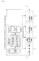
- a laminated ceramic capacitor 1 is a surface mounted chip capacitor, and includes a dielectric 2 that is formed by stacking ceramic layers and has a substantially a rectangular parallelepiped shape and a pair of electrode terminals 3a and 3b disposed at respective end portions of the dielectric 2.
- a plurality of internal electrodes forming the capacitor are disposed facing one another inside the dielectric 2.
- the pair of electrode terminals 3a and 3b is connected to each of the internal electrodes that face one another.
- Such a laminated ceramic capacitor 1 is formed so as to include a resistance component, a capacitance component, and an inductance component.
- the laminated ceramic capacitor 1 is formed by a resistive element R, a capacitive element C, and an inductive element L serving as elements, and includes a main resonant circuit 11, an secondary resonant circuit 12, a capacitive circuit 13, and an inductive circuit 14 that are connected in series.
- the main resonant circuit 11 is formed by connecting a resistive element R, a capacitive element C, and an inductive element L in series;
- the secondary resonant circuit 12 is formed by connecting a resistive element R, a capacitive element C, and an inductive element L in parallel;
- the capacitive circuit 13 is formed by connecting a resistive element R and a capacitive element C in parallel;
- the inductive circuit 14 is formed by connecting a resistive element R and an inductive element L in parallel.
- a DC bias voltage v2 is superimposed on an alternating current voltage v1, and the resulting voltage is applied across the electrode terminals 3a and 3b.
- a rate of change in a characteristic value of an element namely, a resistive element R, a capacitive element C, or an inductive element L, that changes as the DC bias voltage v2 is applied to the capacitor 1 is expressed as a dimensionless coefficient 15 on the basis of a rate of change in the characteristics of the capacitor 1 attributable to the material of the dielectric 2 in the capacitor 1.
- the characteristic value of the aforementioned element forming the main resonant circuit 11, the secondary resonant circuit 12, the capacitive circuit 13, or the inductive circuit 14 is corrected to a value in accordance with the DC bias voltage v2 applied to the capacitor 1.
- the dimensionless coefficient 15 is expressed for a capacitive element C or a resistive element R, of which the characteristic value changes in response to the DC bias voltage v2 being applied to the capacitor 1, on the basis of one or both of a rate of change in the capacitance Kc or a rate of change in the dielectric loss Kd of the capacitor 1, which is measured by applying the DC bias voltage v2 to the capacitor 1.
- the application rule 16 is defined as a rule in which the characteristic value of the aforementioned element, of which the characteristic value changes in response to the DC bias voltage v2 being applied to the capacitor 1, held while the DC bias voltage v2 is not applied is multiplied by the dimensionless coefficient 15.
- the characteristic value is corrected by multiplying the capacitance value of the capacitive element C, of which the capacitance value changes in accordance with the DC bias voltage v2, held while a direct current voltage is not applied and the resistance value of the resistive element R, of which the resistance value changes in accordance with the DC bias voltage v2, held while a direct current voltage is not applied by the dimensionless coefficient 15 in accordance with the application rule 16.
- This multiplication by the dimensionless coefficient 15 according to the application rule 16 is implemented by multiplying or dividing one of or a combination of both of the rate of change in the capacitance Kc and the rate of change in the dielectric loss Kd by the dimensionless coefficient 15, which will be described later.
- Fig. 3 is a circuit diagram illustrating a specific example of the equivalent circuit model of the capacitor 1.
- a main resonant circuit 11A, a capacitive circuit 13A, a first secondary resonant circuit 12A, an inductive circuit 14A, and a second secondary resonant circuit 12B are connected in series to form an equivalent circuit model.
- the main resonant circuit 11A is formed by a resistive element R1, a capacitive element C1, and an inductive element L1 that are connected in series.
- the resistance value of the resistive element R1 is 2.46 ⁇ 10 0 [m ⁇ ]; the capacitance value of the capacitive element C1 is 8.14 ⁇ 10 0 [ ⁇ F]; and the inductance of the inductive element L1 is 1.17 ⁇ 10 2 [pH].
- the change in the characteristics of the resistive element R1 and the inductive element L1 of the main resonant circuit 11A resulting as the DC bias voltage v2 is applied is attributable to the metal material of the internal electrodes and the electrode terminals 3a and 3b of the capacitor 1 or to the structure or the like of the capacitor 1 and is not attributable to the material of the dielectric 2. Meanwhile, the change in the characteristics of the capacitive element C1 resulting as the DC bias voltage v2 is applied is attributable to the material of the dielectric 2. Therefore, in the main resonant circuit 11A, the characteristics of the capacitive element C1 need to be corrected in accordance with the applied voltage of the DC bias voltage v2.
- an application rule I is employed in which the capacitance value of the capacitive element C1 is multiplied by the rate of change in the capacitance Kc.
- the dimensionless coefficient 15 is set to the rate of change in the capacitance Kc.
- the capacitive circuit 13A is formed by five parallel circuits 13A1, 13A2, 13A3, 13A4, and 13A5 that are connected in series, and the parallel circuits 13A1, 13A2, 13A3, 13A4, and 13A5 are formed by respective resistive elements R2, R3, R4, R5, and R6 and respective capacitive elements C2, C3, C4, C5, and C6.
- the resistance values of the resistive elements R2, R3, R4, R5, and R6 are, respectively, 5.81 ⁇ 10 3 , 5.58 ⁇ 10 2 , 6.43 ⁇ 10 1 , 7.07 ⁇ 10 0 , and 1.74 ⁇ 10 0 [m ⁇ ]; and the capacitance values of the capacitive elements C2, C3, C4, C5, and C6 are, respectively, 5.50 ⁇ 10 2 , 7.16 ⁇ 10 2 , 8.86 ⁇ 10 2 , 1.40 ⁇ 10 3 , and 1.25 ⁇ 10 3 [ ⁇ F].
- each of the resistive elements R2 to R5 and the capacitive elements C2 to C5 forming the capacitive circuit 13A change as the DC bias voltage v2 is applied, and such a change is attributable to the material of the dielectric 2. Therefore, in the capacitive circuit 13A, the characteristics of all of the elements, namely, the resistive elements R2 to R5 and the capacitive elements C2 to C5 need to be corrected in accordance with the applied voltage of the DC bias voltage v2.
- an application rule II is employed in which the capacitance values of the capacitive elements C2 to C5 are multiplied by the rate of change in the capacitance Kc and the results are divided by the rate of change in the dielectric loss Kd.
- the dimensionless coefficient 15 is set to a value obtained by dividing the rate of change in the capacitance Kc by the rate of change in the dielectric loss Kd.
- an application rule III is employed in which the resistance values of the resistive elements R2 to R5 are multiplied by the rate of change in the dielectric loss Kd and the results are divided by the rate of change in the capacitance Kc.
- the dimensionless coefficient 15 is set to a value obtained by dividing the rate of change in the dielectric loss Kd by the rate of change in the capacitance Kc.
- the first secondary resonant circuit 12A is formed by parallel circuits 12A1 and 12A2 that are connected in series.
- the parallel circuit 12A1 is formed by a resistive element R7, a capacitive element C7, and an inductive element L2; and the parallel circuit 12A2 is formed by a resistive element R8, a capacitive element C8, and an inductive element L3.
- the resistance values of the resistive elements R7 and R8 are, respectively, 1.63 ⁇ 10 0 and 2.95 ⁇ 10 0 [m ⁇ ]; the capacitance values of the capacitive elements C7 and C8 are, respectively, 9.36 ⁇ 10 1 and 2.42 ⁇ 10 1 [ ⁇ F]; and the inductances of the inductive elements L2 and L3 are, respectively, 2.01 ⁇ 10 1 and 4.60 ⁇ 10 1 [pH].
- the capacitive elements C7 and C8 are elements of which the characteristics change as the DC bias voltage v2 is applied, and such a change is attributable to the material of the dielectric 2.
- the characteristics of the capacitive elements C7 and C8 need to be corrected in accordance with the applied voltage of the DC bias voltage v2.
- an application rule IV is employed in which the capacitance values of the capacitive elements C7 and C8 are multiplied by the rate of change in the capacitance Kc.
- the dimensionless coefficient 15 is set to the rate of change in the capacitance Kc.
- the inductive circuit 14A is formed by three parallel circuits 14A1, 14A2, and 14A3 that are connected in series, and the parallel circuits 14A1, 14A2, and 14A3 are formed by respective resistive elements R9, R10, and R11 and respective inductive elements L4, L5, and L6.
- the resistance values of the resistive elements R9, R10, and R11 are, respectively, 1.50 ⁇ 10 1 , 3.20 ⁇ 10 1 , and 9.73 ⁇ 10 1 [m ⁇ ]; and the inductances of the inductive elements L4, L5, and L6 are, respectively, 3.66 ⁇ 10 2 , 6.04 ⁇ 10 1 , and 2.32 ⁇ 10 1 [pH].
- the second secondary resonant circuit 12B is formed by parallel circuits 12B1 and 12B2 that are connected in series.
- the parallel circuit 12B1 is formed by a resistive element R12, a capacitive element C9, and an inductive element L7; and the parallel circuit 12B2 is formed by a resistive element R13, a capacitive element C10, and an inductive element L8.
- the resistance values of the resistive elements R12 and R13 are, respectively, 4.77 ⁇ 10 3 and 1.00 ⁇ 10 8 [m ⁇ ]; the capacitance values of the capacitive elements C9 and C10 are, respectively, 1.01 ⁇ 10 -5 and 4.73 ⁇ 10 -6 [ ⁇ F]: and the inductances of the inductive elements L7 and L8 are, respectively, 4.24 ⁇ 10 1 and 5.25 ⁇ 10 1 [pH].
- the change in the characteristics of each of the aforementioned elements forming the second secondary resonant circuit 12B resulting as the DC bias voltage v2 is applied is not attributable to the material of the dielectric 2. Therefore, the characteristics do not need to be corrected in accordance with the applied voltage of the DC bias voltage v2 in the second secondary resonant circuit 12B, either.
- Fig. 4 is a circuit diagram of a measurement circuit for measuring the change in the characteristics of the capacitor 1 resulting as the DC bias voltage v2 is applied to the laminated ceramic capacitor 1.
- a series circuit formed by a first resistor Z 01 and an alternating current voltage source 21 is connected in parallel to the laminated ceramic capacitor 1, which is to be measured, and an alternating current voltage v1 of 0.01 [Vrms] is applied to the laminated ceramic capacitor 1 by the alternating current voltage source 21.
- the DC bias voltage v2 is superimposed on the alternating current voltage v1 by a direct current voltage source 22, and the resulting voltage is applied to the capacitor 1.
- a resistor 23, a coil 24, and a capacitor 25 form an RF choke circuit, which prevents a high frequency from leaking toward the direct current voltage source 22.
- a second resistor Z 02 is connected in parallel to the capacitor 1.
- the measurement is carried out by connecting a network analyzer between port-1 at one end of the first resistor Z 01 and port-2 at one end of the second resistor Z 02 , and by applying the DC bias voltage v2 across the electrode terminals 3a and 3b of the capacitor 1 for 60 seconds under a measurement temperature of 25 ⁇ 3°C.
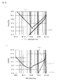
- the horizontal axis of the graph indicates the frequency [Hz], and the vertical axis indicates each value [ ⁇ ] of the absolute value Mag Z and the equivalent series resistance ESR.
- the measured value of the absolute value Mag Z is indicated by a solid characteristics line 31a, and the calculated value is indicated by a broken characteristics line 31b.
- the measured value of the equivalent series resistance ESR is indicated by a solid characteristics line 32a, and the calculated value is indicated by a broken characteristics line 32b.
- Fig. 5(b) is a graph illustrating the ratios between the aforementioned measured values and the calculated values indicated in Fig. 5(a) , in terms of the absolute value Mag Z and the equivalent series resistance ESR.
- the ratio in terms of the absolute value Mag Z is indicated by a solid characteristics line 31c, and the ratio in terms of the equivalent series resistance ESR is indicated by a broken characteristics line 32c.
- the ratios between the measured values and the calculated values are approximate to 1 over the entire band ranging from 100 [Hz] to 8.5 [GHz] in terms of both the absolute value Mag Z of the complex impedance Z and the equivalent series resistance ESR, and the calculated values fit well with the measured values.
- Fig. 6(a) is a graph illustrating a comparison between the calculated value obtained for the equivalent circuit model illustrated in Fig. 3 as a whole and a calculated value obtained for only the main resonant circuit 11A, in terms of the absolute value Mag Z of the complex impedance Z.
- Fig. 6(b) is a graph illustrating a comparison between the calculated value obtained for the equivalent circuit model illustrated in Fig. 3 as a whole and a calculated value obtained for only the main resonant circuit 11A, in terms of the equivalent series resistance ESR.
- each of the graphs indicates the frequency [Hz]
- the vertical axes indicate the value [ ⁇ ] of the absolute value Mag Z and the value [ ⁇ ] of the equivalent series resistance ESR.
- the calculated value obtained for the equivalent circuit model as a whole in terms of the absolute value Mag Z is indicated by the solid characteristics line 31b
- the calculated value in terms of the equivalent series resistance ESR is indicated by the solid characteristics line 32b.
- the calculated values indicated by the aforementioned characteristics lines 31b and 32b fit with the measured values.
- the calculated value obtained for only the main resonant circuit 11A in terms of the absolute value Mag Z is indicated by a broken characteristics line 31d
- the calculated value in terms of the equivalent series resistance ESR is indicated by a broken characteristics line 32d.
- Fig. 7(a) is a graph illustrating a comparison between the calculated value obtained for the equivalent circuit model illustrated in Fig. 3 as a whole and calculated values obtained for the parallel circuits 13A1 to 13A5 of the capacitive circuit 13A, in terms of the absolute value Mag Z of the complex impedance Z.
- Fig. 7(b) is a graph illustrating a comparison between the calculated value obtained for the equivalent circuit model illustrated in Fig. 3 as a whole and calculated values obtained for the parallel circuits 13A1 to 13A5 of the capacitive circuit 13A, in terms of the equivalent series resistance ESR.
- each of the graphs also indicates the frequency [Hz]
- the vertical axes indicate the value [ ⁇ ] of the absolute value Mag Z and the value [ ⁇ ] of the equivalent series resistance ESR.
- the calculated value obtained for the equivalent circuit model as a whole, which fits with the measured value, in terms of the absolute value Mag Z is also indicated by the solid characteristics line 31b
- the calculated value in terms of the equivalent series resistance ESR is indicated by the solid characteristics line 32b.
- the calculated values obtained for the parallel circuits 13A1, 13A2, 13A3, 13A4, and 13A5 of the capacitive circuit 13A in terms of the absolute value Mag Z are indicated, respectively, by broken characteristics lines 31e1, 31e2, 31e3, 31e4, and 31e5, and the calculated values in terms of the equivalent series resistance ESR are indicated by broken characteristics lines 32e1, 32e2, 32e3, 32e4, and 32e5.
- the ESR characteristics in a frequency band of a capacitive region at a lower frequency side of the self resonant frequency of the capacitor 1 fit with those of the characteristics line 32b obtained for the equivalent circuit model as a whole.
- the characteristics line 32d is largely offset from the characteristics line 32b in a frequency band at a lower frequency side capacitive region.
- Fig. 8(a) is a graph illustrating a comparison between the calculated value obtained for the equivalent circuit model illustrated in Fig. 3 as a whole and calculated values obtained for the parallel circuits 12A1 and 12A2 of the first secondary resonant circuit 12A, in terms of the absolute value Mag Z of the complex impedance Z.
- Fig. 8(b) is a graph illustrating a comparison between the calculated value obtained for the equivalent circuit model illustrated in Fig. 3 as a whole and calculated values obtained for the parallel circuits 12A1 and 12A2 of the first secondary resonant circuit 12A, in terms of the equivalent series resistance ESR.
- each of the graphs also indicates the frequency [Hz]
- the vertical axes indicate the value [ ⁇ ] of the absolute value Mag Z and the value [ ⁇ ] of the equivalent series resistance ESR.
- the calculated value obtained for the equivalent circuit model as a whole, which fits with the measured value, in terms of the absolute value Mag Z is indicated by the solid characteristics line 31b
- the calculated value in terms of the equivalent series resistance ESR is indicated by the solid characteristics line 32b.
- the calculated values obtained for the parallel circuits 12A1 and 12A2 of the first secondary resonant circuit 12A in terms of the absolute value Mag Z are indicated, respectively, by broken characteristics lines 31f1 and 31f2, and the calculated values in terms of the equivalent series resistance ESR are indicated by broken characteristics lines 32f1 and 32f2.
- the change in the characteristics protruding toward the upper side of the graph with a gentle curvature at a frequency around the secondary resonant frequency exceeding the self resonant frequency of the capacitor 1 fit with that of the measured value.
- the characteristics line 31d and the characteristics line 32d are unable to have such a change in the characteristics that protrudes toward the upper side of the graph with a gentle curvature, as in the characteristics lines 31b and 32b, at a frequency around the secondary resonant frequency exceeding the self resonant frequency.
- the characteristics indicated by the characteristics lines 31f1 and 31f2 illustrated in Fig. 8(a) and the characteristics indicated by the characteristics lines 32f1 and 32f2 illustrated in Fig. 8(b) are added to the characteristics indicated by the characteristics line 31d illustrated in Fig. 6(a) and by the characteristics line 32d illustrated in Fig. 6(b) , and thus the characteristics that protrude toward the upper side of the graph with a gentle curvature around the secondary resonant frequency exceeding the self resonant frequency can fit with those of the measured values.
- Fig. 9(a) is a graph illustrating a comparison between the calculated value obtained for the equivalent circuit model illustrated in Fig. 3 as a whole and calculated values obtained for the parallel circuits 14A1 to 14A3 of the inductive circuit 14A, in terms of the absolute value Mag Z of the complex impedance Z.
- Fig. 9(b) is a graph illustrating a comparison between the calculated value obtained for the equivalent circuit model illustrated in Fig. 3 as a whole and calculated values obtained for the parallel circuits 14A1 to 14A3 of the inductive circuit 14A, in terms of the equivalent series resistance ESR.
- each of the graphs also indicates the frequency [Hz]
- the vertical axes indicate the value [ ⁇ ] of the absolute value Mag Z and the value [ ⁇ ] of the equivalent series resistance ESR.
- the calculated value obtained for the equivalent circuit model as a whole, which fits with the measured value, in terms of the absolute value Mag Z is indicated by the solid characteristics line 31b
- the calculated value in terms of the equivalent series resistance ESR is indicated by the solid characteristics line 32b.
- the calculated values obtained for the parallel circuits 14A1, 14A2, and 14A3 of the inductive circuit 14A in terms of the absolute value Mag Z are indicated, respectively, by broken characteristics lines 31g1, 31g2, and 31g3, and the calculated values in terms of the equivalent series resistance ESR are indicated by broken characteristics lines 32g1, 32g2, and 32g3.
- the absolute value Mag Z characteristics and the ESR characteristics in a frequency band of an inductive region at a higher frequency side of the self resonant frequency of the capacitor 1 fit with those of the characteristics line 31b and the characteristics line 32b obtained for the equivalent circuit model as a whole.
- the characteristics line 31d and the characteristics line 32d are largely offset from the characteristics line 31b and the characteristics line 32b in a frequency band at a higher frequency side inductive region.
- Fig. 10(a) is a graph illustrating a comparison between the calculated value obtained for the equivalent circuit model illustrated in Fig. 3 as a whole and calculated values obtained for the parallel circuits 12B1 and 12B2 of the second secondary resonant circuit 12B, in terms of the absolute value Mag Z of the complex impedance Z.
- Fig. 10(b) is a graph illustrating a comparison between the calculated value obtained for the equivalent circuit model illustrated in Fig. 3 as a whole and calculated values obtained for the parallel circuits 12B1 and 12B2 of the second secondary resonant circuit 12B, in terms of the equivalent series resistance ESR.
- each of the graphs also indicates the frequency [Hz]
- the vertical axes indicate the value [ ⁇ ] of the absolute value Mag Z and the value [ ⁇ ] of the equivalent series resistance ESR.
- the calculated value obtained for the equivalent circuit model as a whole, which fits with the measured value, in terms of the absolute value Mag Z is indicated by the solid characteristics line 31b
- the calculated value in terms of the equivalent series resistance ESR is indicated by the solid characteristics line 32b.
- the calculated values obtained for the parallel circuits 12B1 and 12B2 of the second secondary resonant circuit 12B in terms of the absolute value Mag Z are indicated by broken characteristics lines 31h1 and 31h2, and the calculated values in terms of the equivalent series resistance ESR are indicated by broken characteristics lines 32h1 and 32h2.
- the absolute value Mag Z characteristics and the ESR characteristics in a frequency band at a higher frequency side of the self resonant frequency of the capacitor 1 fit with those of the measured values.
- the characteristics line 32h1 obtained for the parallel circuit 12B1 of the second secondary resonant circuit 12B contributes to the fitting of the ESR characteristics in a higher frequency band
- the characteristics line 31h2 obtained for the parallel circuit 12B2 contributes to the fine tuning of the absolute value Mag Z characteristics in a higher frequency side frequency band.
- the main resonant circuit 11A, the capacitive circuit 13A, the first secondary resonant circuit 12A, the inductive circuit 14A, and the second secondary resonant circuit 12B each exhibit the characteristics described above, and thus, as the equivalent circuit as a whole, the calculated values of the equivalent series resistance ESR and the absolute value Mag Z of the complex impedance Z held while the DC bias voltage v2 is not applied and fit well with the actual measured values, as illustrated in Fig. 5(a) .
- the DC bias voltage v2 ranging from 0 [V] to a rated voltage of 6.3 [V] was applied across the electrode terminals 3a and 3b of the capacitor 1, and the change in the characteristics of the capacitor 1 arising when each of the DC bias voltages v2 was applied was measured.
- the measurement was carried out by connecting a network analyzer between port-1 and port-2 and by applying the DC bias voltage v2 for 60 seconds at a measurement frequency of 1 [kHz] under a measurement temperature of 25 ⁇ 3°C.
- Table 1 below indicates the equivalent series capacitance C [ ⁇ F] and the dielectric loss tan ⁇ [%] of the capacitor 1 obtained through the calculation above, and the rate of change in the capacitance Kc [-] and the rate of change in the dielectric loss Kd [-] in terms of the characteristic values held while the DC bias voltage v2 is not applied.
- the rate of change in the capacitance Kc and the rate of change in the dielectric loss Kd are dimensionless quantities that do not have a dimension, and [-] indicates that these are dimensionless.
- Fig. 11(a) is a graph illustrating a comparison between a measured value and a calculated value obtained by using the equivalent circuit model illustrated in Fig. 3 , in terms of the absolute value Mag Z of the complex impedance Z of the capacitor 1 held when the DC bias voltage v2 is applied at the rated voltage of 6.3 [V].
- the horizontal axis of the graph indicates the frequency [Hz], and the vertical axis indicates the value [ ⁇ ] of the absolute value Mag Z.
- the measured value of the absolute value Mag Z obtained when the DC bias voltage v2 is 0 [V] is indicated by the solid characteristics line 31a
- the measured value of the absolute value Mag Z obtained when the DC bias voltage v2 is 6.3 [V] is indicated by a solid characteristics line 31i.
- the calculated value of the absolute value Mag Z obtained when the DC bias voltage v2 is 6.3 [V] is indicated by a broken characteristics line 31j.
- Fig. 11(b) is a graph illustrating a comparison between a measured value and a calculated value obtained by using the equivalent circuit model illustrated in Fig. 3 , in terms of the equivalent series resistance ESR of the capacitor 1 held when the DC bias voltage v2 is applied at the rated voltage of 6.3 [V].
- the horizontal axis of the graph indicates the frequency [Hz], and the vertical axis indicates the value [ ⁇ ] of the equivalent series resistance ESR.
- the measured value of the equivalent series resistance ESR obtained when the DC bias voltage v2 is 0 [V] is indicated by the solid characteristics line 32a
- the measured value of the equivalent series resistance ESR obtained when the DC bias voltage v2 is 6.3 [V] is indicated by a solid characteristics line 32i.
- the calculated value of the equivalent series resistance ESR obtained when the DC bias voltage v2 is 6.3 [V] is indicated by a broken characteristics line 32j.
- the calculated values indicated in the graphs have been obtained with the use of the deriving method according to the present embodiment, or by applying the dimensionless coefficient 15 obtained from the rate of change in the capacitance Kc and the rate of change in the dielectric loss Kd indicated in Table 1 in accordance with the application rule 16 described with reference to Figs. 2 and 3 .
- the calculated values, indicated by the characteristics lines 31j and 32j, of the absolute value Mag Z of the complex impedance Z and the equivalent series resistance ESR obtained when the DC bias voltage v2 is 6.3 [V] both fit well with the measured values indicated by the characteristics lines 31i and 32i obtained when the DC bias voltage v2 is 6.3 [V] over the entire band ranging from 100 [Hz] to 8.5 [GHz].
- Fig. 12(a) is a graph illustrating a ratio between a measured value obtained by using the measurement circuit illustrated in Fig. 4 and a calculated value obtained without employing the dimensionless coefficient 15 in accordance with the application rule 16, in terms of the absolute value Mag Z of the complex impedance Z of the capacitor 1 held when the DC bias voltage v2 is applied at three levels of 0 [V], 3.15 [V], and 6.3 [V].
- Fig. 12(b) is a graph illustrating a ratio between the measured value obtained by using the measurement circuit illustrated in Fig.
- the ratio obtained when the DC bias voltage v2 is 0 [V] is indicated by a solid characteristics line 31k; the ratio obtained when the DC bias voltage v2 is 3.15 [V] is indicated by a dashed characteristics line 31m; and the ratio obtained when the DC bias voltage v2 is 6.3 [V] is indicated by a dotted characteristics line 31n.
- the characteristics lines 31m and 31n obtained when the DC bias voltage v2 is applied are not approximate to 1 in a lower frequency side.
- the characteristics lines 31m and 31n obtained when the DC bias voltage v2 is applied could be made approximate to 1 throughout the entire frequency band.
- Fig. 13(a) is a graph illustrating a ratio between a measured value obtained by using the measurement circuit illustrated in Fig. 4 and a calculated value obtained without employing the dimensionless coefficient 15 in accordance with the application rule 16, in terms of the equivalent series resistance ESR of the capacitor 1 held when the DC bias voltage v2 is applied at three levels of 0 [V], 3.15 [V], and 6.3 [V].
- Fig. 13(b) is a graph illustrating a ratio between the measured value obtained by using the measurement circuit illustrated in Fig.
- the ratio obtained when the DC bias voltage v2 is 0 [V] is indicated by a solid characteristics line 32k; the ratio obtained when the DC bias voltage v2 is 3.15 [V] is indicated by a dashed characteristics line 32m; and the ratio obtained when the DC bias voltage v2 is 6.3 [V] is indicated by a dotted characteristics line 32n.
- the characteristics lines 32m and 32n obtained when the DC bias voltage v2 is applied are not approximate to 1 in a lower frequency side.
- the characteristics lines 32m and 32n obtained when the DC bias voltage v2 is applied could be made approximate to 1 throughout the entire frequency band.
- Fig. 14(a) is a graph illustrating the rate of change in the capacitance Kc of the capacitor 1 indicated in Table 1 being expressed as an approximate function of the DC bias voltage v2 applied to the capacitor 1.
- Fig. 14(b) is a graph illustrating the rate of change in the dielectric loss Kd of the capacitor 1 indicated in Table 1 being expressed as an approximate function of the DC bias voltage v2 applied to the capacitor 1.
- the horizontal axis in each of the graphs indicates the DC bias voltage v2 [V]
- the vertical axes indicate the rate of change in the capacitance Kc [%] and the rate of change in the dielectric loss Kd [%].
- the approximate function of the rate of change in the capacitance Kc is indicated by a characteristics line 41
- the approximate function of the rate of change in the dielectric loss Kd is indicated by a characteristics line 42.
- square plots indicate the measured values of the rate of change in the capacitance Kc and the rate of change in the dielectric loss Kd indicated in Table 1.
- the rate of change in the capacitance Kc and the rate of change in the dielectric loss Kd are expressed as the approximate functions above, the rate of change in the capacitance Kc and the rate of change in the dielectric loss Kd for any consecutive DC bias voltages v2 between the measured values obtained discretely as indicated in Table 1 can be complemented, and the dimensionless coefficient 15 for any consecutive DC bias voltages v2 can thus be obtained. Therefore, by multiplying the characteristic values of the resistive element R and the capacitive element C by the dimensionless coefficient 15 obtained as described above in accordance with the application rule 16 as described above, an equivalent circuit model for any consecutive DC bias voltages v2 can be derived, and the circuit characteristics can be calculated by using the derived equivalent circuit model.
- the aforementioned approximate function is set to a function representing a general form as in the following expression (3) in the present embodiment.
- variable x in the above expression (3) represents the DC bias voltage v2, and the function f(x) is expressed through the following expression (4).
- f x b 1 ⁇ g 1 x + ⁇ + b N ⁇ g N x
- a power of x (x n ) is often set as the basis function, a different basis function may be selected in a case in which the speed of conversion or the behavior of the function is to be restricted.
- the waveform may heave when the number of pieces of data is small, and thus the function indicated in the expression (5) is set as the basis function here, in place of a power of x (x n ).
- n is a natural number that is equal to or greater than 2 (n ⁇ 2).
- c and ⁇ x are constants, in which c > 0 and ⁇ x > 0, and are undetermined coefficients that are to be adjusted in accordance with the slope (steepness) of the function. It is to be noted that the basis function indicated here is a setting example and, in reality, is not limited to such an example.
- the horizontal axis of the graph indicates the variable x representing the DC bias voltage v2, and the vertical axis indicates the value of the basis function g n (x).
- g 1 (x) is linear
- g 2 (x), g 3 (x), g 4 (x), and g 5 (x) are curved so as to gradually approach a predetermined value.
- the rate of change in the capacitance Kc and the rate of change in the dielectric loss Kd gradually approach the predetermined value as the DC bias voltage v2 rises, as indicated by the graph illustrated in Fig. 14 , and can thus be approximated through the basis function g n (x) above.
- the characteristic values of the resistive elements R2 to R6 and the capacitive elements C1, C7, and C8 forming the equivalent circuit model of the capacitor 1 change in response to the DC bias voltage v2 being applied to the capacitor 1, and such a change is attributable to the material of the dielectric 2 forming the capacitor 1.
- the characteristic values of the resistive elements R2 to R6 and the capacitive elements C1, C7, and C8, of which the characteristic values change in response to the DC bias voltage v2 being applied held while the DC bias voltage v2 is not applied by the dimensionless coefficient 15 in accordance with the application rule 16 as described above, the characteristic values of the resistive elements R2 to R6 and the capacitive elements C1, C7, and C8 are corrected to values in accordance with the voltage of the DC bias voltage v2 applied to the capacitor 1.
- an equivalent circuit model does not need to be derived for each value of the DC bias voltage v2 superimposed and applied to the capacitor 1, and an equivalent circuit model having characteristics in accordance with the DC bias voltage v2 superimposed and applied to the capacitor 1 can be derived with high accuracy and with ease.
- the equivalent circuit model is formed by the main resonant circuit 11 and the secondary resonant circuit 12 serving as circuit elements, and the main resonant circuit 11 and the secondary resonant circuit 12 are each formed by a resistive element R, a capacitive element C, and an inductive element L.
- the characteristics of the capacitor 1 change as illustrated in Fig. 5(a) around the self resonant frequency or the secondary resonant frequency exceeding the self resonant frequency.
- the equivalent circuit model includes the main resonant circuit 11 and the secondary resonant circuit 12 serving as circuit elements, and the main resonant circuit 11 and the secondary resonant circuit 12 are each formed by a resistive element R, a capacitive element C, and an inductive element L.
- the change in the characteristics can be simulated accurately.
- the equivalent circuit model is formed by the main resonant circuit 11, the secondary resonant circuit 12, the capacitive circuit 13, and the inductive circuit 14 that are connected in series.
- the main resonant circuit 11 is formed by connecting a resistive element R, a capacitive element C, and an inductive element L in series;
- the secondary resonant circuit 12 is formed by connecting a resistive element R, a capacitive element C, and an inductive element L in parallel;
- the capacitive circuit 13 is formed by connecting a resistive element R and a capacitive element C in parallel;
- the inductive circuit 14 is formed by connecting a resistive element R and an inductive element L in parallel.
- the equivalent circuit model is formed so as to include the main resonant circuit 11, in accordance with the material of the dielectric 2 of the capacitor 1, the characteristics of the capacitor 1 at a frequency around the self resonant frequency are corrected appropriately, as illustrated in Fig. 6 .
- the equivalent circuit model is formed so as to include the capacitive circuit 13, in accordance with the material of the dielectric 2 of the capacitor 1, the characteristics at a frequency toward a lower frequency side of the self resonant frequency are corrected appropriately, as illustrated in Fig. 7 .
- the equivalent circuit model is formed so as to include the secondary resonant circuit 12, in accordance with the material of the dielectric 2 of the capacitor 1, the characteristics at a frequency around the secondary resonant frequency exceeding the self resonant frequency are corrected appropriately, as illustrated in Fig. 8 .
- the equivalent circuit model is formed so as to include the inductive circuit 14, in accordance with the material of the dielectric 2 of the capacitor 1, the characteristics at a frequency toward a higher frequency side of the self resonant frequency are corrected appropriately, as illustrated in Fig. 9 .
- the dimensionless coefficient 15 is expressed for the resistive elements R2 to R6 and the capacitive elements C1, C7, and C8, of which the characteristic values change in response to the DC bias voltage v2 being applied to the capacitor 1, on the basis of one or both of the rate of change in the capacitance Kc and the rate of change in the dielectric loss Kd of the capacitor 1, which are measured by applying the DC bias voltage v2 to the capacitor 1.
- the characteristic values of these elements are then corrected by multiplying the capacitance values of the capacitive elements C1, C7, and C8, of which the capacitance values change in accordance with the DC bias voltage v2, held while the DC bias voltage v2 is not applied and the resistance values of the resistive elements R2 to R6, of which the resistance values change in accordance with the DC bias voltage v2, held while the DC bias voltage v2 is not applied by the dimensionless coefficient 15.
- the capacitance values and the resistance values of the capacitive elements C1, C7, and C8 and the resistive elements R2 to R6, of which the characteristic values change in response to the DC bias voltage v2 being applied to the capacitor 1, are corrected appropriately to values in accordance with the DC bias voltage v2 to be superimposed and applied to the capacitor 1 as the characteristic values held while the DC bias voltage v2 is not applied to the capacitor 1 is multiplied by the dimensionless coefficient 15.
- the rate of change in the capacitance Kc which is a rate of change in the characteristic values of the capacitive elements C1, C7, and C8, and the rate of change in the dielectric loss Kd, which is a rate of change in the characteristic values of the resistive elements R2 to R6, are expressed, for example, through the expressions (7) and (8) as the approximate functions of the DC bias voltage v2 applied to the capacitor 1.
- the approximate function of which the general form is indicated in the expressions (3) and (4), is expressed in a direct current voltage range that ranges from the rated voltage of the capacitor 1 or lower to zero or higher, and the function value always takes a positive value and becomes 1 when the DC bias voltage v2 applied to the capacitor 1 is zero.
- the dielectric 2 of the capacitor 1 is formed of ceramics.
- the material of the dielectric 2 of the capacitor 1, however, is not limited to ceramics, and the present invention can be applied, in a similar manner, to a capacitor that is formed by a dielectric made of a different material.
- the equivalent circuit model is formed as an impedance expansion type equivalent circuit model by connecting the main resonant circuit 11, the secondary resonant circuit 12, the capacitive circuit 13, and the inductive circuit 14 in series, as illustrated in Fig. 2 .
- the equivalent circuit model may be formed by one of the aforementioned circuits in accordance with the material of the dielectric 2 of the capacitor 1.
- the equivalent circuit model may be formed by connecting some of the aforementioned circuits in series.
- a resistive element R14 and a capacitive element C11 serving as floating components, may additionally be connected in parallel to the series circuit formed by the main resonant circuit 11, the secondary resonant circuit 12, the capacitive circuit 13, and the inductive circuit 14.
- a resistive element R15 serving as an insulation resistance, may additionally be connected in parallel to the capacitive element C of the main resonant circuit 11.
- the equivalent circuit model of an admittance expansion type may be formed by connecting a main resonant circuit 51, an secondary resonant circuit 52, a capacitive circuit 53, and an inductive circuit 54 in parallel between the electrode terminals 3a and 3b.
- the main resonant circuit 51 is formed by connecting a resistive element R, a capacitive element C, and an inductive element L in parallel;
- the secondary resonant circuit 52 is formed by connecting a resistive element R, a capacitive element C, and an inductive element L in series;
- the capacitive circuit 53 is formed by connecting a resistive element R and a capacitive element C in series;
- the inductive circuit 54 is formed by connecting a resistive element R and an inductive element L in series.
- the equivalent circuit model may be formed by one of the aforementioned circuits in accordance with the material of the dielectric 2 of the capacitor 1.
- the equivalent circuit model may be formed by connecting some of the aforementioned circuits in series.
- the equivalent circuit model is formed so as to include the main resonant circuit 51, in accordance with the material of the dielectric 2 of the capacitor 1, the characteristics at a frequency around the self resonant frequency are corrected appropriately. Additionally, as the equivalent circuit model is formed so as to include the capacitive circuit 53, in accordance with the material of the dielectric 2 of the capacitor 1, the characteristics at a frequency toward a lower frequency side of the self resonant frequency are corrected appropriately.
- the equivalent circuit model is formed so as to include the secondary resonant circuit 52, in accordance with the material of the dielectric 2 of the capacitor 1, the characteristics at a frequency around the secondary resonant frequency exceeding the self resonant frequency are corrected appropriately.
- the equivalent circuit model is formed so as to include the inductive circuit 54, in accordance with the material of the dielectric 2 of the capacitor 1, the characteristics at a frequency toward a higher frequency side of the self resonant frequency are corrected appropriately.
- the characteristic value of the resistive element R, the capacitive element C, or the inductive element L, of which the characteristic value changes in response to the DC bias voltage v2 being applied to the capacitor 1 held while the DC bias voltage v2 is not applied by a dimensionless coefficient in accordance with a predetermined application rule, the characteristic value of the resistive element R, the capacitive element C, or the inductive element L, of which the characteristic value changes in accordance with the DC bias voltage v2, is corrected to a value in accordance with the voltage of the DC bias voltage v2 applied to the capacitor 1.
- the equivalent circuit model may be formed by additionally connecting a resistive element R16 and an inductive element L9, serving as floating components, in series to each of the circuits.
- a resistive element R17 serving as an insulation resistance, may additionally be connected in series to the inductive element L of the main resonant circuit 51.
- the method for deriving an equivalent circuit model according to the present embodiment described above can be implemented with ease by using the following computer program.
- the computer program includes a first step of inputting the type of the capacitor 1 to be used for designing an electronic circuit, a second step of inputting the value of the DC bias voltage v2 to be applied to the capacitor 1, and a third step of multiplying the characteristic value of a circuit element forming the equivalent circuit model of the capacitor 1 of the type inputted in the first step held while the DC bias voltage v2 is not applied by the dimensionless coefficient 15 that is prepared in advance in a memory for the capacitor 1 of the type inputted in the first step, as in the present embodiment described above, and correcting the characteristic value of the circuit element to a value in accordance with the DC bias voltage v2 inputted in the second step, and thus the method for deriving the equivalent circuit model according to the present embodiment described above is made function.
- the method for deriving the equivalent circuit model of the capacitor according to the present embodiment is made function by the computer program simply as the type of the capacitor 1 to be simulated and the value of the DC bias voltage v2 to be applied to the capacitor 1 are inputted to the computer program, as described above. Therefore, the characteristic value of the circuit element forming the equivalent circuit model of the capacitor 1 of the inputted type is automatically corrected to a value in accordance with the inputted value of the DC bias voltage v2 by the computer program as the characteristic value held while the DC bias voltage v2 is not applied is multiplied by the dimensionless coefficient 15 prepared in advance for the capacitor 1 of the inputted type.
- a user of the deriving method can carry out an appropriate circuit simulation with high accuracy and with ease only by inputting the type of the capacitor 1 to be simulated and the value of the DC bias voltage v2 to be applied to the capacitor 1 to the computer program.
- a general user who does not have specialized knowledge on a circuit simulation can carry out an appropriate circuit simulation for an electronic circuit that includes the capacitor 1 with high accuracy and with ease.
- the computer program described above can be used from a terminal, such as a personal computer, connected to the Internet by accessing a server of an electronic component manufacturer or the like provided with the computer program through the Internet.
- a terminal such as a personal computer
- the user can use the computer program with ease by accessing the server provided with the computer program from a terminal connected to the Internet. Accordingly, the method for deriving the equivalent circuit model of the capacitor according to the present embodiment can be provided to a large number of users.
Landscapes
- Engineering & Computer Science (AREA)
- Computer Hardware Design (AREA)
- Physics & Mathematics (AREA)
- Theoretical Computer Science (AREA)
- Evolutionary Computation (AREA)
- Geometry (AREA)
- General Engineering & Computer Science (AREA)
- General Physics & Mathematics (AREA)
- Microelectronics & Electronic Packaging (AREA)
- Power Engineering (AREA)
- Chemical & Material Sciences (AREA)
- Manufacturing & Machinery (AREA)
- Ceramic Engineering (AREA)
- Inorganic Chemistry (AREA)
- Fixed Capacitors And Capacitor Manufacturing Machines (AREA)
- Measurement Of Resistance Or Impedance (AREA)
- Filters And Equalizers (AREA)
Applications Claiming Priority (2)
| Application Number | Priority Date | Filing Date | Title |
|---|---|---|---|
| JP2012085478 | 2012-04-04 | ||
| PCT/JP2013/054823 WO2013150833A1 (fr) | 2012-04-04 | 2013-02-25 | Procédé d'obtention d'un modèle de circuit équivalent d'un condensateur |
Publications (3)
| Publication Number | Publication Date |
|---|---|
| EP2835749A1 true EP2835749A1 (fr) | 2015-02-11 |
| EP2835749A4 EP2835749A4 (fr) | 2016-01-06 |
| EP2835749B1 EP2835749B1 (fr) | 2019-04-10 |
Family
ID=49300333
Family Applications (1)
| Application Number | Title | Priority Date | Filing Date |
|---|---|---|---|
| EP13772567.7A Active EP2835749B1 (fr) | 2012-04-04 | 2013-02-25 | Procédé d'obtention d'un modèle de circuit équivalent d'un condensateur |
Country Status (6)
| Country | Link |
|---|---|
| US (1) | US9355210B2 (fr) |
| EP (1) | EP2835749B1 (fr) |
| JP (1) | JP5861774B2 (fr) |
| KR (1) | KR101643898B1 (fr) |
| CN (1) | CN104246777B (fr) |
| WO (1) | WO2013150833A1 (fr) |
Families Citing this family (9)
| Publication number | Priority date | Publication date | Assignee | Title |
|---|---|---|---|---|
| KR101616037B1 (ko) * | 2013-05-14 | 2016-04-27 | 가부시키가이샤 무라타 세이사쿠쇼 | 콘덴서의 시뮬레이션 방법 및 콘덴서의 비선형 등가 회로 모델 |
| CN105181219B (zh) * | 2015-08-11 | 2018-01-30 | 中国电子科技集团公司第四十一研究所 | 一种可工作于超高温环境下的压力参数提取装置 |
| DE102016110742A1 (de) * | 2016-06-10 | 2017-12-14 | Epcos Ag | Filterbauelement zur Filterung eines Störsignals |
| JP6238257B1 (ja) * | 2016-06-28 | 2017-11-29 | 三菱電機株式会社 | 電力変換装置 |
| JP6797656B2 (ja) * | 2016-12-09 | 2020-12-09 | 矢崎総業株式会社 | 差電圧測定装置 |
| CN107478911B (zh) * | 2017-09-05 | 2020-08-11 | 国网河南省电力公司检修公司 | 一种基于谐波测量高压电容器容值的方法和系统 |
| JP7276284B2 (ja) * | 2020-08-27 | 2023-05-18 | 株式会社村田製作所 | 積層コンデンサのシミュレーションモデルの生成方法、および、積層コンデンサのシミュレーション方法 |
| CN114492270A (zh) * | 2020-10-26 | 2022-05-13 | 丰宾电子(深圳)有限公司 | 一种电容用于5g电路应用等效模型的建模电路及方法 |
| CN115169281B (zh) * | 2022-07-19 | 2025-06-17 | 南京师范大学 | 基于soma的主振动模式下压电材料等效电路建模方法 |
Family Cites Families (8)
| Publication number | Priority date | Publication date | Assignee | Title |
|---|---|---|---|---|
| JP4507421B2 (ja) | 2001-02-27 | 2010-07-21 | パナソニック株式会社 | 受動素子の等価回路モデル導出方法、シミュレータ、及び記憶媒体 |
| JP2003022295A (ja) * | 2001-07-06 | 2003-01-24 | Mitsubishi Electric Corp | 実効値インピーダンス模擬方法および装置並びに実効値インピーダンス模擬用プログラム |
| US7474999B2 (en) * | 2002-12-23 | 2009-01-06 | Cadence Design Systems, Inc. | Method for accounting for process variation in the design of integrated circuits |
| CN100401306C (zh) * | 2005-12-05 | 2008-07-09 | 华为技术有限公司 | 一种电容等效模型的建模装置和方法 |
| JP5475563B2 (ja) * | 2010-06-15 | 2014-04-16 | 太陽誘電株式会社 | 積層チップコンデンサの回路定数解析プログラム及び回路定数解析装置 |
| WO2012024517A1 (fr) * | 2010-08-18 | 2012-02-23 | Wispry, Inc. | Procédés de réglage pour réseaux d'adaptation réglables |
| CN103282904B (zh) | 2010-12-29 | 2016-01-20 | 株式会社村田制作所 | 等效电路模型,程序以及存储介质 |
| JP2012150579A (ja) * | 2011-01-17 | 2012-08-09 | Taiyo Yuden Co Ltd | コンデンサの回路シミュレーションモデル及びその構築方法,回路シミュレーション方法及び回路シミュレータ |
-
2013
- 2013-02-25 JP JP2014509077A patent/JP5861774B2/ja active Active
- 2013-02-25 EP EP13772567.7A patent/EP2835749B1/fr active Active
- 2013-02-25 WO PCT/JP2013/054823 patent/WO2013150833A1/fr not_active Ceased
- 2013-02-25 CN CN201380018415.5A patent/CN104246777B/zh active Active
- 2013-02-25 KR KR1020147027601A patent/KR101643898B1/ko active Active
-
2014
- 2014-09-19 US US14/491,756 patent/US9355210B2/en active Active
Also Published As
| Publication number | Publication date |
|---|---|
| CN104246777B (zh) | 2017-06-27 |
| KR101643898B1 (ko) | 2016-07-29 |
| US9355210B2 (en) | 2016-05-31 |
| EP2835749A4 (fr) | 2016-01-06 |
| KR20140131568A (ko) | 2014-11-13 |
| CN104246777A (zh) | 2014-12-24 |
| JPWO2013150833A1 (ja) | 2015-12-17 |
| EP2835749B1 (fr) | 2019-04-10 |
| WO2013150833A1 (fr) | 2013-10-10 |
| US20150012899A1 (en) | 2015-01-08 |
| JP5861774B2 (ja) | 2016-02-16 |
Similar Documents
| Publication | Publication Date | Title |
|---|---|---|
| EP2835749A1 (fr) | Procédé d'obtention d'un modèle de circuit équivalent d'un condensateur | |
| US10521533B2 (en) | Inductor simulation method and inductor nonlinear equivalent circuit model | |
| US8718987B2 (en) | Circuit simulation model of capacitor, constructing method of simulation model, method of circuit simulation, circuit simulator | |
| US20160063159A1 (en) | Capacitor simulation method and capacitor nonlinear equivalent circuit model | |
| US9563728B2 (en) | Equivalent circuit model, program, and recording medium | |
| JP2004235279A (ja) | インダクタ素子のシミュレーション方法及びその等価回路 | |
| Lakshminarayanan et al. | A substrate-dependent CAD model for ceramic multilayer capacitors | |
| Prymak | SPICE modeling of capacitors | |
| Prymak et al. | Capacitor EDA models with compensations for frequency, temperature, and DC bias | |
| US7107555B2 (en) | Method and apparatus for designing high-frequency circuit, and display method for use in designing high-frequency circuit | |
| CN105453088B (zh) | 考虑到施加交流电压的电容器的静电电容值决定方法及程序 | |
| Kim et al. | Characterization of discrete decoupling capacitors for high-speed digital systems | |
| JP2017091346A (ja) | インダクタのシミュレーションモデル | |
| Raghavendra et al. | Characterization of novel varistor+ inductor integrated passive devices | |
| Walczak et al. | Analysis of parallel resonance RLC α circuit with supercapacitor | |
| Ng et al. | A wide frequency band characterization technique for multiple-terminal discrete decoupling capacitors | |
| Bishnoi et al. | EMI modeling of buck converter using a generalized terminal model | |
| Raouf | Completely automated system for capacitance measurement through new accurate capacitance box | |
| Hayes et al. | TECHNICAL REPORT: CVEL-17-069 | |
| JP2025043940A (ja) | 等価回路 | |
| Winiarski et al. | AC properties of low-pass RC filters embedded in printed circuit boards | |
| Lapuh et al. | Analysis and improvements of precision coaxial current shunts for direct measurement of ac current | |
| Capacitors | DesignCon 2006 | |
| Olver et al. | Simplify Selection and Improve Reliability of Small Form Factor Resistors, Capacitors, and Magnetics Used in Medical Devices | |
| KR20050094173A (ko) | 비선형 특성을 표현하는 콘덴서의 등가회로 |
Legal Events
| Date | Code | Title | Description |
|---|---|---|---|
| PUAI | Public reference made under article 153(3) epc to a published international application that has entered the european phase |
Free format text: ORIGINAL CODE: 0009012 |
|
| 17P | Request for examination filed |
Effective date: 20140821 |
|
| AK | Designated contracting states |
Kind code of ref document: A1 Designated state(s): AL AT BE BG CH CY CZ DE DK EE ES FI FR GB GR HR HU IE IS IT LI LT LU LV MC MK MT NL NO PL PT RO RS SE SI SK SM TR |
|
| AX | Request for extension of the european patent |
Extension state: BA ME |
|
| DAX | Request for extension of the european patent (deleted) | ||
| RA4 | Supplementary search report drawn up and despatched (corrected) |
Effective date: 20151209 |
|
| RIC1 | Information provided on ipc code assigned before grant |
Ipc: H01G 4/12 20060101ALI20151203BHEP Ipc: G06F 17/50 20060101AFI20151203BHEP Ipc: H01G 4/30 20060101ALI20151203BHEP |
|
| 17Q | First examination report despatched |
Effective date: 20160825 |
|
| STAA | Information on the status of an ep patent application or granted ep patent |
Free format text: STATUS: EXAMINATION IS IN PROGRESS |
|
| GRAP | Despatch of communication of intention to grant a patent |
Free format text: ORIGINAL CODE: EPIDOSNIGR1 |
|
| STAA | Information on the status of an ep patent application or granted ep patent |
Free format text: STATUS: GRANT OF PATENT IS INTENDED |
|
| RIC1 | Information provided on ipc code assigned before grant |
Ipc: H01G 4/30 20060101ALI20180904BHEP Ipc: H01G 4/255 20060101ALI20180904BHEP Ipc: H01G 4/12 20060101ALI20180904BHEP Ipc: G06F 17/50 20060101AFI20180904BHEP |
|
| INTG | Intention to grant announced |
Effective date: 20180925 |
|
| GRAS | Grant fee paid |
Free format text: ORIGINAL CODE: EPIDOSNIGR3 |
|
| GRAA | (expected) grant |
Free format text: ORIGINAL CODE: 0009210 |
|
| STAA | Information on the status of an ep patent application or granted ep patent |
Free format text: STATUS: THE PATENT HAS BEEN GRANTED |
|
| AK | Designated contracting states |
Kind code of ref document: B1 Designated state(s): AL AT BE BG CH CY CZ DE DK EE ES FI FR GB GR HR HU IE IS IT LI LT LU LV MC MK MT NL NO PL PT RO RS SE SI SK SM TR |
|
| REG | Reference to a national code |
Ref country code: GB Ref legal event code: FG4D |
|
| REG | Reference to a national code |
Ref country code: CH Ref legal event code: EP Ref country code: AT Ref legal event code: REF Ref document number: 1119652 Country of ref document: AT Kind code of ref document: T Effective date: 20190415 |
|
| REG | Reference to a national code |
Ref country code: IE Ref legal event code: FG4D |
|
| REG | Reference to a national code |
Ref country code: DE Ref legal event code: R096 Ref document number: 602013053738 Country of ref document: DE |
|
| REG | Reference to a national code |
Ref country code: NL Ref legal event code: MP Effective date: 20190410 |
|
| REG | Reference to a national code |
Ref country code: LT Ref legal event code: MG4D |
|
| REG | Reference to a national code |
Ref country code: AT Ref legal event code: MK05 Ref document number: 1119652 Country of ref document: AT Kind code of ref document: T Effective date: 20190410 |
|
| PG25 | Lapsed in a contracting state [announced via postgrant information from national office to epo] |
Ref country code: NL Free format text: LAPSE BECAUSE OF FAILURE TO SUBMIT A TRANSLATION OF THE DESCRIPTION OR TO PAY THE FEE WITHIN THE PRESCRIBED TIME-LIMIT Effective date: 20190410 |
|
| PG25 | Lapsed in a contracting state [announced via postgrant information from national office to epo] |
Ref country code: FI Free format text: LAPSE BECAUSE OF FAILURE TO SUBMIT A TRANSLATION OF THE DESCRIPTION OR TO PAY THE FEE WITHIN THE PRESCRIBED TIME-LIMIT Effective date: 20190410 Ref country code: NO Free format text: LAPSE BECAUSE OF FAILURE TO SUBMIT A TRANSLATION OF THE DESCRIPTION OR TO PAY THE FEE WITHIN THE PRESCRIBED TIME-LIMIT Effective date: 20190710 Ref country code: PT Free format text: LAPSE BECAUSE OF FAILURE TO SUBMIT A TRANSLATION OF THE DESCRIPTION OR TO PAY THE FEE WITHIN THE PRESCRIBED TIME-LIMIT Effective date: 20190910 Ref country code: AL Free format text: LAPSE BECAUSE OF FAILURE TO SUBMIT A TRANSLATION OF THE DESCRIPTION OR TO PAY THE FEE WITHIN THE PRESCRIBED TIME-LIMIT Effective date: 20190410 Ref country code: SE Free format text: LAPSE BECAUSE OF FAILURE TO SUBMIT A TRANSLATION OF THE DESCRIPTION OR TO PAY THE FEE WITHIN THE PRESCRIBED TIME-LIMIT Effective date: 20190410 Ref country code: HR Free format text: LAPSE BECAUSE OF FAILURE TO SUBMIT A TRANSLATION OF THE DESCRIPTION OR TO PAY THE FEE WITHIN THE PRESCRIBED TIME-LIMIT Effective date: 20190410 Ref country code: LT Free format text: LAPSE BECAUSE OF FAILURE TO SUBMIT A TRANSLATION OF THE DESCRIPTION OR TO PAY THE FEE WITHIN THE PRESCRIBED TIME-LIMIT Effective date: 20190410 Ref country code: ES Free format text: LAPSE BECAUSE OF FAILURE TO SUBMIT A TRANSLATION OF THE DESCRIPTION OR TO PAY THE FEE WITHIN THE PRESCRIBED TIME-LIMIT Effective date: 20190410 |
|
| REG | Reference to a national code |
Ref country code: DE Ref legal event code: R079 Ref document number: 602013053738 Country of ref document: DE Free format text: PREVIOUS MAIN CLASS: G06F0017500000 Ipc: G06F0030000000 |
|
| PG25 | Lapsed in a contracting state [announced via postgrant information from national office to epo] |
Ref country code: PL Free format text: LAPSE BECAUSE OF FAILURE TO SUBMIT A TRANSLATION OF THE DESCRIPTION OR TO PAY THE FEE WITHIN THE PRESCRIBED TIME-LIMIT Effective date: 20190410 Ref country code: RS Free format text: LAPSE BECAUSE OF FAILURE TO SUBMIT A TRANSLATION OF THE DESCRIPTION OR TO PAY THE FEE WITHIN THE PRESCRIBED TIME-LIMIT Effective date: 20190410 Ref country code: BG Free format text: LAPSE BECAUSE OF FAILURE TO SUBMIT A TRANSLATION OF THE DESCRIPTION OR TO PAY THE FEE WITHIN THE PRESCRIBED TIME-LIMIT Effective date: 20190710 Ref country code: GR Free format text: LAPSE BECAUSE OF FAILURE TO SUBMIT A TRANSLATION OF THE DESCRIPTION OR TO PAY THE FEE WITHIN THE PRESCRIBED TIME-LIMIT Effective date: 20190711 Ref country code: LV Free format text: LAPSE BECAUSE OF FAILURE TO SUBMIT A TRANSLATION OF THE DESCRIPTION OR TO PAY THE FEE WITHIN THE PRESCRIBED TIME-LIMIT Effective date: 20190410 |
|
| PG25 | Lapsed in a contracting state [announced via postgrant information from national office to epo] |
Ref country code: AT Free format text: LAPSE BECAUSE OF FAILURE TO SUBMIT A TRANSLATION OF THE DESCRIPTION OR TO PAY THE FEE WITHIN THE PRESCRIBED TIME-LIMIT Effective date: 20190410 Ref country code: IS Free format text: LAPSE BECAUSE OF FAILURE TO SUBMIT A TRANSLATION OF THE DESCRIPTION OR TO PAY THE FEE WITHIN THE PRESCRIBED TIME-LIMIT Effective date: 20190810 |
|
| REG | Reference to a national code |
Ref country code: DE Ref legal event code: R097 Ref document number: 602013053738 Country of ref document: DE |
|
| PG25 | Lapsed in a contracting state [announced via postgrant information from national office to epo] |
Ref country code: RO Free format text: LAPSE BECAUSE OF FAILURE TO SUBMIT A TRANSLATION OF THE DESCRIPTION OR TO PAY THE FEE WITHIN THE PRESCRIBED TIME-LIMIT Effective date: 20190410 Ref country code: SK Free format text: LAPSE BECAUSE OF FAILURE TO SUBMIT A TRANSLATION OF THE DESCRIPTION OR TO PAY THE FEE WITHIN THE PRESCRIBED TIME-LIMIT Effective date: 20190410 Ref country code: CZ Free format text: LAPSE BECAUSE OF FAILURE TO SUBMIT A TRANSLATION OF THE DESCRIPTION OR TO PAY THE FEE WITHIN THE PRESCRIBED TIME-LIMIT Effective date: 20190410 Ref country code: EE Free format text: LAPSE BECAUSE OF FAILURE TO SUBMIT A TRANSLATION OF THE DESCRIPTION OR TO PAY THE FEE WITHIN THE PRESCRIBED TIME-LIMIT Effective date: 20190410 Ref country code: DK Free format text: LAPSE BECAUSE OF FAILURE TO SUBMIT A TRANSLATION OF THE DESCRIPTION OR TO PAY THE FEE WITHIN THE PRESCRIBED TIME-LIMIT Effective date: 20190410 |
|
| PLBE | No opposition filed within time limit |
Free format text: ORIGINAL CODE: 0009261 |
|
| STAA | Information on the status of an ep patent application or granted ep patent |
Free format text: STATUS: NO OPPOSITION FILED WITHIN TIME LIMIT |
|
| PG25 | Lapsed in a contracting state [announced via postgrant information from national office to epo] |
Ref country code: IT Free format text: LAPSE BECAUSE OF FAILURE TO SUBMIT A TRANSLATION OF THE DESCRIPTION OR TO PAY THE FEE WITHIN THE PRESCRIBED TIME-LIMIT Effective date: 20190410 Ref country code: SM Free format text: LAPSE BECAUSE OF FAILURE TO SUBMIT A TRANSLATION OF THE DESCRIPTION OR TO PAY THE FEE WITHIN THE PRESCRIBED TIME-LIMIT Effective date: 20190410 |
|
| 26N | No opposition filed |
Effective date: 20200113 |
|
| PG25 | Lapsed in a contracting state [announced via postgrant information from national office to epo] |
Ref country code: TR Free format text: LAPSE BECAUSE OF FAILURE TO SUBMIT A TRANSLATION OF THE DESCRIPTION OR TO PAY THE FEE WITHIN THE PRESCRIBED TIME-LIMIT Effective date: 20190410 |
|
| PG25 | Lapsed in a contracting state [announced via postgrant information from national office to epo] |
Ref country code: SI Free format text: LAPSE BECAUSE OF FAILURE TO SUBMIT A TRANSLATION OF THE DESCRIPTION OR TO PAY THE FEE WITHIN THE PRESCRIBED TIME-LIMIT Effective date: 20190410 |
|
| REG | Reference to a national code |
Ref country code: CH Ref legal event code: PL |
|
| GBPC | Gb: european patent ceased through non-payment of renewal fee |
Effective date: 20200225 |
|
| REG | Reference to a national code |
Ref country code: BE Ref legal event code: MM Effective date: 20200229 |
|
| PG25 | Lapsed in a contracting state [announced via postgrant information from national office to epo] |
Ref country code: LU Free format text: LAPSE BECAUSE OF NON-PAYMENT OF DUE FEES Effective date: 20200225 Ref country code: MC Free format text: LAPSE BECAUSE OF FAILURE TO SUBMIT A TRANSLATION OF THE DESCRIPTION OR TO PAY THE FEE WITHIN THE PRESCRIBED TIME-LIMIT Effective date: 20190410 |
|
| PG25 | Lapsed in a contracting state [announced via postgrant information from national office to epo] |
Ref country code: LI Free format text: LAPSE BECAUSE OF NON-PAYMENT OF DUE FEES Effective date: 20200229 Ref country code: CH Free format text: LAPSE BECAUSE OF NON-PAYMENT OF DUE FEES Effective date: 20200229 |
|
| PG25 | Lapsed in a contracting state [announced via postgrant information from national office to epo] |
Ref country code: FR Free format text: LAPSE BECAUSE OF NON-PAYMENT OF DUE FEES Effective date: 20200229 Ref country code: GB Free format text: LAPSE BECAUSE OF NON-PAYMENT OF DUE FEES Effective date: 20200225 Ref country code: IE Free format text: LAPSE BECAUSE OF NON-PAYMENT OF DUE FEES Effective date: 20200225 |
|
| PG25 | Lapsed in a contracting state [announced via postgrant information from national office to epo] |
Ref country code: BE Free format text: LAPSE BECAUSE OF NON-PAYMENT OF DUE FEES Effective date: 20200229 |
|
| PG25 | Lapsed in a contracting state [announced via postgrant information from national office to epo] |
Ref country code: MT Free format text: LAPSE BECAUSE OF FAILURE TO SUBMIT A TRANSLATION OF THE DESCRIPTION OR TO PAY THE FEE WITHIN THE PRESCRIBED TIME-LIMIT Effective date: 20190410 Ref country code: CY Free format text: LAPSE BECAUSE OF FAILURE TO SUBMIT A TRANSLATION OF THE DESCRIPTION OR TO PAY THE FEE WITHIN THE PRESCRIBED TIME-LIMIT Effective date: 20190410 |
|
| PG25 | Lapsed in a contracting state [announced via postgrant information from national office to epo] |
Ref country code: MK Free format text: LAPSE BECAUSE OF FAILURE TO SUBMIT A TRANSLATION OF THE DESCRIPTION OR TO PAY THE FEE WITHIN THE PRESCRIBED TIME-LIMIT Effective date: 20190410 |
|
| PGFP | Annual fee paid to national office [announced via postgrant information from national office to epo] |
Ref country code: DE Payment date: 20260218 Year of fee payment: 14 |