EP2835831A2 - Affichage à diodes électroluminescentes organiques - Google Patents
Affichage à diodes électroluminescentes organiques Download PDFInfo
- Publication number
- EP2835831A2 EP2835831A2 EP14180162.1A EP14180162A EP2835831A2 EP 2835831 A2 EP2835831 A2 EP 2835831A2 EP 14180162 A EP14180162 A EP 14180162A EP 2835831 A2 EP2835831 A2 EP 2835831A2
- Authority
- EP
- European Patent Office
- Prior art keywords
- common voltage
- voltage line
- light emitting
- electrode
- organic light
- Prior art date
- Legal status (The legal status is an assumption and is not a legal conclusion. Google has not performed a legal analysis and makes no representation as to the accuracy of the status listed.)
- Granted
Links
Images


Classifications
-
- H—ELECTRICITY
- H10—SEMICONDUCTOR DEVICES; ELECTRIC SOLID-STATE DEVICES NOT OTHERWISE PROVIDED FOR
- H10D—INORGANIC ELECTRIC SEMICONDUCTOR DEVICES
- H10D86/00—Integrated devices formed in or on insulating or conducting substrates, e.g. formed in silicon-on-insulator [SOI] substrates or on stainless steel or glass substrates
- H10D86/40—Integrated devices formed in or on insulating or conducting substrates, e.g. formed in silicon-on-insulator [SOI] substrates or on stainless steel or glass substrates characterised by multiple TFTs
- H10D86/451—Integrated devices formed in or on insulating or conducting substrates, e.g. formed in silicon-on-insulator [SOI] substrates or on stainless steel or glass substrates characterised by multiple TFTs characterised by the compositions or shapes of the interlayer dielectrics
-
- H—ELECTRICITY
- H10—SEMICONDUCTOR DEVICES; ELECTRIC SOLID-STATE DEVICES NOT OTHERWISE PROVIDED FOR
- H10K—ORGANIC ELECTRIC SOLID-STATE DEVICES
- H10K59/00—Integrated devices, or assemblies of multiple devices, comprising at least one organic light-emitting element covered by group H10K50/00
- H10K59/80—Constructional details
- H10K59/87—Passivation; Containers; Encapsulations
- H10K59/873—Encapsulations
-
- H—ELECTRICITY
- H10—SEMICONDUCTOR DEVICES; ELECTRIC SOLID-STATE DEVICES NOT OTHERWISE PROVIDED FOR
- H10D—INORGANIC ELECTRIC SEMICONDUCTOR DEVICES
- H10D86/00—Integrated devices formed in or on insulating or conducting substrates, e.g. formed in silicon-on-insulator [SOI] substrates or on stainless steel or glass substrates
- H10D86/40—Integrated devices formed in or on insulating or conducting substrates, e.g. formed in silicon-on-insulator [SOI] substrates or on stainless steel or glass substrates characterised by multiple TFTs
- H10D86/60—Integrated devices formed in or on insulating or conducting substrates, e.g. formed in silicon-on-insulator [SOI] substrates or on stainless steel or glass substrates characterised by multiple TFTs wherein the TFTs are in active matrices
-
- H—ELECTRICITY
- H10—SEMICONDUCTOR DEVICES; ELECTRIC SOLID-STATE DEVICES NOT OTHERWISE PROVIDED FOR
- H10K—ORGANIC ELECTRIC SOLID-STATE DEVICES
- H10K50/00—Organic light-emitting devices
- H10K50/80—Constructional details
- H10K50/84—Passivation; Containers; Encapsulations
- H10K50/844—Encapsulations
-
- H—ELECTRICITY
- H10—SEMICONDUCTOR DEVICES; ELECTRIC SOLID-STATE DEVICES NOT OTHERWISE PROVIDED FOR
- H10K—ORGANIC ELECTRIC SOLID-STATE DEVICES
- H10K59/00—Integrated devices, or assemblies of multiple devices, comprising at least one organic light-emitting element covered by group H10K50/00
- H10K59/10—OLED displays
- H10K59/12—Active-matrix OLED [AMOLED] displays
- H10K59/122—Pixel-defining structures or layers, e.g. banks
-
- H—ELECTRICITY
- H10—SEMICONDUCTOR DEVICES; ELECTRIC SOLID-STATE DEVICES NOT OTHERWISE PROVIDED FOR
- H10K—ORGANIC ELECTRIC SOLID-STATE DEVICES
- H10K59/00—Integrated devices, or assemblies of multiple devices, comprising at least one organic light-emitting element covered by group H10K50/00
- H10K59/10—OLED displays
- H10K59/12—Active-matrix OLED [AMOLED] displays
- H10K59/124—Insulating layers formed between TFT elements and OLED elements
-
- H—ELECTRICITY
- H10—SEMICONDUCTOR DEVICES; ELECTRIC SOLID-STATE DEVICES NOT OTHERWISE PROVIDED FOR
- H10K—ORGANIC ELECTRIC SOLID-STATE DEVICES
- H10K59/00—Integrated devices, or assemblies of multiple devices, comprising at least one organic light-emitting element covered by group H10K50/00
- H10K59/10—OLED displays
- H10K59/12—Active-matrix OLED [AMOLED] displays
- H10K59/131—Interconnections, e.g. wiring lines or terminals
-
- H—ELECTRICITY
- H10—SEMICONDUCTOR DEVICES; ELECTRIC SOLID-STATE DEVICES NOT OTHERWISE PROVIDED FOR
- H10K—ORGANIC ELECTRIC SOLID-STATE DEVICES
- H10K59/00—Integrated devices, or assemblies of multiple devices, comprising at least one organic light-emitting element covered by group H10K50/00
- H10K59/80—Constructional details
- H10K59/805—Electrodes
- H10K59/8052—Cathodes
- H10K59/80522—Cathodes combined with auxiliary electrodes
-
- H—ELECTRICITY
- H10—SEMICONDUCTOR DEVICES; ELECTRIC SOLID-STATE DEVICES NOT OTHERWISE PROVIDED FOR
- H10K—ORGANIC ELECTRIC SOLID-STATE DEVICES
- H10K71/00—Manufacture or treatment specially adapted for the organic devices covered by this subclass
-
- H—ELECTRICITY
- H10—SEMICONDUCTOR DEVICES; ELECTRIC SOLID-STATE DEVICES NOT OTHERWISE PROVIDED FOR
- H10K—ORGANIC ELECTRIC SOLID-STATE DEVICES
- H10K50/00—Organic light-emitting devices
- H10K50/80—Constructional details
- H10K50/805—Electrodes
- H10K50/82—Cathodes
- H10K50/824—Cathodes combined with auxiliary electrodes
-
- H—ELECTRICITY
- H10—SEMICONDUCTOR DEVICES; ELECTRIC SOLID-STATE DEVICES NOT OTHERWISE PROVIDED FOR
- H10K—ORGANIC ELECTRIC SOLID-STATE DEVICES
- H10K59/00—Integrated devices, or assemblies of multiple devices, comprising at least one organic light-emitting element covered by group H10K50/00
- H10K59/10—OLED displays
- H10K59/12—Active-matrix OLED [AMOLED] displays
- H10K59/131—Interconnections, e.g. wiring lines or terminals
- H10K59/1315—Interconnections, e.g. wiring lines or terminals comprising structures specially adapted for lowering the resistance
Definitions
- Exemplary embodiments of the present invention relate to an organic light emitting diode (OLED) display.
- OLED organic light emitting diode
- An organic light emitting diode (OLED) display includes two electrodes and an organic emission layer interposed therebetween. Electrons injected from a cathode that is one electrode, and holes injected from an anode that is another electrode, are bonded to each other in the organic emission layer to form excitons, and light is emitted while the excitons discharge energy.
- Each pixel of the organic light emitting diode display may include a switching thin film transistor, a driving thin film transistor, a capacitor, and an organic light emitting diode.
- a driving voltage is supplied from a driving voltage line to the driving thin film transistor and the capacitor, and the driving thin film transistor serves to control the current flowing to the organic light emitting diode through the driving voltage line.
- a common voltage line supplies a common voltage to the cathode and forms a potential difference between a pixel electrode as an anode and a common electrode, thereby causing a current to flow between the pixel electrode and the common electrode.
- the anode may be formed on an entire pixel unit of the substrate, and to prevent a voltage drop, a signal may be transmitted from a common voltage line formed near the pixel unit.
- the pixel unit and the common voltage line may be protected by an encapsulation member.
- the common voltage line may be exposed to different etching processes before forming the encapsulation member, and as a result, a side wall of the exposed common voltage line may be etched or damaged. This damage may form a crack in the encapsulation member when forming the encapsulation member on the common voltage line, and as a result, moisture permeation and an out-gassing function may be deteriorated.
- Exemplary embodiments of the present invention are all directed to the problem above and provide an organic light emitting diode (OLED) display capable of preventing moisture permeation and an out-gassing function from being deteriorated due to damage to a common voltage line.
- OLED organic light emitting diode
- an organic light emitting diode (OLED) display includes a substrate including a pixel unit including an organic light emitting element displaying an image and a periphery enclosing the pixel unit, a common voltage line positioned at the periphery of the substrate and transmitting a common voltage from the outside, a barrier rib positioned on the substrate and covering one side of the common voltage line, a protection member covering the other side of the common voltage line, a plurality of thin film transistors positioned at the pixel unit, a first electrode positioned at the pixel unit and respectively connected to the thin film transistor, an organic emission layer positioned on the first electrode, and a second electrode positioned on the organic emission layer and electrically connected to the common voltage line.
- OLED organic light emitting diode
- connection member contacting the common voltage line between the barrier rib and the protection member may be further included.
- the second electrode may contact the connection member to be connected thereto.
- the connection member may be formed of the same material as the second electrode.
- the protection member may cover one side of the connection member positioned on the common voltage line.
- the protection member may be formed of the same material as the barrier rib.
- An interlayer insulating layer positioned between the thin film transistor and the first electrode may be further included, and the interlayer insulating layer may be formed of the same material as the protection member.
- the common voltage line may enclose the pixel unit, and the protection member may be formed according to the common voltage line.
- An encapsulation layer positioned on the substrate including the protection member and the second electrode may be further included.
- the encapsulation layer may include at least one of an inorganic layer and an organic layer.
- an organic light emitting diode (OLED) display includes a substrate including a pixel unit including an organic light emitting element displaying an image and a periphery enclosing the pixel unit, a common voltage line positioned at the periphery of the substrate and transmitting a common voltage from the outside, a plurality of thin film transistors positioned at the pixel unit, a first electrode positioned at the pixel unit and respectively connected to the thin film transistor, a barrier rib positioned on the substrate and having a first opening exposing the first electrode and a second opening exposing the common voltage line, an organic emission layer positioned on the first electrode, and a second electrode positioned on the organic emission layer and connected to the common voltage line through the second opening.
- a boundary of the second opening is positioned within a boundary of the common voltage line.
- connection member contacting the common voltage line through the second opening to be connected thereto may be further included, and the second electrode may contact the connection member to be connected thereto.
- connection member and the second electrode may be formed of a first e same material.
- a protection member covering one side of the connection member positioned on the common voltage line may be further included.
- the protection and the barrier rib member may be formed of a second same material.
- the common voltage line may enclose the pixel unit, and the protection member may be formed according to the common voltage line.
- An encapsulation layer positioned on the substrate including the protection member and the second electrode may be further included.
- the encapsulation layer may include at least one of an inorganic layer and an organic layer.
- an organic light emitting diode (OLED) display includes a substrate including a pixel area and a peripheral area surrounding the pixel area.
- the pixel area includes at least one pixel including an organic light emitting element.
- the OLED display further includes a common voltage line disposed in the peripheral area and configured to transmit a common voltage to the pixel area, a barrier rib disposed on the substrate and covering one side of the common voltage line, a protection member covering another side of the common voltage line, at least one thin film transistor disposed in the pixel area, a first electrode disposed in the pixel area and connected to the at least one thin film transistor, an organic emission layer disposed on the first electrode, and a second electrode disposed on the organic emission layer and connected to the common voltage line.
- an organic light emitting diode (OLED) display includes a substrate including a pixel area and a peripheral area surrounding the pixel area, wherein the pixel area includes at least one pixel including an organic light emitting element, a common voltage line disposed in the peripheral area and configured to transmit a common voltage to the pixel area, at least one thin film transistor disposed in the pixel area, a first electrode disposed in the pixel area and connected to the at least one thin film transistor, a barrier rib disposed on the substrate and including a first opening exposing the first electrode and a second opening exposing the common voltage line, an organic emission layer disposed on the first electrode, and a second electrode disposed on the organic emission layer and connected to the common voltage line through the second opening.
- a boundary of the second opening is positioned within a boundary of the common voltage line.
- an organic light emitting diode (OLED) display includes a substrate including a pixel area and a peripheral area surrounding the pixel area, wherein the pixel area includes at least one pixel including an organic light emitting element, a common voltage line disposed in the peripheral area and configured to transmit a common voltage to the pixel area, a protection member disposed on the substrate in the peripheral area and covering a side of the common voltage line, a first electrode disposed in the pixel area, an organic emission layer disposed on the first electrode, a second electrode disposed on the organic emission layer in the pixel area, and connected to the common voltage line in the peripheral area, and a connection member disposed in the peripheral area between the common voltage line and the second electrode.
- the second electrode contacts the connection member and is connected to the common voltage line via the connection member.
- the protection member may comprise a first protection member and a second protection member, a space between the first and second protection members is more than about 10 ⁇ m, and each of the first and second protection members has a thickness of less than about 1.5 ⁇ m and a width between about 10 ⁇ m and about 30 ⁇ m.
- OLED organic light emitting diode
- damage to the side wall of the common voltage line may be prevented or reduced, resulting in an organic light emitting diode (OLED) display with improved moisture permeation resistance and out-gassing functions.
- spatially relative terms such as “beneath”, “below”, “lower”, “under”, “above”, “upper” and the like, may be used herein for ease of description to describe one element or feature's relationship to another element(s) or feature(s) as illustrated in the figures. It will be understood that the spatially relative terms are intended to encompass different orientations of the device in use or operation in addition to the orientation depicted in the figures. For example, if the device in the figures is turned over, elements described as “below” or “beneath” or “under” other elements or features would then be oriented “above” the other elements or features. Thus, the exemplary terms “below” and “under” can encompass both an orientation of above and below.
- FIG. 1 is a plan view of an organic light emitting diode (OLED) display, according to an exemplary embodiment of the present invention.
- OLED organic light emitting diode
- an organic light emitting diode (OLED) display includes a substrate 100, a pixel area A1 formed on the substrate 100 in which a plurality of pixels PX, each including an organic light emitting element, are formed, and a peripheral area A2 enclosing/surrounding the pixel area A1. That is, the peripheral area A2 is adjacent to the pixel area A1 on all sides of the pixel area A1, thereby surrounding the pixel area A1.
- OLED organic light emitting diode
- the pixel area A1 includes the area including the plurality of pixels PX, and the remaining area surrounding the pixel area A1 on all sides includes the peripheral area A2 (e.g., the peripheral area A2 is not limited to the areas adjacent to the upper and lower portions of the pixel area A1, but rather, includes the areas adjacent to the upper, lower, left and right portions of the pixel area A1, thereby enclosing the pixel area A1).
- the peripheral area A2 is not limited to the areas adjacent to the upper and lower portions of the pixel area A1, but rather, includes the areas adjacent to the upper, lower, left and right portions of the pixel area A1, thereby enclosing the pixel area A1).
- a pixel PX of the pixel area A1 will be described in detail with reference to FIG. 2 .
- FIG. 2 is an equivalent circuit for one pixel of an organic light emitting diode (OLED) display, according to an exemplary embodiment of the present invention.
- OLED organic light emitting diode
- exemplary embodiments are not limited to the structure of one pixel of the display panel as shown in FIGs. 2 and 3 .
- a wire and an organic light emitting element can be configured in various manners.
- FIG. 2 shows a 2-transistor, 1-capacitor (2T1C) active matrix (AM) type of display device having two thin film transistors (TFTs) and one capacitor for each pixel
- exemplary embodiments are not limited thereto. That is, according to exemplary embodiments, the display device is not limited to a certain number of thin film transistors, capacitors, and wires.
- the pixel represents a unit for displaying the image, and the display device uses a plurality of pixels to display the image.
- a display device includes a plurality of signal lines 121, 171, and 172, and a plurality of pixels PX connected thereto.
- the plurality of pixels PX is substantially arranged in a matrix.
- the signal lines include a plurality of gate signal lines 121 that transmit gate signals (scanning signals), a plurality of data lines 171 that transmit data signals, and a plurality of driving voltage lines 172 that transmit a driving voltage Vdd.
- the gate lines 121 extend substantially in a row direction, and are parallel, or substantially parallel to each other.
- the data lines 171 and the driving voltage lines 172 extend substantially in a column direction, and are parallel, or substantially parallel to each other.
- Each pixel PX includes a switching thin film transistor Qs, a driving thin film transistor Qd, a storage capacitor Cst, and an organic light emitting element (e.g., an organic light emitting diode (OLED)) 70.
- an organic light emitting element e.g., an organic light emitting diode (OLED)
- the switching thin film transistor Qs includes a control terminal, an input terminal, and an output terminal.
- the control terminal is connected to the gate line 121, the input terminal is connected to the data line 171, and the output terminal is connected to the driving thin film transistor Qd.
- the switching thin film transistor Qs responds to the scan signal applied to the gate line 121 and transfers the data signal applied to the data line 171 to the driving thin film transistor Qd.
- the driving thin film transistor Qd includes a control terminal, an input terminal, and an output terminal.
- the control terminal is connected to the switching thin film transistor Qs, the input terminal is connected to the driving voltage line 172, and the output terminal is connected to the organic light emitting element 70.
- the driving thin film transistor Qd allows an output current I, which has a magnitude that varies according to a voltage applied between the control terminal and the output terminal, to flow.
- the storage capacitor Cst is connected between the control terminal and the input terminal of the driving thin film transistor Qd.
- the storage capacitor Cst charges the data signal applied to the control terminal of the driving thin film transistor Qd, and maintains the data signal after the switching thin film transistor Qs is turned off.
- the organic light emitting element 70 includes an anode connected to the output terminal of the driving thin film transistor Qd, and a cathode connected to a common voltage Vss.
- the organic light emitting element 70 emits light having an intensity depending on the output current I of the driving switching transistor Qd, thereby displaying images.
- a built-in circuit unit DA1 in which a driving circuit that drives the pixel PX, is formed.
- a mounting driver DA2 in which a common voltage line 173 connected to the second electrode of the organic light emitting element 70, is formed.
- the mounting driver DA2 applies a signal to the common voltage line 173.
- the peripheral area A2 is not limited to the area adjacent to the lower portion of the pixel area A1 that includes the built-in circuit unit DA1 and the mounting driver DA2, but rather, includes the areas adjacent to the upper, lower, left and right portions of the pixel area A1, thereby enclosing the pixel area A1.
- the built-in circuit unit DA1 refers to a region in which a driving circuit that drives the pixels, such as, for example, a scan driver and a light emission control driver, is formed.
- the built-in circuit unit DA1 may further include a test circuit.
- the built-in circuit unit DA1 may be positioned at one side of the pixel area A1, however, the location of the built-in circuit unit DA1 is not limited thereto.
- the built-in circuit unit DA1 may be positioned at both sides of the pixel area A1.
- a common voltage line 173 is connected to the second electrode of the pixel area A1 such that the second electrode maintains a uniform potential.
- the common voltage line 173 may be formed at one side or both sides of the pixel area A1, and may enclose the pixel area A1.
- the mounting driver DA2 may be mounted and embodied as an IC chip including a data driver.
- OLED organic light emitting diode
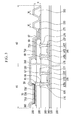
- FIG. 3 is a cross-sectional view taken along line III-III of FIG. 1 , according to an exemplary embodiment of the present invention.
- FIG. 4 is a cross-sectional view of an organic light emitting diode (OLED) display, according to an exemplary embodiment of the present invention.
- OLED organic light emitting diode
- FIG. 3 illustrates a pixel PX according to a layer lamination order focusing on the driving thin film transistor Qd and the organic light emitting element 70 of FIG. 1 .
- the built-in circuit unit DA1 of the peripheral area A2 may include a thin film transistor having various shapes and sizes according to the circuit, and it is to be understood that exemplary embodiments are not limited to the thin film transistor as described herein.
- the driving thin film transistor Qd positioned at the pixel area A1 may be referred to as a pixel thin film transistor
- the thin film transistor of the built-in circuit unit DA1 positioned at the peripheral area A2 may be referred to as a peripheral thin film transistor.
- the organic light emitting diode (OLED) display includes a substrate 100.
- a buffer layer 120 may be formed on the substrate 100.
- the substrate 100 may be a transparent insulating substrate made of, for example, glass, quartz, ceramic, or plastic, or a metal substrate made of, for example, stainless steel.
- the buffer layer 120 may be a single layer buffer layer or a multi-layer buffer layer.
- the buffer layer 120 may be formed of a single layer of a silicon nitride (SiNx), or a multi-layer in which a silicon nitride (SiNx) and a silicon oxide (SiO x ) are deposited.
- the buffer layer 120 may prevent impurities or moisture from infiltrating the substrate 100, and may planarize the surface of the substrate 100.
- Semiconductor layers 135 and 145 may be formed on the buffer layer 120 and may be formed of, for example, polysilicon.
- the semiconductor layers 135 and 145 are respectively divided into channel regions 1355 and 1455, and source regions 1356 and 1456 and drain regions 1357 and 1457 may be formed on respective sides of the channel regions 1355 and 1455.
- the channel regions 1355 and 1455 may be made of, for example, undoped polysilicon (e.g., an intrinsic semiconductor).
- the source regions 1356 and 1456 and the drain regions 1357 and 1457 may be made of, for example, polysilicon doped with a conductive impurity (e.g., an impurity semiconductor).
- the impurity doped into the source regions 1356 and 1456 and the drain regions 1357 and 1457 may be, for example, a p-type impurity or an n-type impurity.
- a gate insulating layer 140 is formed on the semiconductor layers 135 and 145.
- the gate insulating layer 140 may be a single layer or a multi-layer including at least one of tetraethyl orthosilicate (TEOS), a silicon nitride, and a silicon oxide.
- TEOS tetraethyl orthosilicate
- Gate electrodes 155 and 157 are formed on the gate insulating layer 140 and the gate electrodes 155 and 157 respectively overlap the channel regions 1355 and 1455.
- the gate electrodes 155 and 157 may be formed of a single layer or multiple layers of a low resistance material or a highly corrosion-resistant material such as, for example, A1, Ti, Mo, Cu, Ni, and alloys thereof.
- a first interlayer insulating layer 160 is formed on the gate electrodes 155 and 157.
- the first interlayer insulating layer 160 may be formed of a single layer or multiple layers including at least one of tetraethyl orthosilicate (TEOS), a silicon nitride, and a silicon oxide.
- TEOS tetraethyl orthosilicate
- silicon nitride silicon nitride
- the first interlayer insulating layer 160 and the gate insulating layer 140 include source contact holes 66 and 68 and drain contact holes 67 and 69, which respectively expose the source regions 1356 and 1456 and the drain regions 1357 and 1457.
- Source electrodes 176 and 178 and drain electrodes 177 and 179, and a common voltage line 173 are formed on the first interlayer insulating layer 160.
- the source electrodes 176 and 178 and the drain electrodes 177 and 179 are respectively connected to the source regions 1356 and 1456 and the drain regions 1357 and 1457 through the contact holes 66, 68, 67, and 69.
- the drain electrodes 177 and 179 may be made of single or multiple layers of a low resistance material or a highly corrosion-resistant material such as, for example, A1, Ti, Mo, Cu, Ni, and alloys thereof.
- the drain electrodes 177 and 179 may be formed of three-level layers of Ti/Cu/Ti, Ti/Ag/Ti, or Mo/Al/Mo.
- the gate electrode 155, the source electrode 176, and the drain electrode 177 function as the control electrode, the input electrode, and the output electrode of FIG. 2 and form the pixel thin film transistor along the semiconductor layer 135.
- the gate electrode 157, the source electrode 178 and drain electrode 179 form the peripheral thin film transistor along with the semiconductor layer 145.
- the channel of the thin film transistor is respectively formed at the semiconductor layers 135 and 145 between the source electrodes 176 and 178 and the drain electrodes 177 and 179.
- a second interlayer insulating layer 180 and a first protection member 183 are formed on the source electrodes 176 and 178 and the drain electrodes 177 and 179.
- the second interlayer insulating layer 180 may be formed of a single layer or multiple layers of at least one of tetraethyl orthosilicate (TEOS), a silicon nitride, and a silicon oxide.
- TEOS tetraethyl orthosilicate
- the second interlayer insulating layer 180 may be formed of a low dielectric constant organic material.
- the second interlayer insulating layer 180 includes a contact hole 85 exposing the drain electrode 177.
- An end of the second interlayer insulating layer 180 is positioned on the common voltage line 173, thereby covering one side of the common voltage line 173.
- the first protection member 183 overlaps the common voltage line 173 and encloses the pixel area A1 according to the layout of the common voltage line, thereby covering the other side of the common voltage line 173 (e.g., covering the side of the common voltage line 173 disposed in the peripheral area A2 on the opposing side of the pixel area A1).
- the first protection member 183 may be formed with the same material as the second interlayer insulating layer 180.
- the first protection member 183 forms an opening 87 exposing the common voltage line 173 when forming the contact hole 85 after forming the second interlayer insulating layer 180, thereby forming the first protection member 183 separated from the second interlayer insulating layer 180.
- a first electrode 710 and a connection member 733 are formed on the second interlayer insulating layer 180.
- the first electrode 710 may be an anode of the organic light emitting element 70 of FIG. 2 .
- the second interlayer insulating layer 180 is formed between the first electrode 710 and the drain electrode 177.
- the first electrode 710 may be formed of the same material as the drain electrode 177, and may be integrally formed with the drain electrode 177.
- connection member 733 contacts the common voltage line 173 exposed through the opening 87, and is electrically connected thereto.
- a barrier rib 190 and a second protection member 193 are formed on the first electrode 710.
- the barrier rib 190 includes an opening 95 exposing the first electrode 710.
- the barrier rib 190 may include a polyacrylate or polyimide resin and a silica-based inorganic material.
- the second protection member 193 covers and protects one side of the connection member 733 overlapping the common voltage line 173.
- the first and second protection members 183 and 193 may cover one side of the common voltage line 173, and the barrier rib 190 may cover the other side of the common voltage line 173 (e.g., the side of the common voltage line 173 disposed in the peripheral area A2 on the opposing side of the pixel area A1).
- a space between the first protection member 183 and the second protection member 193 may be more than about 10 ⁇ m. When the space between the first protection member 183 and the second protection member 193 is narrow, an overlying layer may not be formed between the first protection member 183 and the second protection member 193.
- the first protection member 183 may be formed along with the second interlayer insulating layer 180, and the first protection member 183 may be formed with the same material as the second protection member 193.
- the first protection member 183 and the second protection member 193 may be formed together.
- the first and second protection members 183 and 193 may form the barrier rib 190.
- the first protection member 183 and the second protection member 193 may be formed as one protection member 903 as shown in the exemplary embodiment of FIG. 4 . That is, the exemplary embodiment of FIG. 3 may include first and second protection members 183 and 193, and the exemplary embodiment of FIG. 4 may include one protection member 903.
- the barrier rib 190 may be described as including a first opening 95 exposing the first electrode 710, and a second opening 87 exposing the common voltage line 173. As shown in FIGs. 3 and 4 , a boundary of the second opening 87 may be positioned within a boundary of the common voltage line 173. That is, the boundary of the second opening 87 may overlap a side of the common voltage line 173.
- a thickness H of the first protection member 183 may be greater than a thickness of the common voltage line 173. As a result, the first protection member 183 may completely cover a side wall of the common voltage line 173.
- the thickness H of the first protection member 183 may be less than about 1.5 ⁇ m, and a width W of the first protection member 183 may be in a range from about 10 ⁇ m to about 30 ⁇ m.
- an organic emission layer 720 may be formed in the opening 95 of the barrier rib 190.
- the thickness H and width W of the first and second protection members 183 and 193 may be the same, or substantially the same.
- the organic emission layer 720 may be formed of multiple layers including an emission layer and one or more of a hole injection layer (HIL), a hole transport layer (HTL), an electron transport layer (ETL), and an electron injection layer (EIL).
- HIL hole injection layer
- HTL hole transport layer
- ETL electron transport layer
- EIL electron injection layer
- the hole injection layer may be disposed on the first electrode 710 corresponding to the anode, and the hole transport layer, the emission layer, the electron transport layer, and the electron injection layer may be sequentially laminated on the hole injection layer.
- a second electrode 730 may be formed on the connection member 733, the barrier rib 190, and the organic emission layer 720.
- the second electrode 730 may be a cathode of the organic light emitting element 70. Accordingly, the first electrode 710, the organic emission layer 720, and the second electrode 730 form the organic light emitting element 70.
- the organic light emitting element 70 may be of one of a front display type, a rear display type, and a dual-sided display type according to the direction in which the organic light-emitting element 70 emits light.
- the first electrode 710 may be formed of a reflective layer and the second electrode 730 may be formed of a transflective or transmissive layer.
- the first electrode 710 may be formed of a transflective layer and the second electrode 730 may be formed of a reflective layer.
- the first electrode 710 and the second electrode 730 may be formed of a transparent layer or a semi-transparent layer.
- the reflective layer and the semi-transparent layer are made of at least one of Mg, Ag, Au, Ca, Li, Cr, and Al, or an alloy thereof.
- the reflective layer and the transflective layer are determined by the thicknesses thereof, and the transflective layer may have a thickness of less than about 200 nm. While the transmittance of the reflective layer or transflective layer may increase as the thickness thereof decreases, the resistance thereof may increase when the layer is excessively thin.
- the transmissive layer is made of indium tin oxide (ITO), indium zinc oxide (IZO), zinc oxide (ZnO), or indium oxide (In 2 O 3 ).
- the second electrode 730 is connected to the common voltage line 173 via the connection member 733, thereby receiving the signal. Accordingly, a voltage drop of the second electrode 730 may be prevented by the common voltage line 173.
- An encapsulation layer 260 is formed on the second electrode 730.
- the encapsulation layer 260 may be formed by alternately forming at least one organic layer and at least one inorganic layer. A plurality of organic layers or a plurality of inorganic layers may be formed.
- the organic layer is formed of a polymer, and may be a single layer or a deposition layer including one of polyethylene terephthalate, a polyimide, a polycarbonate, an epoxy, polyethylene, and a polyacrylate. Further, the organic layer may be formed with a polyacrylate, and may include a polymerized monomer composition including a diacrylate monomer and triacrylate monomer. A monoacrylate monomer may be included in the monomer composition. A photoinitiator such as TPO may be further included in the monomer composition, however, exemplary embodiments are not limited thereto.
- the inorganic layer may be a single layer or a deposition layer including a metal oxide or a metal nitride.
- the inorganic layer may include, for example, one of SiNx, Al2O3, SiO2, and TiO2.
- the externally exposed uppermost layer of the encapsulation layer 260 may be formed with an inorganic layer. As a result, permeation of vapor into the organic light emitting element may be reduced or prevented.
- the encapsulation layer 260 may include at least one sandwich configuration in which at least one organic layer is disposed between at least two inorganic layers, or in which at least one inorganic layer is disposed between at least two organic layers.
- the encapsulation layer 260 may sequentially include a first inorganic layer, a first organic layer, and a second inorganic layer disposed in order from top to bottom of the OLED display.
- the encapsulation layer 260 may sequentially include a first inorganic layer, a first organic layer, a second inorganic layer, a second organic layer, and a third inorganic layer disposed in order from top to bottom of the OLED display.
- the encapsulation layer 260 may sequentially include a first inorganic layer, a first organic layer, a second inorganic layer, a second organic layer, a third inorganic layer, a third organic layer, and a fourth inorganic layer disposed in order from top to bottom of the OLED display.
- a metal halide layer including LiF may be included between an upper portion of the OLED display and the first inorganic layer.
- the metal halide layer may prevent the OLED display from being damaged when the first inorganic layer is formed using, for example, a sputtering method or a plasma deposition method.
- the first organic layer may be narrower than the second inorganic layer, and the second organic layer may be narrower than the third inorganic layer. Further, the first organic layer may be covered (e.g., entirely covered) by the second inorganic layer, and the second organic layer may be covered (e.g., entirely covered) by the third inorganic layer.
- the side wall of the common voltage line 173 may be prevented from being exposed by the first protection member 183, and a disconnection of the encapsulation layer 260 by the side wall of the common voltage line 173 may be prevented.
- the side wall of the common voltage line 173 may be damaged during a following process.
- the side wall is protected by the first protection member 183 such that damage may be prevented, even if the side wall is exposed during a following process.
- an undercut may be generated by an etching difference.
- the overlying layer may not be formed according to the side wall of the common voltage line 173 and may be disconnected by this undercut.
- the first protection member 183 may cover the undercut such that a side wall having a substantially smooth inclination is formed.
- the overlying layer such as, for example, the encapsulation layer 260, may be formed according to the layout of the side wall without a disconnection occurring.
Landscapes
- Engineering & Computer Science (AREA)
- Microelectronics & Electronic Packaging (AREA)
- Physics & Mathematics (AREA)
- Optics & Photonics (AREA)
- Manufacturing & Machinery (AREA)
- Electroluminescent Light Sources (AREA)
- Devices For Indicating Variable Information By Combining Individual Elements (AREA)
Applications Claiming Priority (1)
| Application Number | Priority Date | Filing Date | Title |
|---|---|---|---|
| KR1020130094305A KR102158771B1 (ko) | 2013-08-08 | 2013-08-08 | 유기 발광 표시 장치 |
Publications (3)
| Publication Number | Publication Date |
|---|---|
| EP2835831A2 true EP2835831A2 (fr) | 2015-02-11 |
| EP2835831A3 EP2835831A3 (fr) | 2015-03-18 |
| EP2835831B1 EP2835831B1 (fr) | 2019-05-08 |
Family
ID=51300573
Family Applications (1)
| Application Number | Title | Priority Date | Filing Date |
|---|---|---|---|
| EP14180162.1A Active EP2835831B1 (fr) | 2013-08-08 | 2014-08-07 | Affichage à diodes électroluminescentes organiques |
Country Status (3)
| Country | Link |
|---|---|
| US (1) | US9466810B2 (fr) |
| EP (1) | EP2835831B1 (fr) |
| KR (1) | KR102158771B1 (fr) |
Cited By (3)
| Publication number | Priority date | Publication date | Assignee | Title |
|---|---|---|---|---|
| CN110911461A (zh) * | 2019-11-26 | 2020-03-24 | 深圳市华星光电半导体显示技术有限公司 | Oled显示面板及其制作方法 |
| CN115036352A (zh) * | 2015-05-01 | 2022-09-09 | 三星显示有限公司 | 有机发光设备及其制造方法 |
| EP4044244A4 (fr) * | 2020-06-30 | 2022-11-23 | BOE Technology Group Co., Ltd. | Panneau d'affichage et dispositif d'affichage |
Families Citing this family (27)
| Publication number | Priority date | Publication date | Assignee | Title |
|---|---|---|---|---|
| CN104393188A (zh) * | 2014-11-28 | 2015-03-04 | 京东方科技集团股份有限公司 | 一种有机发光二极管显示基板及其制作方法、显示装置 |
| KR102314470B1 (ko) * | 2015-03-09 | 2021-10-20 | 삼성디스플레이 주식회사 | 유기 발광 표시 장치 |
| KR102477299B1 (ko) | 2015-06-12 | 2022-12-14 | 삼성디스플레이 주식회사 | 디스플레이 장치 |
| KR101763616B1 (ko) | 2015-07-29 | 2017-08-02 | 삼성디스플레이 주식회사 | 유기 발광 표시 장치 |
| KR102446425B1 (ko) * | 2015-11-17 | 2022-09-23 | 삼성디스플레이 주식회사 | 표시 장치 및 표시 장치의 제조 방법 |
| KR102571085B1 (ko) | 2016-04-04 | 2023-08-28 | 삼성디스플레이 주식회사 | 디스플레이 장치 |
| CN107403817B (zh) * | 2016-05-20 | 2020-06-23 | 群创光电股份有限公司 | 显示装置 |
| US10490534B2 (en) * | 2016-05-20 | 2019-11-26 | Innolux Corporation | Display device with LED pixels |
| KR102404573B1 (ko) * | 2016-05-27 | 2022-06-03 | 삼성디스플레이 주식회사 | 디스플레이 장치 |
| KR102632616B1 (ko) * | 2016-06-27 | 2024-02-02 | 삼성디스플레이 주식회사 | 디스플레이 장치 |
| KR102656842B1 (ko) * | 2016-10-24 | 2024-04-17 | 엘지디스플레이 주식회사 | 플렉서블 표시장치 |
| KR102594921B1 (ko) * | 2016-10-31 | 2023-10-26 | 엘지디스플레이 주식회사 | 유기 발광 표시 장치 |
| KR102328679B1 (ko) | 2016-11-23 | 2021-11-19 | 삼성디스플레이 주식회사 | 표시 장치 |
| WO2019025910A1 (fr) * | 2017-08-04 | 2019-02-07 | Semiconductor Energy Laboratory Co., Ltd. | Panneau d'affichage, dispositif d'affichage, module d'affichage, et dispositif électronique |
| TWI634468B (zh) * | 2017-08-18 | 2018-09-01 | Industrial Technology Research Institute | 透明顯示裝置 |
| CN108010941B (zh) * | 2017-11-15 | 2020-08-11 | 纳晶科技股份有限公司 | 用于发光元件的封装结构及方法 |
| US11765941B2 (en) * | 2017-12-26 | 2023-09-19 | Sharp Kabushiki Kaisha | Display device |
| CN109004093B (zh) * | 2018-07-13 | 2020-07-07 | 京东方科技集团股份有限公司 | Oled面板及其制造方法、电子设备 |
| KR102684270B1 (ko) * | 2018-10-05 | 2024-07-12 | 삼성디스플레이 주식회사 | 디스플레이 장치 |
| KR102885297B1 (ko) | 2019-01-11 | 2025-11-12 | 삼성디스플레이 주식회사 | 유기 발광 표시 장치 |
| CN110600528A (zh) * | 2019-10-08 | 2019-12-20 | 昆山国显光电有限公司 | 显示面板和显示装置 |
| KR102895954B1 (ko) * | 2019-10-17 | 2025-12-04 | 삼성디스플레이 주식회사 | 표시장치 |
| KR102761120B1 (ko) * | 2019-12-11 | 2025-01-31 | 엘지디스플레이 주식회사 | 표시장치 |
| KR102894386B1 (ko) | 2021-02-19 | 2025-12-02 | 삼성디스플레이 주식회사 | 표시 장치 |
| KR102890699B1 (ko) * | 2021-09-23 | 2025-11-25 | 삼성디스플레이 주식회사 | 표시 장치 및 그 표시 장치의 제조 방법 |
| CN114203785B (zh) | 2021-12-10 | 2023-05-09 | 武汉华星光电半导体显示技术有限公司 | 一种oled显示面板 |
| CN114975554B (zh) * | 2022-05-26 | 2025-05-27 | 深圳市华星光电半导体显示技术有限公司 | 双面显示面板及移动终端 |
Family Cites Families (15)
| Publication number | Priority date | Publication date | Assignee | Title |
|---|---|---|---|---|
| AU2003260959A1 (en) * | 2002-09-11 | 2004-04-30 | Semiconductor Energy Laboratory Co., Ltd. | Light-emitting apparatus and fabrication method of the same |
| US7710019B2 (en) * | 2002-12-11 | 2010-05-04 | Samsung Electronics Co., Ltd. | Organic light-emitting diode display comprising auxiliary electrodes |
| KR100553745B1 (ko) | 2003-08-06 | 2006-02-20 | 삼성에스디아이 주식회사 | 평판표시장치 |
| US7538488B2 (en) * | 2004-02-14 | 2009-05-26 | Samsung Mobile Display Co., Ltd. | Flat panel display |
| KR100581903B1 (ko) * | 2004-03-09 | 2006-05-22 | 삼성에스디아이 주식회사 | 전계 발광 디스플레이 장치 |
| KR101141650B1 (ko) | 2004-09-30 | 2012-05-17 | 엘지전자 주식회사 | 매체접속제어 계층에서의 데이터 처리 방법 및 이동통신용단말 |
| US7692377B2 (en) * | 2005-11-16 | 2010-04-06 | Canon Kabushiki Kaisha | Light emitting display device provided with external connection terminal located at peripheral portions of a display area |
| JP5119865B2 (ja) * | 2007-11-02 | 2013-01-16 | セイコーエプソン株式会社 | 有機エレクトロルミネッセンス装置、電子機器 |
| KR20110019498A (ko) | 2009-08-20 | 2011-02-28 | 삼성모바일디스플레이주식회사 | 유기전계발광 표시장치 |
| KR101889918B1 (ko) * | 2010-12-14 | 2018-09-21 | 삼성디스플레이 주식회사 | 유기 발광 디스플레이 장치 및 이의 제조 방법 |
| KR101984309B1 (ko) | 2010-12-20 | 2019-05-30 | 가부시키가이샤 재팬 디스프레이 | 화소 구조, 표시 장치, 및 전자 기기 |
| KR102004305B1 (ko) * | 2011-02-11 | 2019-07-26 | 가부시키가이샤 한도오따이 에네루기 켄큐쇼 | 발광 장치 및 그 제작 방법, 그리고 조명 장치 및 표시 장치 |
| KR101463650B1 (ko) * | 2011-08-30 | 2014-11-20 | 엘지디스플레이 주식회사 | 유기발광표시장치 및 그 제조방법 |
| JP6135062B2 (ja) * | 2012-08-07 | 2017-05-31 | セイコーエプソン株式会社 | 発光装置、発光装置の製造方法、電子機器 |
| KR102013319B1 (ko) * | 2013-05-30 | 2019-11-05 | 삼성디스플레이 주식회사 | 평판 표시 장치 및 이의 제조 방법 |
-
2013
- 2013-08-08 KR KR1020130094305A patent/KR102158771B1/ko active Active
-
2014
- 2014-08-04 US US14/450,369 patent/US9466810B2/en active Active
- 2014-08-07 EP EP14180162.1A patent/EP2835831B1/fr active Active
Non-Patent Citations (1)
| Title |
|---|
| None |
Cited By (4)
| Publication number | Priority date | Publication date | Assignee | Title |
|---|---|---|---|---|
| CN115036352A (zh) * | 2015-05-01 | 2022-09-09 | 三星显示有限公司 | 有机发光设备及其制造方法 |
| CN110911461A (zh) * | 2019-11-26 | 2020-03-24 | 深圳市华星光电半导体显示技术有限公司 | Oled显示面板及其制作方法 |
| EP4044244A4 (fr) * | 2020-06-30 | 2022-11-23 | BOE Technology Group Co., Ltd. | Panneau d'affichage et dispositif d'affichage |
| US11871626B2 (en) | 2020-06-30 | 2024-01-09 | Chengdu Boe Optoelectronics Technology Co., Ltd. | Display panel and display device |
Also Published As
| Publication number | Publication date |
|---|---|
| KR102158771B1 (ko) | 2020-09-23 |
| KR20150017978A (ko) | 2015-02-23 |
| EP2835831B1 (fr) | 2019-05-08 |
| US20150041791A1 (en) | 2015-02-12 |
| EP2835831A3 (fr) | 2015-03-18 |
| US9466810B2 (en) | 2016-10-11 |
Similar Documents
| Publication | Publication Date | Title |
|---|---|---|
| EP2835831B1 (fr) | Affichage à diodes électroluminescentes organiques | |
| US10937838B2 (en) | Organic light emitting display device | |
| US9064833B2 (en) | Organic light emitting diode display | |
| US10204846B2 (en) | Display device | |
| KR102724697B1 (ko) | 표시 장치 및 가요성 표시 장치 | |
| CN112385313B (zh) | 显示设备 | |
| US12262601B2 (en) | Light emitting display device and manufacturing method thereof | |
| US10665820B2 (en) | Display device | |
| US11574975B2 (en) | Light emitting diode display device with channel region covered by drain electrode | |
| KR100879294B1 (ko) | 유기 발광 표시 장치 | |
| US7772764B2 (en) | Display device and method of manufacturing the same | |
| KR20160116248A (ko) | 표시 장치 및 그 제조 방법 | |
| KR102515631B1 (ko) | 유기 발광 표시 장치 | |
| CN114695470A (zh) | 显示装置 | |
| KR102247825B1 (ko) | 칼라 필터를 구비한 하부 발광형 유기발광 다이오드 표시장치 및 그 제조 방법 | |
| US20250393426A1 (en) | Organic light-emitting display device including conductive lines having inclined surface | |
| US20240244893A1 (en) | Display Device | |
| KR20210074549A (ko) | 유기발광 표시장치 | |
| KR20220091134A (ko) | 표시 패널 | |
| KR102863290B1 (ko) | 유기 발광 표시 장치 | |
| US20240334784A1 (en) | Display Apparatus | |
| US20240081121A1 (en) | Display device | |
| KR102789541B1 (ko) | 유기발광 표시장치 | |
| CN111133496A (zh) | 显示设备、显示设备的制造方法、显示设备的制造装置 |
Legal Events
| Date | Code | Title | Description |
|---|---|---|---|
| PUAI | Public reference made under article 153(3) epc to a published international application that has entered the european phase |
Free format text: ORIGINAL CODE: 0009012 |
|
| 17P | Request for examination filed |
Effective date: 20140807 |
|
| AK | Designated contracting states |
Kind code of ref document: A2 Designated state(s): AL AT BE BG CH CY CZ DE DK EE ES FI FR GB GR HR HU IE IS IT LI LT LU LV MC MK MT NL NO PL PT RO RS SE SI SK SM TR |
|
| AX | Request for extension of the european patent |
Extension state: BA ME |
|
| PUAL | Search report despatched |
Free format text: ORIGINAL CODE: 0009013 |
|
| AK | Designated contracting states |
Kind code of ref document: A3 Designated state(s): AL AT BE BG CH CY CZ DE DK EE ES FI FR GB GR HR HU IE IS IT LI LT LU LV MC MK MT NL NO PL PT RO RS SE SI SK SM TR |
|
| AX | Request for extension of the european patent |
Extension state: BA ME |
|
| RIC1 | Information provided on ipc code assigned before grant |
Ipc: H01L 27/32 20060101AFI20150211BHEP |
|
| R17P | Request for examination filed (corrected) |
Effective date: 20150519 |
|
| RBV | Designated contracting states (corrected) |
Designated state(s): AL AT BE BG CH CY CZ DE DK EE ES FI FR GB GR HR HU IE IS IT LI LT LU LV MC MK MT NL NO PL PT RO RS SE SI SK SM TR |
|
| RAP1 | Party data changed (applicant data changed or rights of an application transferred) |
Owner name: SAMSUNG DISPLAY CO., LTD. |
|
| 17Q | First examination report despatched |
Effective date: 20160715 |
|
| STAA | Information on the status of an ep patent application or granted ep patent |
Free format text: STATUS: EXAMINATION IS IN PROGRESS |
|
| GRAP | Despatch of communication of intention to grant a patent |
Free format text: ORIGINAL CODE: EPIDOSNIGR1 |
|
| STAA | Information on the status of an ep patent application or granted ep patent |
Free format text: STATUS: GRANT OF PATENT IS INTENDED |
|
| RIC1 | Information provided on ipc code assigned before grant |
Ipc: H01L 27/32 20060101AFI20181114BHEP Ipc: H01L 27/12 20060101ALI20181114BHEP |
|
| INTG | Intention to grant announced |
Effective date: 20181129 |
|
| RIN1 | Information on inventor provided before grant (corrected) |
Inventor name: JAE-YONG, LEE Inventor name: YANG-WAN, KIM |
|
| GRAS | Grant fee paid |
Free format text: ORIGINAL CODE: EPIDOSNIGR3 |
|
| GRAA | (expected) grant |
Free format text: ORIGINAL CODE: 0009210 |
|
| STAA | Information on the status of an ep patent application or granted ep patent |
Free format text: STATUS: THE PATENT HAS BEEN GRANTED |
|
| AK | Designated contracting states |
Kind code of ref document: B1 Designated state(s): AL AT BE BG CH CY CZ DE DK EE ES FI FR GB GR HR HU IE IS IT LI LT LU LV MC MK MT NL NO PL PT RO RS SE SI SK SM TR |
|
| REG | Reference to a national code |
Ref country code: GB Ref legal event code: FG4D |
|
| REG | Reference to a national code |
Ref country code: CH Ref legal event code: EP Ref country code: AT Ref legal event code: REF Ref document number: 1131577 Country of ref document: AT Kind code of ref document: T Effective date: 20190515 |
|
| REG | Reference to a national code |
Ref country code: IE Ref legal event code: FG4D |
|
| REG | Reference to a national code |
Ref country code: DE Ref legal event code: R096 Ref document number: 602014046164 Country of ref document: DE |
|
| REG | Reference to a national code |
Ref country code: NL Ref legal event code: MP Effective date: 20190508 |
|
| REG | Reference to a national code |
Ref country code: LT Ref legal event code: MG4D |
|
| PG25 | Lapsed in a contracting state [announced via postgrant information from national office to epo] |
Ref country code: FI Free format text: LAPSE BECAUSE OF FAILURE TO SUBMIT A TRANSLATION OF THE DESCRIPTION OR TO PAY THE FEE WITHIN THE PRESCRIBED TIME-LIMIT Effective date: 20190508 Ref country code: NO Free format text: LAPSE BECAUSE OF FAILURE TO SUBMIT A TRANSLATION OF THE DESCRIPTION OR TO PAY THE FEE WITHIN THE PRESCRIBED TIME-LIMIT Effective date: 20190808 Ref country code: HR Free format text: LAPSE BECAUSE OF FAILURE TO SUBMIT A TRANSLATION OF THE DESCRIPTION OR TO PAY THE FEE WITHIN THE PRESCRIBED TIME-LIMIT Effective date: 20190508 Ref country code: LT Free format text: LAPSE BECAUSE OF FAILURE TO SUBMIT A TRANSLATION OF THE DESCRIPTION OR TO PAY THE FEE WITHIN THE PRESCRIBED TIME-LIMIT Effective date: 20190508 Ref country code: NL Free format text: LAPSE BECAUSE OF FAILURE TO SUBMIT A TRANSLATION OF THE DESCRIPTION OR TO PAY THE FEE WITHIN THE PRESCRIBED TIME-LIMIT Effective date: 20190508 Ref country code: ES Free format text: LAPSE BECAUSE OF FAILURE TO SUBMIT A TRANSLATION OF THE DESCRIPTION OR TO PAY THE FEE WITHIN THE PRESCRIBED TIME-LIMIT Effective date: 20190508 Ref country code: PT Free format text: LAPSE BECAUSE OF FAILURE TO SUBMIT A TRANSLATION OF THE DESCRIPTION OR TO PAY THE FEE WITHIN THE PRESCRIBED TIME-LIMIT Effective date: 20190908 Ref country code: AL Free format text: LAPSE BECAUSE OF FAILURE TO SUBMIT A TRANSLATION OF THE DESCRIPTION OR TO PAY THE FEE WITHIN THE PRESCRIBED TIME-LIMIT Effective date: 20190508 Ref country code: SE Free format text: LAPSE BECAUSE OF FAILURE TO SUBMIT A TRANSLATION OF THE DESCRIPTION OR TO PAY THE FEE WITHIN THE PRESCRIBED TIME-LIMIT Effective date: 20190508 |
|
| PG25 | Lapsed in a contracting state [announced via postgrant information from national office to epo] |
Ref country code: GR Free format text: LAPSE BECAUSE OF FAILURE TO SUBMIT A TRANSLATION OF THE DESCRIPTION OR TO PAY THE FEE WITHIN THE PRESCRIBED TIME-LIMIT Effective date: 20190809 Ref country code: LV Free format text: LAPSE BECAUSE OF FAILURE TO SUBMIT A TRANSLATION OF THE DESCRIPTION OR TO PAY THE FEE WITHIN THE PRESCRIBED TIME-LIMIT Effective date: 20190508 Ref country code: RS Free format text: LAPSE BECAUSE OF FAILURE TO SUBMIT A TRANSLATION OF THE DESCRIPTION OR TO PAY THE FEE WITHIN THE PRESCRIBED TIME-LIMIT Effective date: 20190508 Ref country code: BG Free format text: LAPSE BECAUSE OF FAILURE TO SUBMIT A TRANSLATION OF THE DESCRIPTION OR TO PAY THE FEE WITHIN THE PRESCRIBED TIME-LIMIT Effective date: 20190808 |
|
| REG | Reference to a national code |
Ref country code: AT Ref legal event code: MK05 Ref document number: 1131577 Country of ref document: AT Kind code of ref document: T Effective date: 20190508 |
|
| PG25 | Lapsed in a contracting state [announced via postgrant information from national office to epo] |
Ref country code: RO Free format text: LAPSE BECAUSE OF FAILURE TO SUBMIT A TRANSLATION OF THE DESCRIPTION OR TO PAY THE FEE WITHIN THE PRESCRIBED TIME-LIMIT Effective date: 20190508 Ref country code: SK Free format text: LAPSE BECAUSE OF FAILURE TO SUBMIT A TRANSLATION OF THE DESCRIPTION OR TO PAY THE FEE WITHIN THE PRESCRIBED TIME-LIMIT Effective date: 20190508 Ref country code: CZ Free format text: LAPSE BECAUSE OF FAILURE TO SUBMIT A TRANSLATION OF THE DESCRIPTION OR TO PAY THE FEE WITHIN THE PRESCRIBED TIME-LIMIT Effective date: 20190508 Ref country code: DK Free format text: LAPSE BECAUSE OF FAILURE TO SUBMIT A TRANSLATION OF THE DESCRIPTION OR TO PAY THE FEE WITHIN THE PRESCRIBED TIME-LIMIT Effective date: 20190508 Ref country code: AT Free format text: LAPSE BECAUSE OF FAILURE TO SUBMIT A TRANSLATION OF THE DESCRIPTION OR TO PAY THE FEE WITHIN THE PRESCRIBED TIME-LIMIT Effective date: 20190508 Ref country code: EE Free format text: LAPSE BECAUSE OF FAILURE TO SUBMIT A TRANSLATION OF THE DESCRIPTION OR TO PAY THE FEE WITHIN THE PRESCRIBED TIME-LIMIT Effective date: 20190508 |
|
| REG | Reference to a national code |
Ref country code: DE Ref legal event code: R097 Ref document number: 602014046164 Country of ref document: DE |
|
| PG25 | Lapsed in a contracting state [announced via postgrant information from national office to epo] |
Ref country code: IT Free format text: LAPSE BECAUSE OF FAILURE TO SUBMIT A TRANSLATION OF THE DESCRIPTION OR TO PAY THE FEE WITHIN THE PRESCRIBED TIME-LIMIT Effective date: 20190508 Ref country code: SM Free format text: LAPSE BECAUSE OF FAILURE TO SUBMIT A TRANSLATION OF THE DESCRIPTION OR TO PAY THE FEE WITHIN THE PRESCRIBED TIME-LIMIT Effective date: 20190508 |
|
| PLBE | No opposition filed within time limit |
Free format text: ORIGINAL CODE: 0009261 |
|
| STAA | Information on the status of an ep patent application or granted ep patent |
Free format text: STATUS: NO OPPOSITION FILED WITHIN TIME LIMIT |
|
| PG25 | Lapsed in a contracting state [announced via postgrant information from national office to epo] |
Ref country code: TR Free format text: LAPSE BECAUSE OF FAILURE TO SUBMIT A TRANSLATION OF THE DESCRIPTION OR TO PAY THE FEE WITHIN THE PRESCRIBED TIME-LIMIT Effective date: 20190508 |
|
| 26N | No opposition filed |
Effective date: 20200211 |
|
| PG25 | Lapsed in a contracting state [announced via postgrant information from national office to epo] |
Ref country code: PL Free format text: LAPSE BECAUSE OF FAILURE TO SUBMIT A TRANSLATION OF THE DESCRIPTION OR TO PAY THE FEE WITHIN THE PRESCRIBED TIME-LIMIT Effective date: 20190508 |
|
| PG25 | Lapsed in a contracting state [announced via postgrant information from national office to epo] |
Ref country code: CH Free format text: LAPSE BECAUSE OF NON-PAYMENT OF DUE FEES Effective date: 20190831 Ref country code: MC Free format text: LAPSE BECAUSE OF FAILURE TO SUBMIT A TRANSLATION OF THE DESCRIPTION OR TO PAY THE FEE WITHIN THE PRESCRIBED TIME-LIMIT Effective date: 20190508 Ref country code: LU Free format text: LAPSE BECAUSE OF NON-PAYMENT OF DUE FEES Effective date: 20190807 Ref country code: LI Free format text: LAPSE BECAUSE OF NON-PAYMENT OF DUE FEES Effective date: 20190831 Ref country code: SI Free format text: LAPSE BECAUSE OF FAILURE TO SUBMIT A TRANSLATION OF THE DESCRIPTION OR TO PAY THE FEE WITHIN THE PRESCRIBED TIME-LIMIT Effective date: 20190508 |
|
| REG | Reference to a national code |
Ref country code: BE Ref legal event code: MM Effective date: 20190831 |
|
| PG25 | Lapsed in a contracting state [announced via postgrant information from national office to epo] |
Ref country code: IE Free format text: LAPSE BECAUSE OF NON-PAYMENT OF DUE FEES Effective date: 20190807 |
|
| PG25 | Lapsed in a contracting state [announced via postgrant information from national office to epo] |
Ref country code: BE Free format text: LAPSE BECAUSE OF NON-PAYMENT OF DUE FEES Effective date: 20190831 |
|
| PG25 | Lapsed in a contracting state [announced via postgrant information from national office to epo] |
Ref country code: CY Free format text: LAPSE BECAUSE OF FAILURE TO SUBMIT A TRANSLATION OF THE DESCRIPTION OR TO PAY THE FEE WITHIN THE PRESCRIBED TIME-LIMIT Effective date: 20190508 |
|
| PG25 | Lapsed in a contracting state [announced via postgrant information from national office to epo] |
Ref country code: IS Free format text: LAPSE BECAUSE OF FAILURE TO SUBMIT A TRANSLATION OF THE DESCRIPTION OR TO PAY THE FEE WITHIN THE PRESCRIBED TIME-LIMIT Effective date: 20190908 |
|
| PG25 | Lapsed in a contracting state [announced via postgrant information from national office to epo] |
Ref country code: HU Free format text: LAPSE BECAUSE OF FAILURE TO SUBMIT A TRANSLATION OF THE DESCRIPTION OR TO PAY THE FEE WITHIN THE PRESCRIBED TIME-LIMIT; INVALID AB INITIO Effective date: 20140807 Ref country code: MT Free format text: LAPSE BECAUSE OF FAILURE TO SUBMIT A TRANSLATION OF THE DESCRIPTION OR TO PAY THE FEE WITHIN THE PRESCRIBED TIME-LIMIT Effective date: 20190508 |
|
| PG25 | Lapsed in a contracting state [announced via postgrant information from national office to epo] |
Ref country code: MK Free format text: LAPSE BECAUSE OF FAILURE TO SUBMIT A TRANSLATION OF THE DESCRIPTION OR TO PAY THE FEE WITHIN THE PRESCRIBED TIME-LIMIT Effective date: 20190508 |
|
| REG | Reference to a national code |
Ref country code: DE Ref legal event code: R079 Ref document number: 602014046164 Country of ref document: DE Free format text: PREVIOUS MAIN CLASS: H01L0027320000 Ipc: H10K0059000000 |
|
| P01 | Opt-out of the competence of the unified patent court (upc) registered |
Effective date: 20230515 |
|
| PGFP | Annual fee paid to national office [announced via postgrant information from national office to epo] |
Ref country code: DE Payment date: 20250721 Year of fee payment: 12 |
|
| PGFP | Annual fee paid to national office [announced via postgrant information from national office to epo] |
Ref country code: GB Payment date: 20250722 Year of fee payment: 12 |
|
| PGFP | Annual fee paid to national office [announced via postgrant information from national office to epo] |
Ref country code: FR Payment date: 20250725 Year of fee payment: 12 |