EP2837026B1 - Zwischenstück mit angepasstem wärmeausdehnungskoeffizienten und verfahren zur herstellung - Google Patents
Zwischenstück mit angepasstem wärmeausdehnungskoeffizienten und verfahren zur herstellung Download PDFInfo
- Publication number
- EP2837026B1 EP2837026B1 EP13775666.4A EP13775666A EP2837026B1 EP 2837026 B1 EP2837026 B1 EP 2837026B1 EP 13775666 A EP13775666 A EP 13775666A EP 2837026 B1 EP2837026 B1 EP 2837026B1
- Authority
- EP
- European Patent Office
- Prior art keywords
- interposer
- substrate
- metal
- filled
- collar
- Prior art date
- Legal status (The legal status is an assumption and is not a legal conclusion. Google has not performed a legal analysis and makes no representation as to the accuracy of the status listed.)
- Active
Links
Images





Classifications
-
- H—ELECTRICITY
- H10—SEMICONDUCTOR DEVICES; ELECTRIC SOLID-STATE DEVICES NOT OTHERWISE PROVIDED FOR
- H10W—GENERIC PACKAGES, INTERCONNECTIONS, CONNECTORS OR OTHER CONSTRUCTIONAL DETAILS OF DEVICES COVERED BY CLASS H10
- H10W78/00—Detachable holders for supporting packaged chips in operation
-
- H—ELECTRICITY
- H10—SEMICONDUCTOR DEVICES; ELECTRIC SOLID-STATE DEVICES NOT OTHERWISE PROVIDED FOR
- H10W—GENERIC PACKAGES, INTERCONNECTIONS, CONNECTORS OR OTHER CONSTRUCTIONAL DETAILS OF DEVICES COVERED BY CLASS H10
- H10W70/00—Package substrates; Interposers; Redistribution layers [RDL]
- H10W70/60—Insulating or insulated package substrates; Interposers; Redistribution layers
- H10W70/62—Insulating or insulated package substrates; Interposers; Redistribution layers characterised by their interconnections
- H10W70/65—Shapes or dispositions of interconnections
-
- H—ELECTRICITY
- H10—SEMICONDUCTOR DEVICES; ELECTRIC SOLID-STATE DEVICES NOT OTHERWISE PROVIDED FOR
- H10W—GENERIC PACKAGES, INTERCONNECTIONS, CONNECTORS OR OTHER CONSTRUCTIONAL DETAILS OF DEVICES COVERED BY CLASS H10
- H10W70/00—Package substrates; Interposers; Redistribution layers [RDL]
- H10W70/01—Manufacture or treatment
- H10W70/05—Manufacture or treatment of insulating or insulated package substrates, or of interposers, or of redistribution layers
- H10W70/095—Manufacture or treatment of insulating or insulated package substrates, or of interposers, or of redistribution layers of vias therein
-
- H—ELECTRICITY
- H10—SEMICONDUCTOR DEVICES; ELECTRIC SOLID-STATE DEVICES NOT OTHERWISE PROVIDED FOR
- H10W—GENERIC PACKAGES, INTERCONNECTIONS, CONNECTORS OR OTHER CONSTRUCTIONAL DETAILS OF DEVICES COVERED BY CLASS H10
- H10W70/00—Package substrates; Interposers; Redistribution layers [RDL]
- H10W70/60—Insulating or insulated package substrates; Interposers; Redistribution layers
- H10W70/611—Insulating or insulated package substrates; Interposers; Redistribution layers for connecting multiple chips together
-
- H—ELECTRICITY
- H10—SEMICONDUCTOR DEVICES; ELECTRIC SOLID-STATE DEVICES NOT OTHERWISE PROVIDED FOR
- H10W—GENERIC PACKAGES, INTERCONNECTIONS, CONNECTORS OR OTHER CONSTRUCTIONAL DETAILS OF DEVICES COVERED BY CLASS H10
- H10W70/00—Package substrates; Interposers; Redistribution layers [RDL]
- H10W70/60—Insulating or insulated package substrates; Interposers; Redistribution layers
- H10W70/62—Insulating or insulated package substrates; Interposers; Redistribution layers characterised by their interconnections
- H10W70/63—Vias, e.g. via plugs
- H10W70/635—Through-vias
-
- H—ELECTRICITY
- H10—SEMICONDUCTOR DEVICES; ELECTRIC SOLID-STATE DEVICES NOT OTHERWISE PROVIDED FOR
- H10W—GENERIC PACKAGES, INTERCONNECTIONS, CONNECTORS OR OTHER CONSTRUCTIONAL DETAILS OF DEVICES COVERED BY CLASS H10
- H10W70/00—Package substrates; Interposers; Redistribution layers [RDL]
- H10W70/60—Insulating or insulated package substrates; Interposers; Redistribution layers
- H10W70/67—Insulating or insulated package substrates; Interposers; Redistribution layers characterised by their insulating layers or insulating parts
- H10W70/69—Insulating materials thereof
- H10W70/698—Semiconductor materials that are electrically insulating, e.g. undoped silicon
-
- H—ELECTRICITY
- H10—SEMICONDUCTOR DEVICES; ELECTRIC SOLID-STATE DEVICES NOT OTHERWISE PROVIDED FOR
- H10W—GENERIC PACKAGES, INTERCONNECTIONS, CONNECTORS OR OTHER CONSTRUCTIONAL DETAILS OF DEVICES COVERED BY CLASS H10
- H10W72/00—Interconnections or connectors in packages
-
- H—ELECTRICITY
- H10—SEMICONDUCTOR DEVICES; ELECTRIC SOLID-STATE DEVICES NOT OTHERWISE PROVIDED FOR
- H10W—GENERIC PACKAGES, INTERCONNECTIONS, CONNECTORS OR OTHER CONSTRUCTIONAL DETAILS OF DEVICES COVERED BY CLASS H10
- H10W74/00—Encapsulations, e.g. protective coatings
- H10W74/10—Encapsulations, e.g. protective coatings characterised by their shape or disposition
- H10W74/111—Encapsulations, e.g. protective coatings characterised by their shape or disposition the semiconductor body being completely enclosed
- H10W74/127—Encapsulations, e.g. protective coatings characterised by their shape or disposition the semiconductor body being completely enclosed characterised by arrangements for sealing or adhesion
-
- H—ELECTRICITY
- H10—SEMICONDUCTOR DEVICES; ELECTRIC SOLID-STATE DEVICES NOT OTHERWISE PROVIDED FOR
- H10W—GENERIC PACKAGES, INTERCONNECTIONS, CONNECTORS OR OTHER CONSTRUCTIONAL DETAILS OF DEVICES COVERED BY CLASS H10
- H10W90/00—Package configurations
- H10W90/401—Package configurations characterised by multiple insulating or insulated package substrates, interposers or RDLs
-
- H—ELECTRICITY
- H10—SEMICONDUCTOR DEVICES; ELECTRIC SOLID-STATE DEVICES NOT OTHERWISE PROVIDED FOR
- H10W—GENERIC PACKAGES, INTERCONNECTIONS, CONNECTORS OR OTHER CONSTRUCTIONAL DETAILS OF DEVICES COVERED BY CLASS H10
- H10W90/00—Package configurations
- H10W90/701—Package configurations characterised by the relative positions of pads or connectors relative to package parts
-
- H—ELECTRICITY
- H10—SEMICONDUCTOR DEVICES; ELECTRIC SOLID-STATE DEVICES NOT OTHERWISE PROVIDED FOR
- H10W—GENERIC PACKAGES, INTERCONNECTIONS, CONNECTORS OR OTHER CONSTRUCTIONAL DETAILS OF DEVICES COVERED BY CLASS H10
- H10W72/00—Interconnections or connectors in packages
- H10W72/071—Connecting or disconnecting
- H10W72/072—Connecting or disconnecting of bump connectors
- H10W72/07251—Connecting or disconnecting of bump connectors characterised by changes in properties of the bump connectors during connecting
-
- H—ELECTRICITY
- H10—SEMICONDUCTOR DEVICES; ELECTRIC SOLID-STATE DEVICES NOT OTHERWISE PROVIDED FOR
- H10W—GENERIC PACKAGES, INTERCONNECTIONS, CONNECTORS OR OTHER CONSTRUCTIONAL DETAILS OF DEVICES COVERED BY CLASS H10
- H10W72/00—Interconnections or connectors in packages
- H10W72/20—Bump connectors, e.g. solder bumps or copper pillars; Dummy bumps; Thermal bumps
Definitions
- the present invention relates to semiconductor packaging In particular it relates to an interposer with matched coefficient of thermal expansion (CTE).
- CTE coefficient of thermal expansion
- interposers it is desirable to be able to stack chips carrying various devices on top of each other. Also, it is desirable to be able to provide so called redistribution layers or routing structures for signals coming from integrated circuits having large numbers of I/O contacts. Such contacts can be as many as several thousand on a chip of a size of the order of 10 mm square. If the signals are to be routed through the substrate, the through-substrate connections (vias) would have to be equally closely spaced. When such vias are made of metal and very closely spaced, thermal expansion effects due to different coefficients of expansion may cause damage to the very thin and brittle chips in which they are made. This frequently occurs both during processing but also in use in the end product, if it is subjected to temperature changes over large intervals. Also, the thickness of the substrate for such vias would have to be in the order of 100 ⁇ m, which is extremely.
- routings are "fanned out", i.e. the individual conductive strips diverge from the I/O points to a more widely spaced structure, where vias for routing through the substrate are provided.
- the thickness of the substrate normally cannot be as small as 100 ⁇ m without the use of carriers, but rather 300 ⁇ m and more is more reasonable not requiring carriers.
- 300 ⁇ m thick wafers it is difficult not to say impossible to make void free hermetically tight vias of the size desirable, e.g. 15-100 ⁇ m in diameter, that extend through the substrate, in a cost efficient manner, i.e. in volume production.
- Fig. 1 there is shown a prior art structure disclosed in applicants own WO 2007/089206 A1 .
- routing from a via to a contact pad on a remote location on the substrate is provided by a two-step etching process, wherein via holes are first made, and then recesses are made in a subsequent step.
- These routing structures will be in-plane and the vias are filled. Thermal expansion issues may occur if high density TSVs are to be used.
- FIG. 2 another prior art via structure is shown, details of which are disclosed in applicants own WO 2010/059118 .
- This via structure comprises a wide and deep part extending form one side of the wafer, and a shallow and narrow part extending from the other side.
- a liner via When the via is metallized, only the walls of the wide part is covered (referred to as a "liner via") whereas the narrow part is completely filled.
- This structure is advantageous in that thermal effects due to different expansion properties of metal and silicon will not have a major influence despite close-packing of the vias. It also requires less process time with regards to Electrochemical deposition (ECD) of metal (e.g. Cu).
- ECD Electrochemical deposition
- EP-2 165 362 ( ⁇ AC Microtec AB) a process referred to as the XiViaTM process is disclosed.
- KOH etching is used and when it is scaled to higher densities (i.e. smaller holes with larger aspect ratios), the KOH yields a sloping surface that will occupy to much area to make higher densities possible.
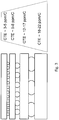
- Fig. 3 is a schematic cross-section showing different values of CTE in a stack of components (a so called "CTE pyramid for interposers")
- Fig. 4 schematically shows an example of a prior art solution to the problem of temperature matching of components with large differences in CTE.
- IC integrated circuits
- I/O interposer
- CTE a CTE of about 3 ppm/C.
- I/O interposer
- a CTE of about 3 ppm/C silicon or glass interposer IP
- a Module/Processor PCB having a high CTE of about 18-22 ppm/C.
- BGA All Grid Array
- underfill between on one hand the IC component and the interposer, and on the other between the PCB and the BGA substrate.
- This underfill is applied as a liquid that is drawn into the very small spacing by capillary force.
- An interposer according to the invention is defined in claim 1.
- the benefit of using a rigid interposer is i.a. an ability to create TSVs through full wafer thickness.
- the stress gradient across a thick interposer is reduced, and it can be directly attached to the PCB and will accommodate stresses.
- rigid interposers best take advantage of existing wafer processing, and there is no need for complex thin wafer handling.
- the inventive merit of the present interposer is that it is possible to taylor the coefficient of thermal expansion CTE of the interposer to match components to be attached thereto within very wide ranges.
- the invention eliminates organic substrates which improves heat transfer, thermal matching of die to package.
- a silicon substrate can furthermore be “functionalized” by incorporating passive (resistances, capacitances, inductances) or active elements (e.g. diodes and ESD protection), which is not possible with organic substrates.
- a further advantage is a more cost efficient structure, in that only one substrate is needed.
- a method of making an interposer comprising providing a substrate having a front side and a back side; making a double via having a narrow part and a wide part; depositing metal at least as a liner layer inside the via on its walls; providing redistribution structures in the surface(s) of the substrate which are flush with at least the front side of the substrate; making contact elements on the redistribution structures on the front side, said contact elements having an aspect ratio, height:diameter ⁇ 1:1, preferably 1:1 to 2:1.
- wafers are disclosed with hermetically sealed and close-packed vias and with in-plane routing patterns, such that the advantages of both of the above described prior art structures are combined in one structure.
- the prior art structure according to Fig. 1 comprises a conventional metal via, where the diameter is in the order of 300 ⁇ m.
- This structure is fairly easy to manufacture as long as the pitch, i.e. center-to-center distance between vias is not too small. Density of vias is of course also important.
- thermal stress effects may easily cause damage to the substrate, both during manufacture and use.
- the diameter of the via holes must be reduced.
- the aspect ratio (Depth/Width) is high, i.e. is more than 2:1, and even for aspect ratios down to 1:1 it may be difficult, due to the nature of the PVD process and step coverage.
- the seed layer on the field i.e. the flat wafer area surrounding the vias and the RDL structures
- the seed layer on the field i.e. the flat wafer area surrounding the vias and the RDL structures
- the RDL are to be made needs to be thick and therefore makes densely packed redistribution wires with small feature size difficult to obtain, when the seed layer is to be removed by wet etching processes.
- Fig. 2 is very flexible/adaptable in terms of the amount of metal that can be introduced in it.
- the top portion is filled with metal, whereas the bottom portion has only the walls thereof coated, as a "liner" of metal.
- this liner thicker or thinner, the temperature expansion properties can be varied to adapt to components to be attached to the interposer, primarily by virtue of there being air present in the via, which renders it able to accommodate movements. Instead letting air being present other materials can be provided, which is described further below.
- Interposers in general are used for connecting devices having high density I/Os with devices having low density I/Os.
- matching of devices having different CTE is made by using a so called underfill, which is a material that is applied in the very small spacing between a device having one CTE and another device having a differing CTE.
- the inventive merit of the present interposer is that it is possible to taylor the coefficient of thermal expansion CTE of the interposer to match components to be attached thereto within very wide ranges.
- the invention essentially resides in the adaption of the CTE of the interposer to the extremes in CTE represented by the silicon die on one side of the interposer and the plastic or ceramic circuit board on the other side of the interposer.
- the CTE of the interposer is thereby selected to be somewhere in between these extremes, which prevents undue strain and stress that the interposer otherwise might be subjected to.
- One way is to select the width of the via holes according to the situation, where wider vias (i.e. more metal) will increase the CTE and narrower vias will reduce the CTE.
- wider vias i.e. more metal
- narrower vias will reduce the CTE.
- the routing structures can also be made to exhibit primarily larger depth. The width would normally be required to be small because of the need to close-pack the structures.
- Another method is to provide thermal expansion matching structures, i.e. non-functional vias and/or recesses. Thereby the width and depth of the recesses and vias can be taylored to the situation at hand, and also the density of structures can be increased if required.
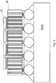
- Fig. 5 schematically illustrates the invention showing a plurality of integrated circuits IC on top of the interposer which is attached directly to a circuit board PCB.
- the interposer is one single, rigid component structure IP that replaces the multi-layered structure according to prior art ( Fig. 4 ).
- Fig. 6 illustrates an embodiment of an interposer in more detail. It comprises a substrate 10 in which double vias 18, 28 have been made.
- the double vias comprise a wide 28 and a narrow portion 18, and in the shown embodiment the narrow part is filled with metal 27 whereas the wider portion only has a "liner layer" of metal provided.
- routing 20 on the front side FS on which contact elements, suitably pillars ⁇ SB, are provided. These contact elements help in accommodating lateral movements due to thermal effects.
- On the back side BS there are further routing and contacts, e.g. Ball Grid Arrays BGA.
- the contact elements (pillars) are made of copper or at least are copper based.
- Fig. 7 illustrates an embodiment of an interposer according to the invention having the mentioned "double" vias and connecting a printed circuit board PCB with a silicon device SD on top, said device having a high density of I/O:s, i.e. very close spacing between them.
- the circuit board which can be a laminate, PCB, Ceramic etc with a low density of I/O:s, is attached.
- contact elements in the form of contact elements ⁇ SB with a very small pitch (e.g. 50 ⁇ m spacing), or regular SMD solder ⁇ -bumps.
- the contact elements will exhibit dimensions of 20-50 ⁇ m in diameter and a height of 30-100 ⁇ m. A preferred diameter would be about 40 ⁇ m and a preferred height about 60 ⁇ m, giving an aspect ratio of 1,5:1.
- underfill UF is also provided in conventional manner between the interposer and the silicon device on the top. In particular the underfill makes it possible to fine-tune the CTE matching by providing more or less underfill between the upper components.
- the copper contact elements are made by Cu plating or other techniques well known to the skilled man in semiconductor packaging art.
- thermal expansion matching structures the sole purpose of which are to provide an adapted CTE value for the interposer.
- thermal expansion matching structures Examples of such thermal expansion matching structures are shown in Fig. 8 .
- the thermal expansion matching structure is provided as a double via DDV as shown previously, but where there are no connections to components, i.e. the via has an identical constitution as the "active" double vias but is not connected to any active components, and is thus only used for the purpose of introducing more metal in the interposer.
- the thermal expansion matching structure has a relatively thin liner layer LL of metal.
- a second example is where there is only provided a thermal expansion matching structure in the form of a recess DR in the front side (top surface as seen in the figure) and filling it with metal.
- thermal expansion matching structures can be varied within wide ranges.
- This hole is a wider hole having only a liner LL on the inner walls.
- the liner layer is shown, as an example, with at thicker liner layer LL.
- the above process is usable for relatively thick substrates, i.e. exhibiting a thickness in the order of 300 ⁇ m and more, which is a rigid enough wafer to be compatible with automatic semiconductor handling without the need for stabilizing carrier solution.
- Fig. 9 illustrates a further embodiment where the interposer IP has been provided with RDL structures 20 in several layers, suitably made by a damascene process.
- the material in which the actual routings (which are metal) are made is normally an insulator such as an oxide.
- this material in itself will exhibit a different CTE compared to the silicon in the interposer, and thus also this layered structure can also be made to provide some CTE matching.
- a further possibility to "fine tune" the CTE adjustment is illustrated in Fig. 10 .
- the remaining voids can be filled with a further elastic material P having a different CTE than the metal.
- a further elastic material P having a different CTE than the metal.
- Such material can be e.g. an elastic polymer such as a siloxane based photosensitive permanent resist, obtainable e.g. from Shinetsu under the treadname SINR®, or off stoichmetric thiol-enes (OSTE), or low temperature poly-silicon.
- Poly-silicon is of course not elastic but has a suitable CTE value that yields a similar effect as the elastic polymers.
- Fig. 10a there is shown an example not falling under the claimed invention of a "double via", having a wide part and a narrow part, where there is a liner layer LLM only of metal covering the inner walls of the via, and the elastic further material P is provided so as to fill up the void.
- Fig. 10b an example according to the invention is shown.
- the upper part of the structure i.e. the narrow part of the via and, optionally if present, also the routing structure
- metal M is completely filled with metal M
- the lower, wider part only has a liner layer, and the void in the wider part is filled with the elastic further material P.
- This feature is of course applicable in all combinations of structures as described herein, although not explicitly shown.
- One further advantage of providing a further material P as shown is that contact pads can be provided on the exposed surfaces of this material, which further improves the temperature matching.
- solder balls BGA should be slightly displaced from center such they cover the material in the liner layer only to one side, see Fig. 10a arrow at D. In this way any movement due to thermal stress will be accommodated by the combination of the solder ball and the elastic further material P provided in the via.
- Figs. 10c and 10d do not fall under the claimed invention.
- a collar C around the via is provided.
- the collar C is flush with the surrounding substrate 10 surface, and the solder ball BGA is attached partly to this collar C and partly supported by the further material P in the via. Thereby a better electrical contact is ascertained.
- a collar C' is provided. However, in this case the collar is raised above the surrounding substrate surface.
- solder balls BGA are provided entirely on the substrate.
- nay movements are entirely accommodated by the solder ball, which may cause it to shear to the extent that it breaks.
Landscapes
- Internal Circuitry In Semiconductor Integrated Circuit Devices (AREA)
- Physics & Mathematics (AREA)
- Geometry (AREA)
- Shielding Devices Or Components To Electric Or Magnetic Fields (AREA)
- Cooling Or The Like Of Semiconductors Or Solid State Devices (AREA)
Claims (10)
- Halbleiter-Interposer, umfassend:ein Substrat (10) eines Halbleitermaterials mit einer ersten Seite (FS), die mit einer Leitstruktur (20) bereitgestellt wird, und einer gegenüberliegenden zweiten Seite (BS), die ebenfalls mit einer Leitstruktur (50) bereitgestellt wird; wobeider Interposer aus einem einzelnen starren Teil hergestellt ist;der Interposer mindestens eine leitende waferdurchquerende Durchkontaktierung (18, 28, 27), das Metall (27) umfasst, aufweist, wobei die Durchkontaktierung eine Doppel-Durchkontaktierung ist, das einen ersten schmalen oberen Abschnitt und einen breiteren unteren Abschnitt umfasst, wobei der obere Abschnitt mit Metall gefüllt ist, und wobei der breitere untere Abschnitt nur an seinen Wänden mit einer Oberflächenbeschichtung aus Metall beschichtet ist;der Interposer mindestens eine Aussparung (20) aufweist, die auf der ersten Seite des Substrats (10) und in dem Halbleitermaterial des Substrats bereitgestellt wird, wobei die Aussparung mit Metall gefüllt und mit der waferdurchquerenden Durchkontaktierung verbunden ist, wodurch die Leitstruktur (20) bereitgestellt wird;die freigelegten Flächen der metallgefüllten Durchkontaktierung und die metallgefüllte Aussparung (18, 27) im Wesentlichen mit der Substratoberfläche auf der ersten Seite des Substrats bündig sind;der Interposer Mikrosäulen aus Cu mit einer sehr kleinen Neigung, vorzugsweise etwa 50 µm, umfasst, die auf der Substratoberfläche auf der ersten Seite (FS) des Substrats angeordnet sind;wobei der erste schmale obere Abschnitt der Durchkontaktierung vollständig mit Metall gefüllt ist und der breitere untere Abschnitt mit einer Auskleidungsschicht aus Metall (Liner Layer of Metal; LLM) bereitgestellt wird; und dadurch, dassder Hohlraum in dem breiteren unteren Abschnitt mit einem weiteren Material (P) gefüllt ist, das aus elastischem Polymer und Poly-Silizium ausgewählt ist.
- Interposer nach Anspruch 1, wobei die Säulen vorzugsweise Lötsäulen sind.
- Interposer nach einem der vorstehenden Ansprüche, wobei die Höhe der Säulen 30-100 µm beträgt und der Durchmesser 20-50 µm beträgt.
- Interposer nach einem der vorstehenden Ansprüche, wobei Lötkugeln (BGA) an der Rückseite des Interposers bereitgestellt werden, derart leicht versetzt von der Mitte einer Durchkontaktierung, dass sie das Material in der Auskleidungsschicht nur zu einer Seite bedecken.
- Interposer nach einem der vorstehenden Ansprüche, wobei ein Kragen (C) um die Durchkontaktierung auf der Rückseite bereitgestellt wird, wobei der Kragen bündig mit der umgebenden Oberfläche des Substrats (10) ist, und wobei die Lötkugel BGA teilweise an diesem Kragen (C) befestigt ist und teilweise von dem weiteren Material P in der Durchkontaktierung gestützt wird.
- Interposer nach einem der vorstehenden Ansprüche, wobei ein Kragen (C) um die Durchkontaktierung auf der Rückseite bereitgestellt wird, wobei der Kragen über die umgebende Substratoberfläche gehoben ist.
- Halbleiterprodukt, umfassend:einen Interposer nach Anspruch 1;eine erste Struktur mit einem niedrigen Wärmeausdehnungskoeffizienten und der an der ersten Seite des Interposers befestigt ist; undeine zweite Struktur mit einem hohen Wärmeausdehnungskoeffizienten und der an der zweiten Seite des Interposers befestigt ist.
- Produkt nach Anspruch 7, wobei die erste Struktur eine integrierte Schaltung auf Siliziumbasis ist; und wobei die zweite Struktur eine Leiterplatte ist.
- Produkt nach Anspruch 7 oder 8, wobei Unterfüllung zwischen dem Interposer und der Siliziumvorrichtung auf der Oberseite bereitgestellt wird.
- Verfahren zum Herstellen eines Interposers, Bereitstellen eines Substrats mit einer Vorderseite und einer Rückseite einer mindestens einen leitenden waferdurchquerenden Durchkontaktierung, der Metall umfasst, umfassend, wobei die Durchkontaktierung einen ersten schmalen oberen Abschnitt und einen breiteren unteren Abschnitt aufweist; Ablagern von Metall, um den oberen schmalen Abschnitt zu füllen und als eine Auskleidungsschicht innerhalb der Durchkontaktierung an den Wänden des breiteren Abschnitts; Bereitstellen von Umverteilungsstrukturen in der bzw. den Fläche(n) des Substrats, die mit mindestens der Vorderseite des Substrats bündig sind; Herstellen von Kontaktelementen auf den Umverteilungsstrukturen auf der Vorderseite, wobei die Kontaktelemente ein Seitenverhältnis Höhe:Durchmesser < 1:1 aufweisen; und Ablagern eines elastischen Polymers oder Poly-Siliziums in den Hohlräumen in der Durchkontaktierung.
Applications Claiming Priority (2)
| Application Number | Priority Date | Filing Date | Title |
|---|---|---|---|
| SE1250374A SE537874C2 (sv) | 2012-04-13 | 2012-04-13 | CTE-anpassad interposer och metod att tillverka en sådan |
| PCT/SE2013/050408 WO2013154497A2 (en) | 2012-04-13 | 2013-04-15 | Cte matched interposer and method of making |
Publications (3)
| Publication Number | Publication Date |
|---|---|
| EP2837026A2 EP2837026A2 (de) | 2015-02-18 |
| EP2837026A4 EP2837026A4 (de) | 2016-01-20 |
| EP2837026B1 true EP2837026B1 (de) | 2019-07-17 |
Family
ID=49328264
Family Applications (1)
| Application Number | Title | Priority Date | Filing Date |
|---|---|---|---|
| EP13775666.4A Active EP2837026B1 (de) | 2012-04-13 | 2013-04-15 | Zwischenstück mit angepasstem wärmeausdehnungskoeffizienten und verfahren zur herstellung |
Country Status (4)
| Country | Link |
|---|---|
| US (1) | US9224681B2 (de) |
| EP (1) | EP2837026B1 (de) |
| SE (1) | SE537874C2 (de) |
| WO (1) | WO2013154497A2 (de) |
Families Citing this family (27)
| Publication number | Priority date | Publication date | Assignee | Title |
|---|---|---|---|---|
| SE538069C2 (sv) * | 2012-03-12 | 2016-02-23 | Silex Microsystems Ab | Metod att tillverka tätpackade viastrukturer med routing iplanet |
| US9041205B2 (en) * | 2013-06-28 | 2015-05-26 | Intel Corporation | Reliable microstrip routing for electronics components |
| US9154138B2 (en) | 2013-10-11 | 2015-10-06 | Palo Alto Research Center Incorporated | Stressed substrates for transient electronic systems |
| JP5846185B2 (ja) * | 2013-11-21 | 2016-01-20 | 大日本印刷株式会社 | 貫通電極基板及び貫通電極基板を用いた半導体装置 |
| US9433101B2 (en) | 2014-10-16 | 2016-08-30 | International Business Machines Corporation | Substrate via filling |
| US9780044B2 (en) * | 2015-04-23 | 2017-10-03 | Palo Alto Research Center Incorporated | Transient electronic device with ion-exchanged glass treated interposer |
| WO2017029822A1 (ja) * | 2015-08-18 | 2017-02-23 | 三菱電機株式会社 | 半導体装置 |
| US10012250B2 (en) | 2016-04-06 | 2018-07-03 | Palo Alto Research Center Incorporated | Stress-engineered frangible structures |
| US10026579B2 (en) | 2016-07-26 | 2018-07-17 | Palo Alto Research Center Incorporated | Self-limiting electrical triggering for initiating fracture of frangible glass |
| US10224297B2 (en) | 2016-07-26 | 2019-03-05 | Palo Alto Research Center Incorporated | Sensor and heater for stimulus-initiated fracture of a substrate |
| US10251270B2 (en) * | 2016-09-15 | 2019-04-02 | Innovium, Inc. | Dual-drill printed circuit board via |
| US10903173B2 (en) | 2016-10-20 | 2021-01-26 | Palo Alto Research Center Incorporated | Pre-conditioned substrate |
| CN107240579B (zh) * | 2017-05-23 | 2019-12-24 | 华进半导体封装先导技术研发中心有限公司 | 转接板的rdl封装成形方法 |
| US10626048B2 (en) | 2017-12-18 | 2020-04-21 | Palo Alto Research Center Incorporated | Dissolvable sealant for masking glass in high temperature ion exchange baths |
| US11152294B2 (en) * | 2018-04-09 | 2021-10-19 | Corning Incorporated | Hermetic metallized via with improved reliability |
| US10717669B2 (en) | 2018-05-16 | 2020-07-21 | Palo Alto Research Center Incorporated | Apparatus and method for creating crack initiation sites in a self-fracturing frangible member |
| US12200875B2 (en) | 2018-09-20 | 2025-01-14 | Industrial Technology Research Institute | Copper metallization for through-glass vias on thin glass |
| US20200105646A1 (en) * | 2018-10-01 | 2020-04-02 | Nanya Technology Corporation | Semiconductor structure having through silicon via structure and method for forming the same |
| US11107645B2 (en) | 2018-11-29 | 2021-08-31 | Palo Alto Research Center Incorporated | Functionality change based on stress-engineered components |
| US10947150B2 (en) | 2018-12-03 | 2021-03-16 | Palo Alto Research Center Incorporated | Decoy security based on stress-engineered substrates |
| KR20250083587A (ko) | 2019-02-21 | 2025-06-10 | 코닝 인코포레이티드 | 구리-금속화된 쓰루 홀을 갖는 유리 또는 유리 세라믹 물품 및 이를 제조하기 위한 공정 |
| US10969205B2 (en) | 2019-05-03 | 2021-04-06 | Palo Alto Research Center Incorporated | Electrically-activated pressure vessels for fracturing frangible structures |
| GB2587374B (en) | 2019-09-25 | 2022-08-17 | X Fab Semiconductor Foundries Gmbh | Through silicon via and redistribution layer |
| US12091310B2 (en) | 2020-05-27 | 2024-09-17 | Apogee Semiconductor, Inc. | Integrated circuit packages having stress-relieving features |
| US12013043B2 (en) | 2020-12-21 | 2024-06-18 | Xerox Corporation | Triggerable mechanisms and fragment containment arrangements for self-destructing frangible structures and sealed vessels |
| US11904986B2 (en) | 2020-12-21 | 2024-02-20 | Xerox Corporation | Mechanical triggers and triggering methods for self-destructing frangible structures and sealed vessels |
| KR102937571B1 (ko) | 2021-07-21 | 2026-03-10 | 삼성전자주식회사 | 반도체 패키지 |
Family Cites Families (14)
| Publication number | Priority date | Publication date | Assignee | Title |
|---|---|---|---|---|
| US6335491B1 (en) * | 2000-02-08 | 2002-01-01 | Lsi Logic Corporation | Interposer for semiconductor package assembly |
| JP2003258189A (ja) * | 2002-03-01 | 2003-09-12 | Toshiba Corp | 半導体装置及びその製造方法 |
| JP2006261255A (ja) * | 2005-03-16 | 2006-09-28 | Matsushita Electric Ind Co Ltd | 半導体装置 |
| US7667473B1 (en) * | 2005-09-28 | 2010-02-23 | Xilinx, Inc | Flip-chip package having thermal expansion posts |
| WO2008078899A1 (en) * | 2006-12-23 | 2008-07-03 | Lg Innotek Co., Ltd | Semiconductor package and manufacturing method thereof |
| US7841080B2 (en) * | 2007-05-30 | 2010-11-30 | Intel Corporation | Multi-chip packaging using an interposer with through-vias |
| CN101785103B (zh) | 2007-07-05 | 2011-12-28 | Aac微技术有限公司 | 低阻抗晶圆穿孔 |
| US20090243100A1 (en) | 2008-03-27 | 2009-10-01 | Jotaro Akiyama | Methods to Form a Three-Dimensionally Curved Pad in a Substrate and Integrated Circuits Incorporating such a Substrate |
| KR100990173B1 (ko) * | 2008-05-19 | 2010-10-29 | 삼성전기주식회사 | 인터포저를 구비하는 전자소자 패키지 및 그 제조방법 |
| SE534510C2 (sv) | 2008-11-19 | 2011-09-13 | Silex Microsystems Ab | Funktionell inkapsling |
| JP5584986B2 (ja) * | 2009-03-25 | 2014-09-10 | 富士通株式会社 | インターポーザ |
| SE538069C2 (sv) * | 2012-03-12 | 2016-02-23 | Silex Microsystems Ab | Metod att tillverka tätpackade viastrukturer med routing iplanet |
| SE538058C2 (sv) | 2012-03-30 | 2016-02-23 | Silex Microsystems Ab | Metod att tillhandahålla ett viahål och en routing-struktur |
| US20140035935A1 (en) * | 2012-08-03 | 2014-02-06 | Qualcomm Mems Technologies, Inc. | Passives via bar |
-
2012
- 2012-04-13 SE SE1250374A patent/SE537874C2/sv unknown
-
2013
- 2013-04-15 EP EP13775666.4A patent/EP2837026B1/de active Active
- 2013-04-15 WO PCT/SE2013/050408 patent/WO2013154497A2/en not_active Ceased
- 2013-04-15 US US14/391,855 patent/US9224681B2/en active Active
Non-Patent Citations (1)
| Title |
|---|
| None * |
Also Published As
| Publication number | Publication date |
|---|---|
| EP2837026A4 (de) | 2016-01-20 |
| US9224681B2 (en) | 2015-12-29 |
| EP2837026A2 (de) | 2015-02-18 |
| SE537874C2 (sv) | 2015-11-03 |
| US20150076677A1 (en) | 2015-03-19 |
| SE1250374A1 (sv) | 2013-10-14 |
| WO2013154497A3 (en) | 2013-12-05 |
| WO2013154497A2 (en) | 2013-10-17 |
| WO2013154497A4 (en) | 2014-01-23 |
Similar Documents
| Publication | Publication Date | Title |
|---|---|---|
| EP2837026B1 (de) | Zwischenstück mit angepasstem wärmeausdehnungskoeffizienten und verfahren zur herstellung | |
| US12381119B2 (en) | Seal for microelectronic assembly | |
| EP2978020B1 (de) | Gehäusesubstrat | |
| US8907471B2 (en) | Window interposed die packaging | |
| US8716859B2 (en) | Enhanced flip chip package | |
| US9548251B2 (en) | Semiconductor interposer having a cavity for intra-interposer die | |
| KR101731198B1 (ko) | 반도체 패키지 및 반도체 패키지를 위한 베이스를 제조하기 위한 방법 | |
| US20160189983A1 (en) | Method and structure for fan-out wafer level packaging | |
| TW201539660A (zh) | 堆疊晶粒積體電路 | |
| US11410968B2 (en) | Semiconductor device and method of forming the same | |
| US9334156B2 (en) | Chip package and method thereof | |
| US8582314B2 (en) | Interconnection structure, interposer, semiconductor package, and method of manufacturing interconnection structure | |
| CN115995455A (zh) | 基于玻璃中介层和硅桥结构的2.5d封装结构及其制作方法 | |
| US20250029911A1 (en) | Manufacturing method of semiconductor substrate | |
| US9431370B2 (en) | Compliant dielectric layer for semiconductor device | |
| KR20240145210A (ko) | 반도체 패키지 | |
| CN121816088A (zh) | 封装结构及其制造方法 |
Legal Events
| Date | Code | Title | Description |
|---|---|---|---|
| PUAI | Public reference made under article 153(3) epc to a published international application that has entered the european phase |
Free format text: ORIGINAL CODE: 0009012 |
|
| 17P | Request for examination filed |
Effective date: 20141014 |
|
| AK | Designated contracting states |
Kind code of ref document: A2 Designated state(s): AL AT BE BG CH CY CZ DE DK EE ES FI FR GB GR HR HU IE IS IT LI LT LU LV MC MK MT NL NO PL PT RO RS SE SI SK SM TR |
|
| AX | Request for extension of the european patent |
Extension state: BA ME |
|
| DAX | Request for extension of the european patent (deleted) | ||
| A4 | Supplementary search report drawn up and despatched |
Effective date: 20151223 |
|
| RIC1 | Information provided on ipc code assigned before grant |
Ipc: H01L 23/538 20060101ALI20151217BHEP Ipc: H01L 23/32 20060101AFI20151217BHEP Ipc: H01L 23/498 20060101ALI20151217BHEP Ipc: H01L 23/52 20060101ALI20151217BHEP |
|
| GRAJ | Information related to disapproval of communication of intention to grant by the applicant or resumption of examination proceedings by the epo deleted |
Free format text: ORIGINAL CODE: EPIDOSDIGR1 |
|
| STAA | Information on the status of an ep patent application or granted ep patent |
Free format text: STATUS: GRANT OF PATENT IS INTENDED |
|
| GRAP | Despatch of communication of intention to grant a patent |
Free format text: ORIGINAL CODE: EPIDOSNIGR1 |
|
| INTG | Intention to grant announced |
Effective date: 20190410 |
|
| RIN1 | Information on inventor provided before grant (corrected) |
Inventor name: EBEFORS, THORBJOERN Inventor name: PERTTU, DANIEL |
|
| GRAS | Grant fee paid |
Free format text: ORIGINAL CODE: EPIDOSNIGR3 |
|
| GRAA | (expected) grant |
Free format text: ORIGINAL CODE: 0009210 |
|
| STAA | Information on the status of an ep patent application or granted ep patent |
Free format text: STATUS: THE PATENT HAS BEEN GRANTED |
|
| AK | Designated contracting states |
Kind code of ref document: B1 Designated state(s): AL AT BE BG CH CY CZ DE DK EE ES FI FR GB GR HR HU IE IS IT LI LT LU LV MC MK MT NL NO PL PT RO RS SE SI SK SM TR |
|
| REG | Reference to a national code |
Ref country code: GB Ref legal event code: FG4D |
|
| REG | Reference to a national code |
Ref country code: CH Ref legal event code: EP |
|
| REG | Reference to a national code |
Ref country code: IE Ref legal event code: FG4D |
|
| REG | Reference to a national code |
Ref country code: DE Ref legal event code: R096 Ref document number: 602013057923 Country of ref document: DE |
|
| REG | Reference to a national code |
Ref country code: AT Ref legal event code: REF Ref document number: 1156628 Country of ref document: AT Kind code of ref document: T Effective date: 20190815 |
|
| REG | Reference to a national code |
Ref country code: NL Ref legal event code: MP Effective date: 20190717 |
|
| REG | Reference to a national code |
Ref country code: LT Ref legal event code: MG4D |
|
| REG | Reference to a national code |
Ref country code: AT Ref legal event code: MK05 Ref document number: 1156628 Country of ref document: AT Kind code of ref document: T Effective date: 20190717 |
|
| PG25 | Lapsed in a contracting state [announced via postgrant information from national office to epo] |
Ref country code: FI Free format text: LAPSE BECAUSE OF FAILURE TO SUBMIT A TRANSLATION OF THE DESCRIPTION OR TO PAY THE FEE WITHIN THE PRESCRIBED TIME-LIMIT Effective date: 20190717 Ref country code: SE Free format text: LAPSE BECAUSE OF FAILURE TO SUBMIT A TRANSLATION OF THE DESCRIPTION OR TO PAY THE FEE WITHIN THE PRESCRIBED TIME-LIMIT Effective date: 20190717 Ref country code: AT Free format text: LAPSE BECAUSE OF FAILURE TO SUBMIT A TRANSLATION OF THE DESCRIPTION OR TO PAY THE FEE WITHIN THE PRESCRIBED TIME-LIMIT Effective date: 20190717 Ref country code: LT Free format text: LAPSE BECAUSE OF FAILURE TO SUBMIT A TRANSLATION OF THE DESCRIPTION OR TO PAY THE FEE WITHIN THE PRESCRIBED TIME-LIMIT Effective date: 20190717 Ref country code: HR Free format text: LAPSE BECAUSE OF FAILURE TO SUBMIT A TRANSLATION OF THE DESCRIPTION OR TO PAY THE FEE WITHIN THE PRESCRIBED TIME-LIMIT Effective date: 20190717 Ref country code: NO Free format text: LAPSE BECAUSE OF FAILURE TO SUBMIT A TRANSLATION OF THE DESCRIPTION OR TO PAY THE FEE WITHIN THE PRESCRIBED TIME-LIMIT Effective date: 20191017 Ref country code: NL Free format text: LAPSE BECAUSE OF FAILURE TO SUBMIT A TRANSLATION OF THE DESCRIPTION OR TO PAY THE FEE WITHIN THE PRESCRIBED TIME-LIMIT Effective date: 20190717 Ref country code: PT Free format text: LAPSE BECAUSE OF FAILURE TO SUBMIT A TRANSLATION OF THE DESCRIPTION OR TO PAY THE FEE WITHIN THE PRESCRIBED TIME-LIMIT Effective date: 20191118 Ref country code: BG Free format text: LAPSE BECAUSE OF FAILURE TO SUBMIT A TRANSLATION OF THE DESCRIPTION OR TO PAY THE FEE WITHIN THE PRESCRIBED TIME-LIMIT Effective date: 20191017 |
|
| PG25 | Lapsed in a contracting state [announced via postgrant information from national office to epo] |
Ref country code: AL Free format text: LAPSE BECAUSE OF FAILURE TO SUBMIT A TRANSLATION OF THE DESCRIPTION OR TO PAY THE FEE WITHIN THE PRESCRIBED TIME-LIMIT Effective date: 20190717 Ref country code: LV Free format text: LAPSE BECAUSE OF FAILURE TO SUBMIT A TRANSLATION OF THE DESCRIPTION OR TO PAY THE FEE WITHIN THE PRESCRIBED TIME-LIMIT Effective date: 20190717 Ref country code: GR Free format text: LAPSE BECAUSE OF FAILURE TO SUBMIT A TRANSLATION OF THE DESCRIPTION OR TO PAY THE FEE WITHIN THE PRESCRIBED TIME-LIMIT Effective date: 20191018 Ref country code: RS Free format text: LAPSE BECAUSE OF FAILURE TO SUBMIT A TRANSLATION OF THE DESCRIPTION OR TO PAY THE FEE WITHIN THE PRESCRIBED TIME-LIMIT Effective date: 20190717 Ref country code: ES Free format text: LAPSE BECAUSE OF FAILURE TO SUBMIT A TRANSLATION OF THE DESCRIPTION OR TO PAY THE FEE WITHIN THE PRESCRIBED TIME-LIMIT Effective date: 20190717 Ref country code: IS Free format text: LAPSE BECAUSE OF FAILURE TO SUBMIT A TRANSLATION OF THE DESCRIPTION OR TO PAY THE FEE WITHIN THE PRESCRIBED TIME-LIMIT Effective date: 20191117 |
|
| PG25 | Lapsed in a contracting state [announced via postgrant information from national office to epo] |
Ref country code: TR Free format text: LAPSE BECAUSE OF FAILURE TO SUBMIT A TRANSLATION OF THE DESCRIPTION OR TO PAY THE FEE WITHIN THE PRESCRIBED TIME-LIMIT Effective date: 20190717 |
|
| PG25 | Lapsed in a contracting state [announced via postgrant information from national office to epo] |
Ref country code: RO Free format text: LAPSE BECAUSE OF FAILURE TO SUBMIT A TRANSLATION OF THE DESCRIPTION OR TO PAY THE FEE WITHIN THE PRESCRIBED TIME-LIMIT Effective date: 20190717 Ref country code: PL Free format text: LAPSE BECAUSE OF FAILURE TO SUBMIT A TRANSLATION OF THE DESCRIPTION OR TO PAY THE FEE WITHIN THE PRESCRIBED TIME-LIMIT Effective date: 20190717 Ref country code: EE Free format text: LAPSE BECAUSE OF FAILURE TO SUBMIT A TRANSLATION OF THE DESCRIPTION OR TO PAY THE FEE WITHIN THE PRESCRIBED TIME-LIMIT Effective date: 20190717 Ref country code: DK Free format text: LAPSE BECAUSE OF FAILURE TO SUBMIT A TRANSLATION OF THE DESCRIPTION OR TO PAY THE FEE WITHIN THE PRESCRIBED TIME-LIMIT Effective date: 20190717 Ref country code: IT Free format text: LAPSE BECAUSE OF FAILURE TO SUBMIT A TRANSLATION OF THE DESCRIPTION OR TO PAY THE FEE WITHIN THE PRESCRIBED TIME-LIMIT Effective date: 20190717 |
|
| PG25 | Lapsed in a contracting state [announced via postgrant information from national office to epo] |
Ref country code: CZ Free format text: LAPSE BECAUSE OF FAILURE TO SUBMIT A TRANSLATION OF THE DESCRIPTION OR TO PAY THE FEE WITHIN THE PRESCRIBED TIME-LIMIT Effective date: 20190717 Ref country code: IS Free format text: LAPSE BECAUSE OF FAILURE TO SUBMIT A TRANSLATION OF THE DESCRIPTION OR TO PAY THE FEE WITHIN THE PRESCRIBED TIME-LIMIT Effective date: 20200224 Ref country code: SM Free format text: LAPSE BECAUSE OF FAILURE TO SUBMIT A TRANSLATION OF THE DESCRIPTION OR TO PAY THE FEE WITHIN THE PRESCRIBED TIME-LIMIT Effective date: 20190717 Ref country code: SK Free format text: LAPSE BECAUSE OF FAILURE TO SUBMIT A TRANSLATION OF THE DESCRIPTION OR TO PAY THE FEE WITHIN THE PRESCRIBED TIME-LIMIT Effective date: 20190717 |
|
| REG | Reference to a national code |
Ref country code: DE Ref legal event code: R097 Ref document number: 602013057923 Country of ref document: DE |
|
| PLBE | No opposition filed within time limit |
Free format text: ORIGINAL CODE: 0009261 |
|
| STAA | Information on the status of an ep patent application or granted ep patent |
Free format text: STATUS: NO OPPOSITION FILED WITHIN TIME LIMIT |
|
| PG2D | Information on lapse in contracting state deleted |
Ref country code: IS |
|
| 26N | No opposition filed |
Effective date: 20200603 |
|
| PG25 | Lapsed in a contracting state [announced via postgrant information from national office to epo] |
Ref country code: SI Free format text: LAPSE BECAUSE OF FAILURE TO SUBMIT A TRANSLATION OF THE DESCRIPTION OR TO PAY THE FEE WITHIN THE PRESCRIBED TIME-LIMIT Effective date: 20190717 |
|
| PG25 | Lapsed in a contracting state [announced via postgrant information from national office to epo] |
Ref country code: MC Free format text: LAPSE BECAUSE OF FAILURE TO SUBMIT A TRANSLATION OF THE DESCRIPTION OR TO PAY THE FEE WITHIN THE PRESCRIBED TIME-LIMIT Effective date: 20190717 |
|
| REG | Reference to a national code |
Ref country code: CH Ref legal event code: PL |
|
| PG25 | Lapsed in a contracting state [announced via postgrant information from national office to epo] |
Ref country code: CH Free format text: LAPSE BECAUSE OF NON-PAYMENT OF DUE FEES Effective date: 20200430 Ref country code: LI Free format text: LAPSE BECAUSE OF NON-PAYMENT OF DUE FEES Effective date: 20200430 Ref country code: LU Free format text: LAPSE BECAUSE OF NON-PAYMENT OF DUE FEES Effective date: 20200415 |
|
| REG | Reference to a national code |
Ref country code: BE Ref legal event code: MM Effective date: 20200430 |
|
| PG25 | Lapsed in a contracting state [announced via postgrant information from national office to epo] |
Ref country code: BE Free format text: LAPSE BECAUSE OF NON-PAYMENT OF DUE FEES Effective date: 20200430 |
|
| PG25 | Lapsed in a contracting state [announced via postgrant information from national office to epo] |
Ref country code: IE Free format text: LAPSE BECAUSE OF NON-PAYMENT OF DUE FEES Effective date: 20200415 |
|
| PG25 | Lapsed in a contracting state [announced via postgrant information from national office to epo] |
Ref country code: MT Free format text: LAPSE BECAUSE OF FAILURE TO SUBMIT A TRANSLATION OF THE DESCRIPTION OR TO PAY THE FEE WITHIN THE PRESCRIBED TIME-LIMIT Effective date: 20190717 Ref country code: CY Free format text: LAPSE BECAUSE OF FAILURE TO SUBMIT A TRANSLATION OF THE DESCRIPTION OR TO PAY THE FEE WITHIN THE PRESCRIBED TIME-LIMIT Effective date: 20190717 |
|
| PG25 | Lapsed in a contracting state [announced via postgrant information from national office to epo] |
Ref country code: MK Free format text: LAPSE BECAUSE OF FAILURE TO SUBMIT A TRANSLATION OF THE DESCRIPTION OR TO PAY THE FEE WITHIN THE PRESCRIBED TIME-LIMIT Effective date: 20190717 |
|
| REG | Reference to a national code |
Ref country code: FR Ref legal event code: PLFP Year of fee payment: 11 |
|
| PGFP | Annual fee paid to national office [announced via postgrant information from national office to epo] |
Ref country code: DE Payment date: 20250423 Year of fee payment: 13 |
|
| PGFP | Annual fee paid to national office [announced via postgrant information from national office to epo] |
Ref country code: FR Payment date: 20250417 Year of fee payment: 13 |
|
| REG | Reference to a national code |
Ref country code: DE Ref legal event code: R079 Ref document number: 602013057923 Country of ref document: DE Free format text: PREVIOUS MAIN CLASS: H01L0023320000 Ipc: H10W0078000000 |
|
| PGFP | Annual fee paid to national office [announced via postgrant information from national office to epo] |
Ref country code: GB Payment date: 20260325 Year of fee payment: 14 |