EP2839501B1 - Freie schicht mit hoher thermischer stabilität für anwendungen einer magnetischen vorrichtung durch einsetzen einer bordünnschicht - Google Patents
Freie schicht mit hoher thermischer stabilität für anwendungen einer magnetischen vorrichtung durch einsetzen einer bordünnschicht Download PDFInfo
- Publication number
- EP2839501B1 EP2839501B1 EP13777528.4A EP13777528A EP2839501B1 EP 2839501 B1 EP2839501 B1 EP 2839501B1 EP 13777528 A EP13777528 A EP 13777528A EP 2839501 B1 EP2839501 B1 EP 2839501B1
- Authority
- EP
- European Patent Office
- Prior art keywords
- layer
- dusting
- free
- free layer
- layers
- Prior art date
- Legal status (The legal status is an assumption and is not a legal conclusion. Google has not performed a legal analysis and makes no representation as to the accuracy of the status listed.)
- Active
Links
Images

Classifications
-
- G—PHYSICS
- G01—MEASURING; TESTING
- G01R—MEASURING ELECTRIC VARIABLES; MEASURING MAGNETIC VARIABLES
- G01R33/00—Arrangements or instruments for measuring magnetic variables
- G01R33/02—Measuring direction or magnitude of magnetic fields or magnetic flux
- G01R33/06—Measuring direction or magnitude of magnetic fields or magnetic flux using galvano-magnetic devices
- G01R33/09—Magnetoresistive devices
- G01R33/091—Constructional adaptation of the sensor to specific applications
-
- G—PHYSICS
- G11—INFORMATION STORAGE
- G11B—INFORMATION STORAGE BASED ON RELATIVE MOVEMENT BETWEEN RECORD CARRIER AND TRANSDUCER
- G11B5/00—Recording by magnetisation or demagnetisation of a record carrier; Reproducing by magnetic means; Record carriers therefor
- G11B5/127—Structure or manufacture of heads, e.g. inductive
- G11B5/33—Structure or manufacture of flux-sensitive heads, i.e. for reproduction only; Combination of such heads with means for recording or erasing only
- G11B5/39—Structure or manufacture of flux-sensitive heads, i.e. for reproduction only; Combination of such heads with means for recording or erasing only using magneto-resistive devices or effects
- G11B5/3903—Structure or manufacture of flux-sensitive heads, i.e. for reproduction only; Combination of such heads with means for recording or erasing only using magneto-resistive devices or effects using magnetic thin film layers or their effects, the films being part of integrated structures
- G11B5/3906—Details related to the use of magnetic thin film layers or to their effects
-
- H—ELECTRICITY
- H01—ELECTRIC ELEMENTS
- H01F—MAGNETS; INDUCTANCES; TRANSFORMERS; SELECTION OF MATERIALS FOR THEIR MAGNETIC PROPERTIES
- H01F10/00—Thin magnetic films, e.g. of one-domain structure
- H01F10/32—Spin-exchange-coupled multilayers, e.g. nanostructured superlattices
- H01F10/324—Exchange coupling of magnetic film pairs via a very thin non-magnetic spacer, e.g. by exchange with conduction electrons of the spacer
- H01F10/3286—Spin-exchange coupled multilayers having at least one layer with perpendicular magnetic anisotropy
-
- H—ELECTRICITY
- H01—ELECTRIC ELEMENTS
- H01F—MAGNETS; INDUCTANCES; TRANSFORMERS; SELECTION OF MATERIALS FOR THEIR MAGNETIC PROPERTIES
- H01F10/00—Thin magnetic films, e.g. of one-domain structure
- H01F10/32—Spin-exchange-coupled multilayers, e.g. nanostructured superlattices
- H01F10/324—Exchange coupling of magnetic film pairs via a very thin non-magnetic spacer, e.g. by exchange with conduction electrons of the spacer
- H01F10/3295—Spin-exchange coupled multilayers wherein the magnetic pinned or free layers are laminated without anti-parallel coupling within the pinned and free layers
-
- H—ELECTRICITY
- H01—ELECTRIC ELEMENTS
- H01F—MAGNETS; INDUCTANCES; TRANSFORMERS; SELECTION OF MATERIALS FOR THEIR MAGNETIC PROPERTIES
- H01F41/00—Apparatus or processes specially adapted for manufacturing or assembling magnets, inductances or transformers; Apparatus or processes specially adapted for manufacturing materials characterised by their magnetic properties
- H01F41/14—Apparatus or processes specially adapted for manufacturing or assembling magnets, inductances or transformers; Apparatus or processes specially adapted for manufacturing materials characterised by their magnetic properties for applying magnetic films to substrates
- H01F41/30—Apparatus or processes specially adapted for manufacturing or assembling magnets, inductances or transformers; Apparatus or processes specially adapted for manufacturing materials characterised by their magnetic properties for applying magnetic films to substrates for applying nanostructures, e.g. by molecular beam epitaxy [MBE]
- H01F41/302—Apparatus or processes specially adapted for manufacturing or assembling magnets, inductances or transformers; Apparatus or processes specially adapted for manufacturing materials characterised by their magnetic properties for applying magnetic films to substrates for applying nanostructures, e.g. by molecular beam epitaxy [MBE] for applying spin-exchange-coupled multilayers, e.g. nanostructured superlattices
- H01F41/305—Apparatus or processes specially adapted for manufacturing or assembling magnets, inductances or transformers; Apparatus or processes specially adapted for manufacturing materials characterised by their magnetic properties for applying magnetic films to substrates for applying nanostructures, e.g. by molecular beam epitaxy [MBE] for applying spin-exchange-coupled multilayers, e.g. nanostructured superlattices applying the spacer or adjusting its interface, e.g. in order to enable particular effect different from exchange coupling
- H01F41/307—Apparatus or processes specially adapted for manufacturing or assembling magnets, inductances or transformers; Apparatus or processes specially adapted for manufacturing materials characterised by their magnetic properties for applying magnetic films to substrates for applying nanostructures, e.g. by molecular beam epitaxy [MBE] for applying spin-exchange-coupled multilayers, e.g. nanostructured superlattices applying the spacer or adjusting its interface, e.g. in order to enable particular effect different from exchange coupling insulating or semiconductive spacer
-
- H—ELECTRICITY
- H10—SEMICONDUCTOR DEVICES; ELECTRIC SOLID-STATE DEVICES NOT OTHERWISE PROVIDED FOR
- H10N—ELECTRIC SOLID-STATE DEVICES NOT OTHERWISE PROVIDED FOR
- H10N50/00—Galvanomagnetic devices
- H10N50/01—Manufacture or treatment
-
- H—ELECTRICITY
- H10—SEMICONDUCTOR DEVICES; ELECTRIC SOLID-STATE DEVICES NOT OTHERWISE PROVIDED FOR
- H10N—ELECTRIC SOLID-STATE DEVICES NOT OTHERWISE PROVIDED FOR
- H10N50/00—Galvanomagnetic devices
- H10N50/10—Magnetoresistive devices
-
- H—ELECTRICITY
- H10—SEMICONDUCTOR DEVICES; ELECTRIC SOLID-STATE DEVICES NOT OTHERWISE PROVIDED FOR
- H10N—ELECTRIC SOLID-STATE DEVICES NOT OTHERWISE PROVIDED FOR
- H10N50/00—Galvanomagnetic devices
- H10N50/80—Constructional details
- H10N50/85—Materials of the active region
-
- H—ELECTRICITY
- H01—ELECTRIC ELEMENTS
- H01F—MAGNETS; INDUCTANCES; TRANSFORMERS; SELECTION OF MATERIALS FOR THEIR MAGNETIC PROPERTIES
- H01F10/00—Thin magnetic films, e.g. of one-domain structure
- H01F10/08—Thin magnetic films, e.g. of one-domain structure characterised by magnetic layers
- H01F10/10—Thin magnetic films, e.g. of one-domain structure characterised by magnetic layers characterised by the composition
- H01F10/12—Thin magnetic films, e.g. of one-domain structure characterised by magnetic layers characterised by the composition being metals or alloys
- H01F10/123—Thin magnetic films, e.g. of one-domain structure characterised by magnetic layers characterised by the composition being metals or alloys having a L10 crystallographic structure, e.g. [Co,Fe][Pt,Pd] thin films
-
- Y—GENERAL TAGGING OF NEW TECHNOLOGICAL DEVELOPMENTS; GENERAL TAGGING OF CROSS-SECTIONAL TECHNOLOGIES SPANNING OVER SEVERAL SECTIONS OF THE IPC; TECHNICAL SUBJECTS COVERED BY FORMER USPC CROSS-REFERENCE ART COLLECTIONS [XRACs] AND DIGESTS
- Y10—TECHNICAL SUBJECTS COVERED BY FORMER USPC
- Y10T—TECHNICAL SUBJECTS COVERED BY FORMER US CLASSIFICATION
- Y10T428/00—Stock material or miscellaneous articles
- Y10T428/11—Magnetic recording head
- Y10T428/1107—Magnetoresistive
- Y10T428/1114—Magnetoresistive having tunnel junction effect
-
- Y—GENERAL TAGGING OF NEW TECHNOLOGICAL DEVELOPMENTS; GENERAL TAGGING OF CROSS-SECTIONAL TECHNOLOGIES SPANNING OVER SEVERAL SECTIONS OF THE IPC; TECHNICAL SUBJECTS COVERED BY FORMER USPC CROSS-REFERENCE ART COLLECTIONS [XRACs] AND DIGESTS
- Y10—TECHNICAL SUBJECTS COVERED BY FORMER USPC
- Y10T—TECHNICAL SUBJECTS COVERED BY FORMER US CLASSIFICATION
- Y10T428/00—Stock material or miscellaneous articles
- Y10T428/11—Magnetic recording head
- Y10T428/1107—Magnetoresistive
- Y10T428/1143—Magnetoresistive with defined structural feature
Definitions
- This disclosure relates to a magnetic devices that utilize thin films with perpendicular magnetic anisotropy (PMA) and a method for making the same, and in particular, to increasing Hc and thermal stability in the resulting multilayer magnetic stack to survive high temperature semiconductor processes up to 400°C.
- PMA perpendicular magnetic anisotropy
- Magnetoresistive Random Access Memory based on the Integration of silicon CMOS with MTJ technology, is a major emerging technology that is highly competitive with existing semiconductor memories such as SRAM, DRAM, and Flash.
- spin-transfer (spin torque or STT) magnetization switching described by C. Slonczewski in "Current driven excitation of magnetic multilayer", J. Magn. Magn. Mater. V 159, L1-L7 (1996 ), has recently stimulated considerable interest due to its potential application for spintronic devices such as STT-MRAM on a gigabit scale.
- J-G. Zhu et al. has described another spintronic device called a spin transfer oscillator (STO) in " Microwave Assisted Magnetic Recording", IEEE Trans.
- STO spin transfer oscillator
- the STO comprises a stack including a spin injection layer (SIL) with PMA character, an oscillating field generation layer (FGL) with in-plane anisotropy, and a spacer between the SIL and FGL.
- SIL spin injection layer
- FGL oscillating field generation layer
- Both MRAM and STT-MRAM may have a MTJ element based on a tunneling magneto-resistance (TMR) effect wherein a stack of layers has a configuration in which two ferromagnetic layers typically referred to as a reference layer and free layer are separated by a thin non-magnetic dielectric layer.
- the MTJ element is typically formed between a bottom electrode such as a first conductive line and a top electrode which is a second conductive line at locations where the top electrode crosses over the bottom electrode in a MRAM device.
- a MTJ element in a read head sensor may be based on a giant magnetoresistance (GMR) effect that relates to a spin valve structure where a reference layer and free layer are separated by a metal spacer.
- GMR giant magnetoresistance
- the MTJ is formed between two shields and there is a hard bias layer adjacent to the MTJ element to provide longitudinal biasing for stabilizing the free layer magnetization.
- U.S. Patent Application Publication 2005/0259365 discloses the use of a Cu or CuAg dusting layer on a top surface of a free layer in a MTJ to preserve the magnetic properties of the free layer and preserve the GMR ratio (dR/R) enhancement effects of an overlying specular scattering layer.
- a high performance MRAM MTJ element is characterized by a high tunneling magnetoresistive (TMR) ratio which is dR/R where R is the minimum resistance of the MTJ element and dR is the change in resistance observed by changing the magnetic state of the free layer.
- TMR tunneling magnetoresistive
- Rp_cov resistance uniformity
- Hc switching field
- ⁇ s magnetostriction
- the current needed to change the magnetic orientation of a magnetic region is proportional to the net polarization of the current, the volume, magnetization, Gilbert damping constant, and anisotropy field of the magnetic region to be affected.
- i c ⁇ eVMs g ⁇ H k eff , ⁇ + 1 2 H k eff , ⁇
- e the electron charge
- ⁇ a Gilbert damping constant
- Ms the saturation magnetization of the free layer
- h the reduced Plank's constant
- g the gyromagnetic ratio
- H k eff the in-plane anisotropy field
- H k eff , ⁇ the out-of-plane anisotropy field of the magnetic region to switch
- V is the volume of the free layer.
- the spin polarized current must be as small as possible.
- M s is the saturation magnetization
- d is the thickness of the magnetic element
- H k, ⁇ is the crystalline anisotropy field in the perpendicular direction
- K U ⁇ , s is the surface perpendicular anisotropy of the top and bottom surfaces of the magnetic element.
- PMA materials have magnetic anisotropy larger than that of conventional in-plane soft magnetic materials such as NiFe or CoFeB.
- magnetic devices with PMA are advantageous for achieving a low switching current and high thermal stability.
- MTJs magnetic tunnel junctions
- Eb high energy barrier
- One objective of the present disclosure is to provide a MTJ stack in a magnetic device that has a free layer with PMA and thermal stability to withstand annealing and back end of line (BEOL) processes that typically reach 400°C or higher.
- BEOL back end of line
- a second objective of the present disclosure is to provide a MTJ stack of layers according to the first objective that also has high magnetoresistance and a thermal stability factor ( ⁇ ) that are suitable for spintronic applications such as spin-torque MRAM (STT-MRAM), and microwave assisted magnetic recording (MAMR).
- STT-MRAM spin-torque MRAM
- MAMR microwave assisted magnetic recording
- MTJ magnetic tunnel junction
- Additional layers may be included such as a seed layer at the bottom of the MTJ stack that is capable of maintaining or enhancing PMA in an overlying reference layer or free layer.
- the thickness of the free layer should be less than about 20 Angstroms thick to enable perpendicular magnetic anisotropy (PMA) in the free layer.
- the reference layer also has PMA character and may be made of (Co/Ni)n laminates or the like, L1 0 ordered alloys such as FePt, CoPt. FePd, NiPt, FeNi, FeCu, MnAl, MnPt, MnPd, CuAu, or rare earth-transition metal (RE-TM) films including TbFeCo and GdFeCo.
- the tunnel barrier may be any oxide layer such as MgO, Al 2 O 3 , TiOx, or HfOx that Induces a spin dependent tunneling effect between the free layer and reference layer.
- the capping layer is a metal layer or oxide that induces or enhances out-of-plane anisotropy in the free layer in a bottom spin valve configuration.
- Each dusting layer has a thickness between 0.02 and 2.0 nm (0.2 and 20 Angstroms), and preferably between 0.02 and 1.0nm Angstroms. in a top spin valve configuration, the first dusting layer is formed between a seed layer, for example, and the free layer while the second dusting layer is between the free layer and tunnel barrier layer.
- the first dusting layer is between the tunnel barrier layer and free layer while the second dusting layer is formed between the free layer and capping layer.
- the dusting layers may be deposited at room temperature or at an elevated temperature up to 400°C. Subsequently, an anneal up to 400°C or higher, and preferably 400°C, may be employed to further improve PMA properties and thereby increase He and Hk. Furthermore, the dusting layers improve thermal stability of the free layer.
- a non-magnetic metal (M) layer may be inserted within the free layer to give a FL1/M/FL2 configuration wherein M is one of Ta, Al, Cu, Zr, Mg, Mo, or another non-magnetic metal, and FL1 and FL2 are bottom and top layers, respectively, in a composite free layer structure.
- a bottom spin valve stack preferably has a substrate/reference layer/tunnel barrier/DL1/FL1/M/FL2/ DL2/cap layer configuration where DL1 and DL2 are first and second dusting layers, respectively.
- the present disclosure is a magnetic structure with a free layer sandwiched between two boron or boron containing dusting layers to provide a combination of perpendicular magnetic anisotropy and thermal stability to at least 400°C which is suitable for applications such as MRAM and STT-MRAM, spintronic devices such as MAMR, and various designs of PMA spin valves including MTJ elements.
- the ferromagnetic layer having PMA is depicted as a free layer
- the ferromagnetic layer sandwiched between two B dusting layers may also be employed as a reference layer, pinned layer, or dipole (offset-compensation) layer as appreciated by those skilled in the art.
- dusting layers made of Co, Fe, or Ni, or alloys thereof such as NiFe, CoFe, CoTa, CoZr, CoHf, CoMg, CoNb, CoB V , or FeB V where v is from 0 to 40 atomic % were found to be effective in leading to a thermal stability of at least 400°C while maintaining substantial PMA character in magnetic tunnel junction (MTJ) structures.
- the dusting layer composition may be expanded to boron itself and alloys thereof wherein the B content is greater than 85 atomic%.
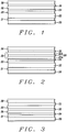
- a first embodiment of the present disclosure is depicted wherein a seed layer 21, reference layer 22 , tunnel barrier 23 , first dusting layer (DL1) 24 , free layer 25 , second dusting layer (DL2) 26 , and capping layer 30 are sequentially formed on a substrate 20 in a bottom spin valve configuration.
- All layers in the MTJ comprised of layers 21-26 and capping layer 30 may be sputter deposited in a sputter deposition mainframe that has at least one oxidation chamber and an etching chamber.
- the MTJ is part of a MRAM or STT-MRAM structure.
- reference layer 22 has PMA with a fixed magnetization in a direction perpendicular to the plane of the substrate.
- the reference layer may also have in-plane magnetization.
- the free layer 25 has PMA in a direction perpendicular to the plane of the substrate, and in the preferred embodiment is in a direction parallel or anti-parallel to that of the reference layer to give a 1 or 0 memory state.
- the substrate may be a bottom electrode in a MRAM, STT-MRAM, or spin transfer oscillator (STO), or a bottom shield in a sensor, for example.
- the reference layer 22 serves as a spin injection layer and free layer 25 functions as a field generation layer.
- Seed layer 21 is optional but is advantageously used to maintain or enhance PMA in reference layer 22 and facilitates smooth and uniform crystalline growth in the overlying MTJ layers.
- the seed layer may be a single layer or composite made of NiCr, Pd, Pt, Ta, Ru or other metals or alloys.
- Reference layer 22 may be a laminated structure such as (Co/Ni)n, (Co/Pd)n, (Co/Pt)n, or other laminated stacks exhibiting PMA where the lamination number n is between 2 and 30, and preferably from 4 to 10.
- the present disclosure also anticipates that one or more of the laminated layers may be an alloy wherein CoFe or CoFeB are employed as a replacement for Co, and NiCo, NiFe, or NiFeB are selected as a replacement for Ni.
- (Co/NiFe)n, (Co/NiFeB)n, and (Co/NiCo)n are alternatives for the reference layer.
- each Co or Co alloy layer In the laminates has a thickness between 0.05 and 0.5 nm (0.5 and 5 Angstroms) while each Pd, Pt, Ni, or Ni alloy layer has a thickness from 0.2 to 1.0 nm.
- the Co or Co alloy layer is thinner than the Ni, Ni alloy, Pt, or Pd layer.
- reference layer 22 may be comprised of an L1 0 ordered alloy such as FePt, CoPt, FePd, NiPt, FeNi, FeCu, MnAl, MnPt, MnPd, CuAu, and the like that has PMA character.
- the reference layer may be made of a RE-TM film with PMA character such as TbFeCo or GdFeCo.
- the present disclosure also encompasses an embodiment wherein the reference layer has a synthetic anti-ferromagnetic (SAF) structure with a coupling layer such as Ru formed between two reference layers RL1 and RL2 with PMA, and between two dusting layers D1 and D2 to give a RL1/D1/coupling layer/D2/RL2 configuration as previously described in related U.S. Patent 8,871,365 .
- SAF synthetic anti-ferromagnetic
- the reference layer has perpendicular magnetic anisotropy (PMA)
- a transition layer (not shown) formed between the reference layer 22 and tunnel barrier layer 23.
- the transition layer may be comprised of CoFeB, CoFe, or composites thereof, or with Co such as CoFeB/Co, and is beneficial in magnetic device designs where the reference layer Is part of a MTJ and interfaces with a tunnel barrier layer made of an oxide.
- the transition layer is formed between a reference layer with PMA and a (100) MgO tunnel barrier, for example, and is sufficiently thin to preserve the PMA property of the reference layer 22 and yet thick enough to provide a high magnetoresistance (MR) ratio.
- MR magnetoresistance
- the CoFeB portion may be from 0.4 to 0.8 nm thick, and preferably 0.6 nm, while the Co layer portion is from 0.3 to 0.5 nm (3 to 5 Angstroms), and preferably 0.4 nm thick.
- Co may be used as the upper layer in the transition layer stack and the interface with the tunnel barrier layer since it is more resistant to oxidation than a CoFeB (or CoFe) layer.
- the tunnel barrier layer 23 may be any oxide layer that Induces a spin dependent tunneling effect between the reference layer and free layer.
- MgO, Al 2 O 3 MgO, Al 2 O 3 .
- TMR tunnel magnetoresistance
- the free layer 25 has a bottom surface that contacts a first dusting layer and a top surface which contacts a second dusting layer.
- one of the two dusting layers may be omitted but it should be understood that a single dusting layer does not provide the full advantage in terms of improved thermal stability and maintaining high PMA in the free layer as achieved with two dusting layers.
- the free layer may be CoFe, Co, CoFeB, or a CoFeB alloy such as CoFeNiB, for example.
- the free layer is a single layer having a thickness from 0.5 to 2.0 nm (5 to 20 Angstroms). With thicknesses greater than about 3.0 nm, the free layer tends to have in-plane magnetization.
- interfacial perpendicular anisotropy is established between oxide and magnetic metal.
- a free layer which normally has in-plane magnetization, adjoins or is formed proximate to an oxide layer such as a MgO tunnel barrier
- the magnetization of the free layer can be aligned out-of-plane under conditions where interfacial perpendicular anisotropy exceeds the shape anisotropy field for the magnetic layer.
- the thickness of free layer 25 is represented by "d" in equation (5) presented previously.
- the shape anisotropy field for a Co 20 Fe 60 B 20 free layer is approximately 12000 Oe.
- interfacial perpendicular anisotropy may be greater than 12000 Oe by maintaining thicknesses in the 0.5 to 2.0 nm (5 to 20 Angstrom) range. Under such conditions, an out-of-plane magnetization (perpendicular anisotropy) is established in the free layer. If the free layer thickness is above about 1.9-2.0 nm (19-20 Angstroms), then the shape anisotropy field is too large to be overcome by an out-of plane component, and the magnetization of the free layer remains in-plane.
- top surface of the free layer is formed in close proximity to a capping layer made of an oxide, then interfacial perpendicular anisotropy is also established along the top surface of the free layer which further enhances PMA in free layer 25.
- a first dusting layer (DL1) 24 is formed between the tunnel barrier 23 and free layer 25 and a second dusting layer (DL2) 26 is positioned between the free layer and cap layer 30.
- DL1 and DL2 are made of B, or a B alloy such as CoB or FeB wherein the B content is >85 atomic %, and have a thickness from 0.02 to 2.0 nm (0.2 to 20 Angstroms) and preferably between 0.02 and 1.0 nm (0.2 and 10 Angstroms). Note that the DL1 composition and thickness is not necessarily equal to the DL2 composition and thickness. DL1 and DL2 thicknesses are minimized to avoid a significant reduction in the influence of the tunnel barrier layer and cap layer to induce PMA in the free layer.
- the Ku (anisotropy constant) for the free layer impacts the Eb (energy barrier) of the memory cell and it is believed that inserting dusting layers 24, 26 also increases the PMA Ku of the free layer thereby increasing Eb and enhancing the retention time of STT-MRAM designs.
- the dusting layers may be deposited at room temperature or at elevated temperatures up to 400°C and can be used as deposited or after an additional anneal at 400°C or higher, and preferably about 400°C, once all the MTJ layers are deposited.
- the present disclosure also anticipates that one or both of the DL1 and DL2 layer may be a composite comprising a plurality of boron containing dusting layers in a laminated structure.
- a moderate B concentration in the dusting layer between the tunnel barrier and free layer, and between the free layer and cap layer Is a key parameter for thermal stability enhancement.
- the thickness of a B dusting layer or the thickness and B content in a CoB or FeB dusting layer may be reduced accordingly.
- the thickness of a CoB or FeB dusting layer is also minimized to avoid adding a significant moment to the free layer magnetization which would lead to a lower PMA magnitude.
- a capping layer 30 is formed as the uppermost layer in the MTJ stack and may be comprised of one or more of Ta, Ru, Cu, Cr, or other metals that induce interfacial perpendicular anisotropy in the free layer.
- the capping layer is an oxide of a single element or an oxide of an alloy such as MgTaOx, MgZrOx, MgHfOx, MgNbOx, MgO, SiOx, SrTiOx, BaTiOx, CaTiOx, LaAlOx, MnOx, VOx, Al 2 O 3 , TiOx, BOx, and HfOx, and is preferably MgTaOx where the Mg:Ta ratio is from about 2:1 to 1:1.
- the capping layer may also be a lamination of one or more of the aforementioned oxides.
- a MgTaOx cap layer is fabricated by first sputter depositing a MgTa layer with a thickness from 0.2 to 1.0 nm (2 to 10 Angstroms), or depositing a Mg layer followed by a Ta layer to give a Mg/Ta stack. Then, either a radical (ROX) oxidation or natural (NOX) oxidation may be employed as a second step.
- ROX radical
- NOX natural
- the metal oxide cap does contribute to the overall RA value for the MTJ which means the thickness of a MgTaOx layer, for example, must be minimized to avoid a higher than desired RA.
- MgTaOx is preferred over MgO for the capping layer since the former contributes a lower RA value than an equivalent thickness of MgO.
- the free layer 25 configuration Is now FL1/M/FL2 where the metal (M) layer 28 is Ta, Al, Cu, Zr, Hf, Nb, Mg, or Mo, and the free layer is comprised of a lower FL1 layer 25a that contacts a top surface of the first dusting layer 24 and an upper FL2 layer 25b that interfaces with a bottom surface of the second dusting layer 26.
- the M layer serves as a moment dilution layer and has a thickness from 0.05 to 1.0 nm (0.5 to 10 Angstroms), and preferably between 0.1 and 0.5 nm (1 and 5 Angstroms).
- capping layer 30 is preferably comprised of a metal oxide as previously described, and more preferably is made of MgTaOx in order to enhance the interfacial perpendicular anisotropy in the FL2 layer 25b while minimizing the resistance x area (RA) value.
- RA resistance x area
- the present disclosure also encompasses an embodiment with a top spin valve design wherein the first dusting layer 24, free layer 25, second dusting layer 26, tunnel barrier 23, reference layer 22, and capping layer 30 are consecutively formed on seed layer 21.
- the free layer 25 may be a single layer made of CoFe, Co, CoFeB or a CoFeB, alloy such as CoFeNiB.
- the DL1, free layer, and DL2 layers are sequentially deposited on the seed layer prior to forming the tunnel barrier.
- One or both of the DL1 and DL2 layers may be a laminated structure with a plurality of dusting layers.
- one of the dusting layers 24, 26 may be omitted although the resulting improvement in free layer thermal stability will not be as great as when both dusting layers are present.
- a top spin valve structure further comprises a non-magnetic M layer within the free layer as described earlier.
- the first dusting layer 24, FL1 layer 25a, M layer 28, FL2 layer 25b, second dusting layer 26, tunnel barrier 23, reference layer 22, and capping layer 30 are sequentially formed on a seed layer 21.
- an annealing process may be performed that Is comprised of a temperature between 200°C and 500°C, and preferably between 300°C and 400°C for a period of 1 minute to 10 hours.
- the MTJ stack may be patterned to form a plurality of MRAM (or STT-MRAM) memory cells or STO elements by a well known photolithography and etch sequence on the substrate 20.
- the substrate is a bottom electrode
- the bottom electrode may be patterned simultaneously with the overlying multilayer stack to enable a higher density of patterned structures for advanced technology designs.
- a series of unpatterned partial MTJ stacks was fabricated and the PMA property for each was measured with a vibrating sample magnetometer (VSM) in order to demonstrate the benefits of the present disclosure.
- VSM vibrating sample magnetometer
- Each of the partial stacks has a lower MgO layer, a middle free layer, and an upper capping layer.
- the Co 20 Fe 60 B 20 free layer is 1.2 nm (12 Angstroms) thick and the capping layer is a 5 nm (50 Angstrom) thick Ta layer.
- Sample B is similar to sample A except a first boron dusting layer having a 0.05 nm (0.5 Angstrom) thickness is inserted between the MgO layer and free layer, and a second boron dusting layer also 0.5 Angstroms thick is formed between the free layer and Ta capping layer according to an embodiment of the present disclosure.
- Sample C has a MgTaOx capping layer and includes a conventional free layer with a CoFeB/Ta/CoFeB configuration wherein the CoFeB layers are 8 Angstroms thick and the Ta insertion layer is 0.15 nm (1.5 Angstroms) thick.
- Sample D is similar to sample C except first and second dusting layers each 0.05 nm (0.5 Angstroms) thick are formed between the MgO and lower CoFeB layer and between the upper CoFeB layer and capping layer, respectively, according to an embodiment of the present disclosure.
- the MgTaOx capping layer is prepared by depositing a 0.4 nm (4 Angstrom) thick Mg layer on the free layer followed by depositing a 0.3 nm (3 Angstrom) thick Ta layer on the Mg layer and then performing a natural oxidation (NOX) process. All layers were deposited at room temperature and the partial MTJ stack was annealed at 400°C for 1 hour.
- the benefits of the present disclosure are an improved PMA at process temperatures up to at least 400°C or higher for a free layer in a magnetic device with increased Ku that will increase the retention time for a memory cell. These results are achieved by forming a B or B containing dusting layer along one or both of top and bottom surfaces of a free layer. A non-magnetic moment dilution layer may be inserted within the free layer to further improve PMA.
- the MTJ stacks described herein are suitable for a variety of applications including advanced STT-MRAM devices.
- the processes and materials described herein are compatible with the design and processing requirements of magnetic devices.
Landscapes
- Engineering & Computer Science (AREA)
- Chemical & Material Sciences (AREA)
- Crystallography & Structural Chemistry (AREA)
- Power Engineering (AREA)
- Manufacturing & Machinery (AREA)
- Physics & Mathematics (AREA)
- Nanotechnology (AREA)
- Spectroscopy & Molecular Physics (AREA)
- Condensed Matter Physics & Semiconductors (AREA)
- General Physics & Mathematics (AREA)
- Hall/Mr Elements (AREA)
- Mram Or Spin Memory Techniques (AREA)
Claims (23)
- Mehrschichtstapel in einer magnetischen Vorrichtung, mit:(a) einer Bezugsschicht (22);(b) einer freien Schicht (25)
mit senkrechter magnetischer Anisotropie (PMA) und mit einer Oberfläche und einer Bodenfläche;(c) einer Tunnelbarriereschicht (23)
zwischen der Bezugsschicht und der freien Schicht; und(d) eine erste Dusting-Schicht (24) und/oder eine zweite Dusting-Schicht (26), gekennzeichnet dadurch, dass
sowohl die erste als auch die zweite Dusting-Schicht aus Bor oder einer Borlegierung mit einem B-Gehalt über ca. 85 atomare % ist, wobei die erste Dusting-Schicht die Bodenfläche der freien Schicht kontaktiert und die zweite Dusting-Schicht eine Oberfläche der freien Schicht kontaktiert. - Mehrschichtstapel nach Anspruch 1, wobei die freie Schicht eine CoFe-, Co-, CoFeB-, CoFeNiB- oder CoFeB-Legierungszusammensetzung hat und eine Stärke von etwa 0,5 bis 2,0 nm (5 bis 20 Angström).
- Mehrschichtstapel nach Anspruch 1, wobei die freie Schicht außerdem eine antimagnetische Schicht (M) (28) aus Ta, Al, Cu, Zr, Nb, Hf, Mg oder Mo umfasst, mit einer Stärke von etwa 0,005 bis 1,0 nm (0,5 bis 10 Angström), um eine FL1/M/FL2-Konfiguration zu ergeben, wobei FL1 (25a)
ein Bodenteil der freien Schicht ist, die die erste Dusting-Schicht kontaktiert, und FL2 (25b) ein oberes Teil der freien Schicht ist, die die zweite Dusting-Schicht kontaktiert. - Mehrschichtstapel nach Anspruch 1, wobei die erste Dusting-Schicht (24) und/oder die zweite Dusting-Schicht eine Zusammensetzung mit einer laminierten Borstruktur ist, die Dusting-Schichten enthält.
- Mehrschichtstapel nach Anspruch 1 mit des Weiteren einer Deckschicht als oberste Schicht in dem Mehrschichtstapel, wobei die Deckschicht eine Metallschicht oder eine Metalloxidschicht ist, die die zweite Dusting-Schicht in einer Bodenspinventil-Konfiguration kontaktiert.
- Mehrschichtstapel nach Anspruch 1, des Weiteren mit:einer Saatschicht (21) auf einem Substrat.
- Mehrschichtstapel nach Anspruch 6, des Weiteren mit einer Deckschicht (30) und mit einer Bodenspinventilstruktur, in der die Saatschicht, Bezugsschicht, Tunnelbarriere, erste Dusting-Schicht, freie Schicht, zweite Dusting-Schicht und Deckschicht sequentiell auf dem Substrat gebildet sind.
- Mehrschichtstapel nach Anspruch 7, wobei die Deckschicht eines oder mehrere der folgenden umfasst: Ta, Ru, Cu oder Cr, oder sie ist MgTaOx, MgHfOx, MgNbOx, MgZrOx, MgO, SiOx, SrTiOx, BaTiOx, CaTiOx, LaAlOx, MnOx, VOx, Al2O3, TiOx, BOx, HfOx oder eine Schicht aus einem oder mehreren der obengenannten Oxide.
- Mehrschichtstapel nach Anspruch 6, wobei die freie Schicht außerdem eine antimagnetische Schicht (M) aus Ta, Al, Cu, Zr, Hf, Nb, Mg, oder Mo umfasst und eine Stärke von etwa 0,05 bis 1,0 nm (0,5 bis 10 Angström) hat, um eine FL1/M/FL2-Konfiguration zu ergeben, wobei FL1 ein Bodenteil der freien Schicht ist, die die erste Dusting-Schicht kontaktiert, und FL2 ein oberes Teil der freien Schicht ist, die die zweite Dusting-Schicht kontaktiert.
- Mehrschichtstapel nach Anspruch 9, wobei jede FL1- und FL2-Schicht eine Stärke zwischen ca. 0.5 und 1.4 nm (5 und 14 Angström) hat.
- Mehrschichtstapel nach Anspruch 6 wobei die freie Schicht eine CoFe, Co, CoFeB, CoFeNiB oder CoFeB-Legierungszusammensetzung und eine Stärke von etwa 0,5 bis 2,0 nm (5 bis 20 Angström) hat.
- Mehrschichtstapel nach Anspruch 1, wobei die erste und die zweite Dusting-Schicht aus B, CoB oder FeB sind und jede eine Stärke von etwa 0,02 bis 2,0 nm (0,2 bis 20 Angström) hat.
- Mehrschichtstapel nach Anspruch 6, des Weiteren mit einer Deckschicht und mit einer oberen Spinventilstruktur, in der die Saatschicht, die erste Dusting-Schicht, die freie Schicht, die zweite Dusting-Schicht, Tunnelbarriereschicht, Bezugsschicht und Deckschicht sequentiell auf dem Substrat gebildet sind.
- Mehrschichtstapel nach Anspruch 1, wobei die Bezugsschicht senkrechte magnetische Anisotropie (PMA) aufweist, deren eine Magnetisierungsrichtung parallel oder antiparallel zur PMA in der freien Schicht ist, um einen Speicherzustand von entweder 1 oder 0 im magnetischen Tunnelkontakt MTJ festzulegen.
- Verfahren zum Bilden eines magnetischen Tunnelkontakts (MTJ) mit senkrechter magnetischer Anisotropie (PMA) mit:(a) Ablegen einer Saatschicht (21) auf einem Substrat (20);(b) Bildung einer Bezugsschicht (22) auf der Saatschicht;(c) Bildung einer Tunnelbarriere (23) auf der Bezugsschicht (24),(d) einer freien Schicht (25) mit PMA und einer zweiten Dusting-Schicht (24),(e) Ablegen einer Deckschicht (30) auf der zweiten Dusting-Schicht; und(f) Glühen des MTJ, gekennzeichnet dadurch, dass jede erste und zweite Dusting-Schicht aus Bor oder einer Bor enthaltenden Legierung mit einem B-Gehalt über ca. 85 atomaren % ist.
- Verfahren zum Bilden eines magnetischen Tunnelkontakts (MTJ) mit senkrechter magnetischer Anisotropie (PMA) mit:(a) Ablegen einer Saatschicht (21) auf einem Substrat (20);(b) sequentiellem Ablegen einer ersten Dusting-Schicht (24), einer freien Schicht (25) und einer zweiten Dusting-Schicht (26) auf der Saatschicht;(c) Ablegen einer Tunnelbarriereschicht (23) auf der zweiten Dusting-Schicht;(d) Bilden einer Bezugsschicht (22) auf der Tunnelbarriereschicht;(e) Bilden einer Deckschicht (30) auf der Bezugsschicht, und(f) Glühen des MTJ, gekennzeichnet dadurch, dass jede erste und zweite Dusting-Schicht aus Bor oder einer Bor enthaltenden Legierung mit einem B-Gehalt über ca. 85 atomaren % ist.
- Verfahren nach Anspruch 15 oder 16 ,wobei die freie Schicht eine CoFe, Co, CoFeB, CoFeNiB oder eine CoFeB-Legierung ist und eine Stärke von ca. 0,5 bis 2,0 (5 bis 20 Angström) hat.
- Verfahren nach Anspruch 15 oder 16, wobei die freie Schicht außerdem eine antimagnetische (M) Schicht (28) umfasst, die eine der folgenden ist: Ta, Al, Cu, Zr, Hf, Nb, Mg oder Mo, um eine FL1/M/FL2-Konfiguration zu ergeben, wobei die FL1-Schicht (25a) die erste Dusting-Schicht kontaktiert und die FL2-Schicht (25b) die zweite Dusting-Schicht kontaktiert.
- Verfahren nach Anspruch 18, wobei die M-Schicht eine Stärke zwischen etwa 0.05 und 1.0 nm (0.5 und 10 Angström) hat und jede der FL1- und FL2-Schichten eine Stärke zwischen ca. 0.5 und 1.4 nm (5 und 14 Angström) hat.
- Verfahren nach Anspruch 19, wobei die Deckschicht MgTaOx ist und ein Mg:Ta Verhältnis von etwa 2:1 bis 1:1 hat, wobei die MgTaOx-Schicht durch eine Radikaloxidation gebildet wird oder ein natürliches Oxidationsverfahren aus einer MgTa-Schicht oder einem Stapel von Mg/Ta-Schichten.
- Verfahren nach Anspruch 15 oder 16, wobei die erste und die zweite Dusting-Schicht B, CoB oder FeB sind und jede eine Stärke von ca. 0,02 bis 2,0 nm (0,2 bis 20 Angström) hat.
- Verfahren nach Anspruch 17 wobei die Deckschicht eine oder mehrere der folgenden ist:Ta, Ru, Cu und Cr.
- Verfahren nach Anspruch 15 oder 16, wobei die erste und die zweite Dusting-Schicht bei einer Temperatur von Raumtemperatur aufwärts bis 400°C oder höher abgelegt werden.
Applications Claiming Priority (2)
| Application Number | Priority Date | Filing Date | Title |
|---|---|---|---|
| US13/448,557 US8852760B2 (en) | 2012-04-17 | 2012-04-17 | Free layer with high thermal stability for magnetic device applications by insertion of a boron dusting layer |
| PCT/US2013/036851 WO2013158690A1 (en) | 2012-04-17 | 2013-04-17 | Free layer with high thermal stability for magnetic device applications by insertion of a boron dusting layer |
Publications (3)
| Publication Number | Publication Date |
|---|---|
| EP2839501A1 EP2839501A1 (de) | 2015-02-25 |
| EP2839501A4 EP2839501A4 (de) | 2015-11-25 |
| EP2839501B1 true EP2839501B1 (de) | 2016-12-21 |
Family
ID=49324265
Family Applications (1)
| Application Number | Title | Priority Date | Filing Date |
|---|---|---|---|
| EP13777528.4A Active EP2839501B1 (de) | 2012-04-17 | 2013-04-17 | Freie schicht mit hoher thermischer stabilität für anwendungen einer magnetischen vorrichtung durch einsetzen einer bordünnschicht |
Country Status (3)
| Country | Link |
|---|---|
| US (1) | US8852760B2 (de) |
| EP (1) | EP2839501B1 (de) |
| WO (1) | WO2013158690A1 (de) |
Families Citing this family (100)
| Publication number | Priority date | Publication date | Assignee | Title |
|---|---|---|---|---|
| US8871365B2 (en) * | 2012-02-28 | 2014-10-28 | Headway Technologies, Inc. | High thermal stability reference structure with out-of-plane aniotropy to magnetic device applications |
| JP6251130B2 (ja) * | 2013-06-17 | 2017-12-20 | アイメックImec | 磁気メモリ素子 |
| US9490000B2 (en) * | 2014-04-10 | 2016-11-08 | Samsung Electronics Co., Ltd. | Method and system for providing thermally assisted magnetic junctions having a multi-phase operation |
| US20150303373A1 (en) * | 2014-04-17 | 2015-10-22 | Qualcomm Incorporated | Spin-transfer switching magnetic element formed from ferrimagnetic rare-earth-transition-metal (re-tm) alloys |
| US9385309B2 (en) * | 2014-04-28 | 2016-07-05 | Qualcomm Incorporated | Smooth seed layers with uniform crystalline texture for high perpendicular magnetic anisotropy materials |
| US9412401B2 (en) | 2014-05-13 | 2016-08-09 | Seagate Technology Llc | Data reader magnetic shield with CoFeNiB material |
| US9508924B2 (en) | 2014-07-03 | 2016-11-29 | Samsung Electronics Co., Ltd. | Method and system for providing rare earth magnetic junctions usable in spin transfer torque magnetic random access memory applications |
| US9230571B1 (en) * | 2014-08-26 | 2016-01-05 | Headway Technologies, Inc. | MgO based perpendicular spin polarizer in microwave assisted magnetic recording (MAMR) applications |
| KR102245748B1 (ko) | 2014-09-12 | 2021-04-29 | 삼성전자주식회사 | 자기 기억 소자 및 이의 제조 방법 |
| US9337415B1 (en) | 2015-03-20 | 2016-05-10 | HGST Netherlands B.V. | Perpendicular spin transfer torque (STT) memory cell with double MgO interface and CoFeB layer for enhancement of perpendicular magnetic anisotropy |
| US9728712B2 (en) | 2015-04-21 | 2017-08-08 | Spin Transfer Technologies, Inc. | Spin transfer torque structure for MRAM devices having a spin current injection capping layer |
| US10468590B2 (en) | 2015-04-21 | 2019-11-05 | Spin Memory, Inc. | High annealing temperature perpendicular magnetic anisotropy structure for magnetic random access memory |
| US9853206B2 (en) | 2015-06-16 | 2017-12-26 | Spin Transfer Technologies, Inc. | Precessional spin current structure for MRAM |
| US9537090B1 (en) * | 2015-06-25 | 2017-01-03 | International Business Machines Corporation | Perpendicular magnetic anisotropy free layers with iron insertion and oxide interfaces for spin transfer torque magnetic random access memory |
| US9842988B2 (en) * | 2015-07-20 | 2017-12-12 | Headway Technologies, Inc. | Magnetic tunnel junction with low defect rate after high temperature anneal for magnetic device applications |
| US9773974B2 (en) | 2015-07-30 | 2017-09-26 | Spin Transfer Technologies, Inc. | Polishing stop layer(s) for processing arrays of semiconductor elements |
| US10163479B2 (en) | 2015-08-14 | 2018-12-25 | Spin Transfer Technologies, Inc. | Method and apparatus for bipolar memory write-verify |
| KR102465539B1 (ko) | 2015-09-18 | 2022-11-11 | 삼성전자주식회사 | 자기 터널 접합 구조체를 포함하는 반도체 소자 및 그의 형성 방법 |
| US10483320B2 (en) | 2015-12-10 | 2019-11-19 | Everspin Technologies, Inc. | Magnetoresistive stack with seed region and method of manufacturing the same |
| EP4514109A3 (de) | 2015-12-10 | 2025-04-30 | Everspin Technologies, Inc. | Magnetoresistiver stapel, seed-region dafür und verfahren zur herstellung davon |
| US9741926B1 (en) * | 2016-01-28 | 2017-08-22 | Spin Transfer Technologies, Inc. | Memory cell having magnetic tunnel junction and thermal stability enhancement layer |
| US10361361B2 (en) * | 2016-04-08 | 2019-07-23 | International Business Machines Corporation | Thin reference layer for STT MRAM |
| US10475564B2 (en) * | 2016-06-29 | 2019-11-12 | Taiwan Semiconductor Manufacturing Company, Ltd. | Perpendicularly magnetized ferromagnetic layers having an oxide interface allowing for improved control of oxidation |
| KR102611463B1 (ko) | 2016-08-02 | 2023-12-08 | 삼성전자주식회사 | 자기 기억 소자 및 그 제조방법 |
| KR102566954B1 (ko) | 2016-08-04 | 2023-08-16 | 삼성전자주식회사 | 자기 메모리 소자 및 그 제조 방법 |
| US10460781B2 (en) | 2016-09-27 | 2019-10-29 | Spin Memory, Inc. | Memory device with a dual Y-multiplexer structure for performing two simultaneous operations on the same row of a memory bank |
| US10366774B2 (en) | 2016-09-27 | 2019-07-30 | Spin Memory, Inc. | Device with dynamic redundancy registers |
| US10360964B2 (en) | 2016-09-27 | 2019-07-23 | Spin Memory, Inc. | Method of writing contents in memory during a power up sequence using a dynamic redundancy register in a memory device |
| US10991410B2 (en) | 2016-09-27 | 2021-04-27 | Spin Memory, Inc. | Bi-polar write scheme |
| US10437723B2 (en) | 2016-09-27 | 2019-10-08 | Spin Memory, Inc. | Method of flushing the contents of a dynamic redundancy register to a secure storage area during a power down in a memory device |
| US10546625B2 (en) | 2016-09-27 | 2020-01-28 | Spin Memory, Inc. | Method of optimizing write voltage based on error buffer occupancy |
| US10437491B2 (en) | 2016-09-27 | 2019-10-08 | Spin Memory, Inc. | Method of processing incomplete memory operations in a memory device during a power up sequence and a power down sequence using a dynamic redundancy register |
| US10446210B2 (en) | 2016-09-27 | 2019-10-15 | Spin Memory, Inc. | Memory instruction pipeline with a pre-read stage for a write operation for reducing power consumption in a memory device that uses dynamic redundancy registers |
| US10818331B2 (en) | 2016-09-27 | 2020-10-27 | Spin Memory, Inc. | Multi-chip module for MRAM devices with levels of dynamic redundancy registers |
| CN110192288B (zh) | 2016-12-28 | 2023-04-25 | 英特尔公司 | 垂直自旋转移矩磁机构 |
| US10665777B2 (en) | 2017-02-28 | 2020-05-26 | Spin Memory, Inc. | Precessional spin current structure with non-magnetic insertion layer for MRAM |
| US10672976B2 (en) | 2017-02-28 | 2020-06-02 | Spin Memory, Inc. | Precessional spin current structure with high in-plane magnetization for MRAM |
| US9966529B1 (en) | 2017-03-17 | 2018-05-08 | Headway Technologies, Inc. | MgO insertion into free layer for magnetic memory applications |
| US10332576B2 (en) * | 2017-06-07 | 2019-06-25 | International Business Machines Corporation | Magnetic exchange coupled MTJ free layer with double tunnel barriers having low switching current and high data retention |
| US10510390B2 (en) * | 2017-06-07 | 2019-12-17 | International Business Machines Corporation | Magnetic exchange coupled MTJ free layer having low switching current and high data retention |
| US10032978B1 (en) | 2017-06-27 | 2018-07-24 | Spin Transfer Technologies, Inc. | MRAM with reduced stray magnetic fields |
| US10553642B2 (en) | 2017-08-28 | 2020-02-04 | Samsung Electronics Co., Ltd. | Method and system for providing magnetic junctions utilizing metal oxide layer(s) |
| US10529439B2 (en) | 2017-10-24 | 2020-01-07 | Spin Memory, Inc. | On-the-fly bit failure detection and bit redundancy remapping techniques to correct for fixed bit defects |
| US10481976B2 (en) | 2017-10-24 | 2019-11-19 | Spin Memory, Inc. | Forcing bits as bad to widen the window between the distributions of acceptable high and low resistive bits thereby lowering the margin and increasing the speed of the sense amplifiers |
| US10489245B2 (en) | 2017-10-24 | 2019-11-26 | Spin Memory, Inc. | Forcing stuck bits, waterfall bits, shunt bits and low TMR bits to short during testing and using on-the-fly bit failure detection and bit redundancy remapping techniques to correct them |
| US10656994B2 (en) | 2017-10-24 | 2020-05-19 | Spin Memory, Inc. | Over-voltage write operation of tunnel magnet-resistance (“TMR”) memory device and correcting failure bits therefrom by using on-the-fly bit failure detection and bit redundancy remapping techniques |
| US10395711B2 (en) | 2017-12-28 | 2019-08-27 | Spin Memory, Inc. | Perpendicular source and bit lines for an MRAM array |
| US10424726B2 (en) | 2017-12-28 | 2019-09-24 | Spin Memory, Inc. | Process for improving photoresist pillar adhesion during MRAM fabrication |
| US10891997B2 (en) | 2017-12-28 | 2021-01-12 | Spin Memory, Inc. | Memory array with horizontal source line and a virtual source line |
| US10360962B1 (en) | 2017-12-28 | 2019-07-23 | Spin Memory, Inc. | Memory array with individually trimmable sense amplifiers |
| US10395712B2 (en) | 2017-12-28 | 2019-08-27 | Spin Memory, Inc. | Memory array with horizontal source line and sacrificial bitline per virtual source |
| US10811594B2 (en) | 2017-12-28 | 2020-10-20 | Spin Memory, Inc. | Process for hard mask development for MRAM pillar formation using photolithography |
| US10840439B2 (en) | 2017-12-29 | 2020-11-17 | Spin Memory, Inc. | Magnetic tunnel junction (MTJ) fabrication methods and systems |
| US10784439B2 (en) | 2017-12-29 | 2020-09-22 | Spin Memory, Inc. | Precessional spin current magnetic tunnel junction devices and methods of manufacture |
| US10236048B1 (en) | 2017-12-29 | 2019-03-19 | Spin Memory, Inc. | AC current write-assist in orthogonal STT-MRAM |
| US10199083B1 (en) | 2017-12-29 | 2019-02-05 | Spin Transfer Technologies, Inc. | Three-terminal MRAM with ac write-assist for low read disturb |
| US10360961B1 (en) | 2017-12-29 | 2019-07-23 | Spin Memory, Inc. | AC current pre-charge write-assist in orthogonal STT-MRAM |
| US10367139B2 (en) | 2017-12-29 | 2019-07-30 | Spin Memory, Inc. | Methods of manufacturing magnetic tunnel junction devices |
| US10236047B1 (en) | 2017-12-29 | 2019-03-19 | Spin Memory, Inc. | Shared oscillator (STNO) for MRAM array write-assist in orthogonal STT-MRAM |
| US10886330B2 (en) | 2017-12-29 | 2021-01-05 | Spin Memory, Inc. | Memory device having overlapping magnetic tunnel junctions in compliance with a reference pitch |
| US10270027B1 (en) | 2017-12-29 | 2019-04-23 | Spin Memory, Inc. | Self-generating AC current assist in orthogonal STT-MRAM |
| US10424723B2 (en) | 2017-12-29 | 2019-09-24 | Spin Memory, Inc. | Magnetic tunnel junction devices including an optimization layer |
| US10546624B2 (en) | 2017-12-29 | 2020-01-28 | Spin Memory, Inc. | Multi-port random access memory |
| US10840436B2 (en) | 2017-12-29 | 2020-11-17 | Spin Memory, Inc. | Perpendicular magnetic anisotropy interface tunnel junction devices and methods of manufacture |
| US10229724B1 (en) | 2017-12-30 | 2019-03-12 | Spin Memory, Inc. | Microwave write-assist in series-interconnected orthogonal STT-MRAM devices |
| US10339993B1 (en) | 2017-12-30 | 2019-07-02 | Spin Memory, Inc. | Perpendicular magnetic tunnel junction device with skyrmionic assist layers for free layer switching |
| US10255962B1 (en) | 2017-12-30 | 2019-04-09 | Spin Memory, Inc. | Microwave write-assist in orthogonal STT-MRAM |
| US10236439B1 (en) | 2017-12-30 | 2019-03-19 | Spin Memory, Inc. | Switching and stability control for perpendicular magnetic tunnel junction device |
| US10141499B1 (en) | 2017-12-30 | 2018-11-27 | Spin Transfer Technologies, Inc. | Perpendicular magnetic tunnel junction device with offset precessional spin current layer |
| US10319900B1 (en) | 2017-12-30 | 2019-06-11 | Spin Memory, Inc. | Perpendicular magnetic tunnel junction device with precessional spin current layer having a modulated moment density |
| US10468588B2 (en) | 2018-01-05 | 2019-11-05 | Spin Memory, Inc. | Perpendicular magnetic tunnel junction device with skyrmionic enhancement layers for the precessional spin current magnetic layer |
| US10438995B2 (en) | 2018-01-08 | 2019-10-08 | Spin Memory, Inc. | Devices including magnetic tunnel junctions integrated with selectors |
| US10438996B2 (en) | 2018-01-08 | 2019-10-08 | Spin Memory, Inc. | Methods of fabricating magnetic tunnel junctions integrated with selectors |
| US10340446B1 (en) | 2018-03-06 | 2019-07-02 | International Business Machines Corporation | Semiconductor structure multilayers having a dusting material at an interface between a non-magnetic layer and a magnetic layer |
| US10446744B2 (en) | 2018-03-08 | 2019-10-15 | Spin Memory, Inc. | Magnetic tunnel junction wafer adaptor used in magnetic annealing furnace and method of using the same |
| US11107978B2 (en) | 2018-03-23 | 2021-08-31 | Spin Memory, Inc. | Methods of manufacturing three-dimensional arrays with MTJ devices including a free magnetic trench layer and a planar reference magnetic layer |
| US10734573B2 (en) | 2018-03-23 | 2020-08-04 | Spin Memory, Inc. | Three-dimensional arrays with magnetic tunnel junction devices including an annular discontinued free magnetic layer and a planar reference magnetic layer |
| US11107974B2 (en) | 2018-03-23 | 2021-08-31 | Spin Memory, Inc. | Magnetic tunnel junction devices including a free magnetic trench layer and a planar reference magnetic layer |
| US10784437B2 (en) | 2018-03-23 | 2020-09-22 | Spin Memory, Inc. | Three-dimensional arrays with MTJ devices including a free magnetic trench layer and a planar reference magnetic layer |
| US10411185B1 (en) | 2018-05-30 | 2019-09-10 | Spin Memory, Inc. | Process for creating a high density magnetic tunnel junction array test platform |
| US20200006629A1 (en) * | 2018-06-29 | 2020-01-02 | Everspin Technologies, Inc. | Systems and methods for mitigating encroachment in magnetoresistive devices |
| US10593396B2 (en) | 2018-07-06 | 2020-03-17 | Spin Memory, Inc. | Multi-bit cell read-out techniques for MRAM cells with mixed pinned magnetization orientations |
| US10692569B2 (en) | 2018-07-06 | 2020-06-23 | Spin Memory, Inc. | Read-out techniques for multi-bit cells |
| US10559338B2 (en) | 2018-07-06 | 2020-02-11 | Spin Memory, Inc. | Multi-bit cell read-out techniques |
| US10600478B2 (en) | 2018-07-06 | 2020-03-24 | Spin Memory, Inc. | Multi-bit cell read-out techniques for MRAM cells with mixed pinned magnetization orientations |
| US10686123B2 (en) | 2018-08-16 | 2020-06-16 | International Business Machines Corporation | Multilayered magnetic free layer structure for spin-transfer torque (STT) MRAM |
| US10650875B2 (en) | 2018-08-21 | 2020-05-12 | Spin Memory, Inc. | System for a wide temperature range nonvolatile memory |
| US10699761B2 (en) | 2018-09-18 | 2020-06-30 | Spin Memory, Inc. | Word line decoder memory architecture |
| US11621293B2 (en) | 2018-10-01 | 2023-04-04 | Integrated Silicon Solution, (Cayman) Inc. | Multi terminal device stack systems and methods |
| US10971680B2 (en) | 2018-10-01 | 2021-04-06 | Spin Memory, Inc. | Multi terminal device stack formation methods |
| US11009570B2 (en) | 2018-11-16 | 2021-05-18 | Samsung Electronics Co., Ltd. | Hybrid oxide/metal cap layer for boron-free free layer |
| US10580827B1 (en) | 2018-11-16 | 2020-03-03 | Spin Memory, Inc. | Adjustable stabilizer/polarizer method for MRAM with enhanced stability and efficient switching |
| WO2020106552A1 (en) * | 2018-11-19 | 2020-05-28 | Everspin Technologies, Inc. | Magnetoresistive stack with seed region and method of manufacturing the same |
| US11107979B2 (en) | 2018-12-28 | 2021-08-31 | Spin Memory, Inc. | Patterned silicide structures and methods of manufacture |
| US11404193B2 (en) | 2019-11-22 | 2022-08-02 | Western Digital Technologies, Inc. | Magnetoresistive memory device including a magnesium containing dust layer |
| US11404632B2 (en) | 2019-11-22 | 2022-08-02 | Western Digital Technologies, Inc. | Magnetoresistive memory device including a magnesium containing dust layer |
| US10950260B1 (en) | 2020-04-17 | 2021-03-16 | Western Digital Technologies, Inc. | Magnetoresistive sensor with improved magnetic properties and magnetostriction control |
| CN112509805B (zh) * | 2020-10-19 | 2022-05-27 | 山东麦格智芯机电科技有限公司 | 一种优化钴基磁性薄膜电感材料磁性能的方法 |
| KR102947801B1 (ko) | 2021-12-13 | 2026-04-03 | 삼성전자주식회사 | 자기 저항 메모리 소자 |
| US12320870B2 (en) * | 2022-07-19 | 2025-06-03 | Allegro Microsystems, Llc | Controlling out-of-plane anisotropy in an MR sensor with free layer dusting |
Family Cites Families (24)
| Publication number | Priority date | Publication date | Assignee | Title |
|---|---|---|---|---|
| US6905780B2 (en) * | 2001-02-01 | 2005-06-14 | Kabushiki Kaisha Toshiba | Current-perpendicular-to-plane-type magnetoresistive device, and magnetic head and magnetic recording-reproducing apparatus using the same |
| US20050259365A1 (en) * | 2002-03-08 | 2005-11-24 | Seagate Technology Llc | Magnetoresistive sensor with a specular scattering layer formed by deposition from an oxide target |
| US6909630B2 (en) | 2002-12-09 | 2005-06-21 | Applied Spintronics Technology, Inc. | MRAM memories utilizing magnetic write lines |
| US7002194B2 (en) | 2003-07-18 | 2006-02-21 | International Business Machines Corporation | Via AP switching |
| US20050110004A1 (en) | 2003-11-24 | 2005-05-26 | International Business Machines Corporation | Magnetic tunnel junction with improved tunneling magneto-resistance |
| US7256971B2 (en) | 2004-03-09 | 2007-08-14 | Headway Technologies, Inc. | Process and structure to fabricate CPP spin valve heads for ultra-high recording density |
| US20060042929A1 (en) | 2004-08-26 | 2006-03-02 | Daniele Mauri | Method for reactive sputter deposition of an ultra-thin metal oxide film |
| US7791845B2 (en) | 2006-12-26 | 2010-09-07 | Hitachi Global Storage Technologies Netherlands B.V. | Tunneling magnetoresistive sensor having a high iron concentration free layer and an oxides of magnesium barrier layer |
| JP4682998B2 (ja) * | 2007-03-15 | 2011-05-11 | ソニー株式会社 | 記憶素子及びメモリ |
| JP2008252008A (ja) * | 2007-03-30 | 2008-10-16 | Toshiba Corp | 磁気抵抗効果素子、およびその製造方法 |
| US8216703B2 (en) | 2008-02-21 | 2012-07-10 | Everspin Technologies, Inc. | Magnetic tunnel junction device |
| US8039913B2 (en) | 2008-10-09 | 2011-10-18 | Seagate Technology Llc | Magnetic stack with laminated layer |
| US9165625B2 (en) | 2008-10-30 | 2015-10-20 | Seagate Technology Llc | ST-RAM cells with perpendicular anisotropy |
| US8059374B2 (en) * | 2009-01-14 | 2011-11-15 | Headway Technologies, Inc. | TMR device with novel free layer structure |
| US8072800B2 (en) * | 2009-09-15 | 2011-12-06 | Grandis Inc. | Magnetic element having perpendicular anisotropy with enhanced efficiency |
| JP2012059808A (ja) * | 2010-09-07 | 2012-03-22 | Sony Corp | 記憶素子、メモリ装置 |
| JP2012160681A (ja) * | 2011-02-03 | 2012-08-23 | Sony Corp | 記憶素子、メモリ装置 |
| US9006704B2 (en) * | 2011-02-11 | 2015-04-14 | Headway Technologies, Inc. | Magnetic element with improved out-of-plane anisotropy for spintronic applications |
| US8492859B2 (en) * | 2011-02-15 | 2013-07-23 | International Business Machines Corporation | Magnetic tunnel junction with spacer layer for spin torque switched MRAM |
| US8592927B2 (en) * | 2011-05-04 | 2013-11-26 | Magic Technologies, Inc. | Multilayers having reduced perpendicular demagnetizing field using moment dilution for spintronic applications |
| US8823118B2 (en) * | 2012-01-05 | 2014-09-02 | Headway Technologies, Inc. | Spin torque transfer magnetic tunnel junction fabricated with a composite tunneling barrier layer |
| US8871365B2 (en) * | 2012-02-28 | 2014-10-28 | Headway Technologies, Inc. | High thermal stability reference structure with out-of-plane aniotropy to magnetic device applications |
| US8710603B2 (en) * | 2012-02-29 | 2014-04-29 | Headway Technologies, Inc. | Engineered magnetic layer with improved perpendicular anisotropy using glassing agents for spintronic applications |
| US8946834B2 (en) * | 2012-03-01 | 2015-02-03 | Headway Technologies, Inc. | High thermal stability free layer with high out-of-plane anisotropy for magnetic device applications |
-
2012
- 2012-04-17 US US13/448,557 patent/US8852760B2/en active Active
-
2013
- 2013-04-17 WO PCT/US2013/036851 patent/WO2013158690A1/en not_active Ceased
- 2013-04-17 EP EP13777528.4A patent/EP2839501B1/de active Active
Also Published As
| Publication number | Publication date |
|---|---|
| EP2839501A4 (de) | 2015-11-25 |
| WO2013158690A1 (en) | 2013-10-24 |
| US20130270523A1 (en) | 2013-10-17 |
| EP2839501A1 (de) | 2015-02-25 |
| US8852760B2 (en) | 2014-10-07 |
Similar Documents
| Publication | Publication Date | Title |
|---|---|---|
| US8852760B2 (en) | Free layer with high thermal stability for magnetic device applications by insertion of a boron dusting layer | |
| EP2820649B1 (de) | Freie schicht mit hoher wärmestabilität und hoher dreidimensionaler anisotropie für anwendungen mit einer magnetvorrichtung | |
| US11930717B2 (en) | Minimal thickness synthetic antiferromagnetic (SAF) structure with perpendicular magnetic anisotropy for STT-MRAM | |
| US12414476B2 (en) | Method for forming a perpendicular spin torque oscillator (PSTO) including forming a magneto resistive sensor (MR) over a spin torque oscillator (STO) | |
| US11672182B2 (en) | Seed layer for multilayer magnetic materials | |
| US9472752B2 (en) | High thermal stability reference structure with out-of-plane anisotropy for magnetic device applications | |
| EP2926349B1 (de) | Freie schicht mit anisotropie ausserhalb der ebene zu verwenden in magnetischen bauteilen | |
| US9006704B2 (en) | Magnetic element with improved out-of-plane anisotropy for spintronic applications | |
| US8274811B2 (en) | Assisting FGL oscillations with perpendicular anisotropy for MAMR | |
| US20120280336A1 (en) | Multilayers having reduced perpendicular demagnetizing field using moment dilution for spintronic applications | |
| US20120261777A1 (en) | Magnetoresistive Element and Method of Manufacturing the Same | |
| EP3264481B1 (de) | Senkrecht magnetisierte ferromagnetische schichten mit oxydschnittstelle zur ermöglichung von verbesserter oxidationssteuerung |
Legal Events
| Date | Code | Title | Description |
|---|---|---|---|
| PUAI | Public reference made under article 153(3) epc to a published international application that has entered the european phase |
Free format text: ORIGINAL CODE: 0009012 |
|
| 17P | Request for examination filed |
Effective date: 20141113 |
|
| AK | Designated contracting states |
Kind code of ref document: A1 Designated state(s): AL AT BE BG CH CY CZ DE DK EE ES FI FR GB GR HR HU IE IS IT LI LT LU LV MC MK MT NL NO PL PT RO RS SE SI SK SM TR |
|
| AX | Request for extension of the european patent |
Extension state: BA ME |
|
| DAX | Request for extension of the european patent (deleted) | ||
| RA4 | Supplementary search report drawn up and despatched (corrected) |
Effective date: 20151028 |
|
| RIC1 | Information provided on ipc code assigned before grant |
Ipc: H01L 43/12 20060101ALI20151022BHEP Ipc: H01F 10/32 20060101ALI20151022BHEP Ipc: H01L 43/10 20060101ALI20151022BHEP Ipc: H01L 43/08 20060101AFI20151022BHEP |
|
| REG | Reference to a national code |
Ref country code: DE Ref legal event code: R079 Ref document number: 602013015668 Country of ref document: DE Free format text: PREVIOUS MAIN CLASS: H01L0021000000 Ipc: H01L0043080000 |
|
| GRAP | Despatch of communication of intention to grant a patent |
Free format text: ORIGINAL CODE: EPIDOSNIGR1 |
|
| RIC1 | Information provided on ipc code assigned before grant |
Ipc: H01L 43/10 20060101ALI20160602BHEP Ipc: H01F 41/30 20060101ALI20160602BHEP Ipc: H01L 43/08 20060101AFI20160602BHEP Ipc: H01L 43/12 20060101ALI20160602BHEP Ipc: H01F 10/32 20060101ALI20160602BHEP |
|
| INTG | Intention to grant announced |
Effective date: 20160628 |
|
| GRAS | Grant fee paid |
Free format text: ORIGINAL CODE: EPIDOSNIGR3 |
|
| GRAA | (expected) grant |
Free format text: ORIGINAL CODE: 0009210 |
|
| AK | Designated contracting states |
Kind code of ref document: B1 Designated state(s): AL AT BE BG CH CY CZ DE DK EE ES FI FR GB GR HR HU IE IS IT LI LT LU LV MC MK MT NL NO PL PT RO RS SE SI SK SM TR |
|
| REG | Reference to a national code |
Ref country code: GB Ref legal event code: FG4D |
|
| REG | Reference to a national code |
Ref country code: CH Ref legal event code: EP |
|
| REG | Reference to a national code |
Ref country code: IE Ref legal event code: FG4D |
|
| REG | Reference to a national code |
Ref country code: AT Ref legal event code: REF Ref document number: 856177 Country of ref document: AT Kind code of ref document: T Effective date: 20170115 |
|
| REG | Reference to a national code |
Ref country code: DE Ref legal event code: R096 Ref document number: 602013015668 Country of ref document: DE |
|
| PG25 | Lapsed in a contracting state [announced via postgrant information from national office to epo] |
Ref country code: LV Free format text: LAPSE BECAUSE OF FAILURE TO SUBMIT A TRANSLATION OF THE DESCRIPTION OR TO PAY THE FEE WITHIN THE PRESCRIBED TIME-LIMIT Effective date: 20161221 |
|
| REG | Reference to a national code |
Ref country code: LT Ref legal event code: MG4D Ref country code: FR Ref legal event code: PLFP Year of fee payment: 5 |
|
| REG | Reference to a national code |
Ref country code: NL Ref legal event code: MP Effective date: 20161221 |
|
| PG25 | Lapsed in a contracting state [announced via postgrant information from national office to epo] |
Ref country code: SE Free format text: LAPSE BECAUSE OF FAILURE TO SUBMIT A TRANSLATION OF THE DESCRIPTION OR TO PAY THE FEE WITHIN THE PRESCRIBED TIME-LIMIT Effective date: 20161221 Ref country code: GR Free format text: LAPSE BECAUSE OF FAILURE TO SUBMIT A TRANSLATION OF THE DESCRIPTION OR TO PAY THE FEE WITHIN THE PRESCRIBED TIME-LIMIT Effective date: 20170322 Ref country code: NO Free format text: LAPSE BECAUSE OF FAILURE TO SUBMIT A TRANSLATION OF THE DESCRIPTION OR TO PAY THE FEE WITHIN THE PRESCRIBED TIME-LIMIT Effective date: 20170321 Ref country code: LT Free format text: LAPSE BECAUSE OF FAILURE TO SUBMIT A TRANSLATION OF THE DESCRIPTION OR TO PAY THE FEE WITHIN THE PRESCRIBED TIME-LIMIT Effective date: 20161221 |
|
| REG | Reference to a national code |
Ref country code: AT Ref legal event code: MK05 Ref document number: 856177 Country of ref document: AT Kind code of ref document: T Effective date: 20161221 |
|
| PG25 | Lapsed in a contracting state [announced via postgrant information from national office to epo] |
Ref country code: FI Free format text: LAPSE BECAUSE OF FAILURE TO SUBMIT A TRANSLATION OF THE DESCRIPTION OR TO PAY THE FEE WITHIN THE PRESCRIBED TIME-LIMIT Effective date: 20161221 Ref country code: HR Free format text: LAPSE BECAUSE OF FAILURE TO SUBMIT A TRANSLATION OF THE DESCRIPTION OR TO PAY THE FEE WITHIN THE PRESCRIBED TIME-LIMIT Effective date: 20161221 Ref country code: RS Free format text: LAPSE BECAUSE OF FAILURE TO SUBMIT A TRANSLATION OF THE DESCRIPTION OR TO PAY THE FEE WITHIN THE PRESCRIBED TIME-LIMIT Effective date: 20161221 |
|
| PG25 | Lapsed in a contracting state [announced via postgrant information from national office to epo] |
Ref country code: NL Free format text: LAPSE BECAUSE OF FAILURE TO SUBMIT A TRANSLATION OF THE DESCRIPTION OR TO PAY THE FEE WITHIN THE PRESCRIBED TIME-LIMIT Effective date: 20161221 |
|
| PG25 | Lapsed in a contracting state [announced via postgrant information from national office to epo] |
Ref country code: SK Free format text: LAPSE BECAUSE OF FAILURE TO SUBMIT A TRANSLATION OF THE DESCRIPTION OR TO PAY THE FEE WITHIN THE PRESCRIBED TIME-LIMIT Effective date: 20161221 Ref country code: EE Free format text: LAPSE BECAUSE OF FAILURE TO SUBMIT A TRANSLATION OF THE DESCRIPTION OR TO PAY THE FEE WITHIN THE PRESCRIBED TIME-LIMIT Effective date: 20161221 Ref country code: RO Free format text: LAPSE BECAUSE OF FAILURE TO SUBMIT A TRANSLATION OF THE DESCRIPTION OR TO PAY THE FEE WITHIN THE PRESCRIBED TIME-LIMIT Effective date: 20161221 Ref country code: CZ Free format text: LAPSE BECAUSE OF FAILURE TO SUBMIT A TRANSLATION OF THE DESCRIPTION OR TO PAY THE FEE WITHIN THE PRESCRIBED TIME-LIMIT Effective date: 20161221 Ref country code: IS Free format text: LAPSE BECAUSE OF FAILURE TO SUBMIT A TRANSLATION OF THE DESCRIPTION OR TO PAY THE FEE WITHIN THE PRESCRIBED TIME-LIMIT Effective date: 20170421 |
|
| PG25 | Lapsed in a contracting state [announced via postgrant information from national office to epo] |
Ref country code: PL Free format text: LAPSE BECAUSE OF FAILURE TO SUBMIT A TRANSLATION OF THE DESCRIPTION OR TO PAY THE FEE WITHIN THE PRESCRIBED TIME-LIMIT Effective date: 20161221 Ref country code: IT Free format text: LAPSE BECAUSE OF FAILURE TO SUBMIT A TRANSLATION OF THE DESCRIPTION OR TO PAY THE FEE WITHIN THE PRESCRIBED TIME-LIMIT Effective date: 20161221 Ref country code: AT Free format text: LAPSE BECAUSE OF FAILURE TO SUBMIT A TRANSLATION OF THE DESCRIPTION OR TO PAY THE FEE WITHIN THE PRESCRIBED TIME-LIMIT Effective date: 20161221 Ref country code: ES Free format text: LAPSE BECAUSE OF FAILURE TO SUBMIT A TRANSLATION OF THE DESCRIPTION OR TO PAY THE FEE WITHIN THE PRESCRIBED TIME-LIMIT Effective date: 20161221 Ref country code: PT Free format text: LAPSE BECAUSE OF FAILURE TO SUBMIT A TRANSLATION OF THE DESCRIPTION OR TO PAY THE FEE WITHIN THE PRESCRIBED TIME-LIMIT Effective date: 20170421 Ref country code: BG Free format text: LAPSE BECAUSE OF FAILURE TO SUBMIT A TRANSLATION OF THE DESCRIPTION OR TO PAY THE FEE WITHIN THE PRESCRIBED TIME-LIMIT Effective date: 20170321 Ref country code: BE Free format text: LAPSE BECAUSE OF FAILURE TO SUBMIT A TRANSLATION OF THE DESCRIPTION OR TO PAY THE FEE WITHIN THE PRESCRIBED TIME-LIMIT Effective date: 20161221 Ref country code: SM Free format text: LAPSE BECAUSE OF FAILURE TO SUBMIT A TRANSLATION OF THE DESCRIPTION OR TO PAY THE FEE WITHIN THE PRESCRIBED TIME-LIMIT Effective date: 20161221 |
|
| REG | Reference to a national code |
Ref country code: DE Ref legal event code: R097 Ref document number: 602013015668 Country of ref document: DE |
|
| PLBE | No opposition filed within time limit |
Free format text: ORIGINAL CODE: 0009261 |
|
| STAA | Information on the status of an ep patent application or granted ep patent |
Free format text: STATUS: NO OPPOSITION FILED WITHIN TIME LIMIT |
|
| 26N | No opposition filed |
Effective date: 20170922 |
|
| PG25 | Lapsed in a contracting state [announced via postgrant information from national office to epo] |
Ref country code: DK Free format text: LAPSE BECAUSE OF FAILURE TO SUBMIT A TRANSLATION OF THE DESCRIPTION OR TO PAY THE FEE WITHIN THE PRESCRIBED TIME-LIMIT Effective date: 20161221 |
|
| REG | Reference to a national code |
Ref country code: CH Ref legal event code: PL |
|
| REG | Reference to a national code |
Ref country code: IE Ref legal event code: MM4A |
|
| PG25 | Lapsed in a contracting state [announced via postgrant information from national office to epo] |
Ref country code: MC Free format text: LAPSE BECAUSE OF FAILURE TO SUBMIT A TRANSLATION OF THE DESCRIPTION OR TO PAY THE FEE WITHIN THE PRESCRIBED TIME-LIMIT Effective date: 20161221 |
|
| PG25 | Lapsed in a contracting state [announced via postgrant information from national office to epo] |
Ref country code: CH Free format text: LAPSE BECAUSE OF NON-PAYMENT OF DUE FEES Effective date: 20170430 Ref country code: LI Free format text: LAPSE BECAUSE OF NON-PAYMENT OF DUE FEES Effective date: 20170430 Ref country code: LU Free format text: LAPSE BECAUSE OF NON-PAYMENT OF DUE FEES Effective date: 20170417 Ref country code: SI Free format text: LAPSE BECAUSE OF FAILURE TO SUBMIT A TRANSLATION OF THE DESCRIPTION OR TO PAY THE FEE WITHIN THE PRESCRIBED TIME-LIMIT Effective date: 20161221 |
|
| REG | Reference to a national code |
Ref country code: FR Ref legal event code: PLFP Year of fee payment: 6 |
|
| PG25 | Lapsed in a contracting state [announced via postgrant information from national office to epo] |
Ref country code: IE Free format text: LAPSE BECAUSE OF NON-PAYMENT OF DUE FEES Effective date: 20170417 |
|
| PG25 | Lapsed in a contracting state [announced via postgrant information from national office to epo] |
Ref country code: MT Free format text: LAPSE BECAUSE OF NON-PAYMENT OF DUE FEES Effective date: 20170417 |
|
| PG25 | Lapsed in a contracting state [announced via postgrant information from national office to epo] |
Ref country code: HU Free format text: LAPSE BECAUSE OF FAILURE TO SUBMIT A TRANSLATION OF THE DESCRIPTION OR TO PAY THE FEE WITHIN THE PRESCRIBED TIME-LIMIT; INVALID AB INITIO Effective date: 20130417 |
|
| PG25 | Lapsed in a contracting state [announced via postgrant information from national office to epo] |
Ref country code: CY Free format text: LAPSE BECAUSE OF FAILURE TO SUBMIT A TRANSLATION OF THE DESCRIPTION OR TO PAY THE FEE WITHIN THE PRESCRIBED TIME-LIMIT Effective date: 20161221 |
|
| PG25 | Lapsed in a contracting state [announced via postgrant information from national office to epo] |
Ref country code: MK Free format text: LAPSE BECAUSE OF FAILURE TO SUBMIT A TRANSLATION OF THE DESCRIPTION OR TO PAY THE FEE WITHIN THE PRESCRIBED TIME-LIMIT Effective date: 20161221 |
|
| PG25 | Lapsed in a contracting state [announced via postgrant information from national office to epo] |
Ref country code: TR Free format text: LAPSE BECAUSE OF FAILURE TO SUBMIT A TRANSLATION OF THE DESCRIPTION OR TO PAY THE FEE WITHIN THE PRESCRIBED TIME-LIMIT Effective date: 20161221 |
|
| PG25 | Lapsed in a contracting state [announced via postgrant information from national office to epo] |
Ref country code: AL Free format text: LAPSE BECAUSE OF FAILURE TO SUBMIT A TRANSLATION OF THE DESCRIPTION OR TO PAY THE FEE WITHIN THE PRESCRIBED TIME-LIMIT Effective date: 20161221 |
|
| REG | Reference to a national code |
Ref country code: DE Ref legal event code: R082 Ref document number: 602013015668 Country of ref document: DE Representative=s name: HOSENTHIEN-HELD UND DR. HELD, DE Ref country code: DE Ref legal event code: R081 Ref document number: 602013015668 Country of ref document: DE Owner name: TAIWAN SEMICONDUCTOR MANUFACTURING CO., LTD., TW Free format text: FORMER OWNER: HEADWAY TECHNOLOGIES, INC., MILPITAS, CALIF., US |
|
| REG | Reference to a national code |
Ref country code: GB Ref legal event code: 732E Free format text: REGISTERED BETWEEN 20200924 AND 20200930 |
|
| REG | Reference to a national code |
Ref country code: DE Ref legal event code: R079 Ref document number: 602013015668 Country of ref document: DE Free format text: PREVIOUS MAIN CLASS: H01L0043080000 Ipc: H10N0050100000 |
|
| REG | Reference to a national code |
Ref country code: DE Ref legal event code: R082 Ref document number: 602013015668 Country of ref document: DE |
|
| PGFP | Annual fee paid to national office [announced via postgrant information from national office to epo] |
Ref country code: DE Payment date: 20250429 Year of fee payment: 13 |
|
| PGFP | Annual fee paid to national office [announced via postgrant information from national office to epo] |
Ref country code: FR Payment date: 20250425 Year of fee payment: 13 |
|
| PGFP | Annual fee paid to national office [announced via postgrant information from national office to epo] |
Ref country code: GB Payment date: 20260327 Year of fee payment: 14 |