EP2845219B1 - Procédé de fabrication d'un transistor pmos à faible tension de seuil - Google Patents
Procédé de fabrication d'un transistor pmos à faible tension de seuil Download PDFInfo
- Publication number
- EP2845219B1 EP2845219B1 EP13719455.1A EP13719455A EP2845219B1 EP 2845219 B1 EP2845219 B1 EP 2845219B1 EP 13719455 A EP13719455 A EP 13719455A EP 2845219 B1 EP2845219 B1 EP 2845219B1
- Authority
- EP
- European Patent Office
- Prior art keywords
- semiconductor substrate
- region
- dopant
- threshold voltage
- channel region
- Prior art date
- Legal status (The legal status is an assumption and is not a legal conclusion. Google has not performed a legal analysis and makes no representation as to the accuracy of the status listed.)
- Active
Links
Images


Classifications
-
- H—ELECTRICITY
- H10—SEMICONDUCTOR DEVICES; ELECTRIC SOLID-STATE DEVICES NOT OTHERWISE PROVIDED FOR
- H10P—GENERIC PROCESSES OR APPARATUS FOR THE MANUFACTURE OR TREATMENT OF DEVICES COVERED BY CLASS H10
- H10P30/00—Ion implantation into wafers, substrates or parts of devices
- H10P30/20—Ion implantation into wafers, substrates or parts of devices into semiconductor materials, e.g. for doping
- H10P30/22—Ion implantation into wafers, substrates or parts of devices into semiconductor materials, e.g. for doping using masks
-
- H—ELECTRICITY
- H10—SEMICONDUCTOR DEVICES; ELECTRIC SOLID-STATE DEVICES NOT OTHERWISE PROVIDED FOR
- H10D—INORGANIC ELECTRIC SEMICONDUCTOR DEVICES
- H10D62/00—Semiconductor bodies, or regions thereof, of devices having potential barriers
- H10D62/10—Shapes, relative sizes or dispositions of the regions of the semiconductor bodies; Shapes of the semiconductor bodies
- H10D62/17—Semiconductor regions connected to electrodes not carrying current to be rectified, amplified or switched, e.g. channel regions
- H10D62/213—Channel regions of field-effect devices
- H10D62/221—Channel regions of field-effect devices of FETs
- H10D62/235—Channel regions of field-effect devices of FETs of IGFETs
- H10D62/299—Channel regions of field-effect devices of FETs of IGFETs having lateral doping variations
Definitions
- the invention relates to a method for producing a PMOS transistor with a low threshold voltage and in particular with a threshold voltage around 0 volts.
- a PMOS transistor is sometimes referred to as a native PMOS transistor.
- the invention relates to a high-voltage and high-side-capable PMOS transistor with a threshold voltage around 0 volts (e.g., between -0.4 volts and +0.5 volts).
- the threshold voltage of the transistors be adjustable through the manufacturing process.
- self-conducting PMOS transistors are required which have a threshold voltage around 0 volts (eg in the range between -0.4 volts and 0 volts or even slightly greater than 0 volts, such as +0.5 Volt) should have.
- transistors, including PMOS transistors are high-side-capable and designed for high-voltage applications.
- the threshold voltage of MOS transistors is determined inter alia by the dopant concentration within the channel region.
- the dopant concentration is generally obtained by implantation of dopants in a semiconductor substrate and by subsequent thermal outdiffusion.
- the dopant implantation steps of a semiconductor device manufacturing method are set in advance. This applies both to the doses used and to the energies with which the dopant is implanted. In this way, it is possible to set a specific, but unfortunately not any, threshold voltage of a MOS transistor.
- MOS transistors with technologically adjustable threshold voltage are eg off GB-A-2 320 802 . DE-C-195 26 183 . US-A-2010/289032 . US-A-2010/176449 . US-A-4,927,772 and EP-A-0 389 863 known.
- DE-C-195 26 183 describes how, within a conventional CMOS technology, the method of lateral out-diffusion for both a (lateral) HV PMOS transistor ( Fig. 1 the DE-C-195 26 183 ) as well as a vertical NMOS transistor ( Fig. 2 the DE-C-195 26 183 ) can be generated in each case a drain-side drift path with a suitable low doping for improved voltage consumption.
- the threshold voltage of the realized transistors is in the range typical for enhancement type transistors from -0.5 volts to -1.5 volts, e.g. typically at about -0.7 volts.
- the invention is based on the object of specifying a method for producing a PMOS transistor with a low threshold voltage.
- the invention proposes a method for producing a PMOS transistor with a low threshold voltage according to claim.
- the PMOS transistor produced according to the invention is formed in a p-doped semiconductor substrate (for example silicon) which has an upper side in which an active region is formed.
- the active region is defined by an n-doped well region, which is formed in the semiconductor substrate and extends to the top of the semiconductor substrate.
- p-doped source and drain connection regions are formed, wherein the actual channel region is located between these two connection regions.
- the channel region now has a dopant profile which, viewed in the extension between the source and drain connection regions, has either a substantially homogeneous or an uneven dopant concentration.
- This dopant profile results from the thermal diffusion of ions of at least one dopant of an ion implantation zone with masking.
- the masking comprises at least one masking area extending at least partially within the channel area.
- Above the channel region is a gate insulation layer with a gate electrode.
- the dopant concentration can be influenced in the lateral extent, ie in the extension of the top side of the semiconductor substrate (Variation of lateral doping - VLD - see also FIG EP-B-0 176 778 ). Within the ausmask convinced areas so no ions or dopants are implanted. In the case of thermal diffusion, the ions or dopants implanted adjacent to the masking regions then penetrate into the ion-masking masking regions. Overall, the dopant concentration of the size and the gradient can thus be influenced, which is used according to the invention for setting and determining the threshold voltage of a PMOS transistor so that it has a threshold voltage around 0 volts, ie a low threshold voltage.
- the areal extent of the masking can be selected as a function of the diffusion length of the dopant (s).
- s diffusion length of the dopant
- channel regions for PMOS transistors having a substantially homogeneous dopant profile can be produced, for example, by masking out the ion implantation zone having equally sized and uniformly distributed masking regions. If the density and / or size of the masking regions is varied, specific nonuniform dopant concentrations can be realized. It is also possible to influence the dopant concentration within the channel region by overlapping a masking region with the later channel region and by arranging adjacent masking regions thereto, which will be described below.
- the masking of the ion implantation zone has a first Ausmask ists Scheme extending within the channel region and on all sides beyond this and a source-side first and a drain-side second edge and transverse to these third and fourth Has edges, wherein the source-side edge of the first masking region from the source-side end of the channel region and the drain-side edge of the first masking region from the drain-side end of the channel region have the same or different distances.
- one of the distances is smaller than a diffusion length of its dopant and the other is greater than the diffusion length and / or that the third and fourth edges of the first Ausmask ists Kunststoffs have a distance from the respective opposite ends of the channel region, which is greater than the diffusion length.
- the masking of the ion implantation zone has a second or further Ausmask ists Kunststoffe / at a distance which is in particular smaller than the diffusion length to the source-side or drain side edge of the first Ausmask réelles Kunststoffs is / are arranged.
- the masking of the ion implantation zone has a plurality of equal and / or different sized Ausmask réelles Schemee disposed within the channel region and optionally outside this.
- the PMOS transistor produced according to the invention it is provided that surface depressions introduced into the surface of the semiconductor substrate are arranged between adjacent masking regions of the ion implantation zone and that the surface depressions are filled with an electrically insulating and / or semiconductive filling material, wherein the filling material is an oxidized semiconductor material can be.
- the semiconductor substrate is silicon, in which case the filler material may be a silicon oxide.
- the steps of removing regions of the semiconductor substrate on its upper side which terminate in the vicinity of the recess edges to a predefinable depth to form surface depressions, in particular by local etching, and filling the surface depressions of the semiconductor substrate be provided in particular by deposition, with an electrically insulating and / or a semiconductive filling material, wherein optionally the semiconductor substrate after filling the surface depressions on its upper side is planarized chemically and / or mechanically.
- the different n-type dopants may penetrate into the semiconductor substrate at different depths, wherein it may be provided that the less deeply penetrating n-type dopant diffuses out less in the semiconductor substrate after the thermal treatment step following the multiple implantation deeper penetrating n-dopant.
- those regions of the semiconductor substrate that are increased in their surface dopant concentration are excavated by the surface depressions and, as a result, their surface dopant concentration does not become effective for determining the threshold voltage.
- a drift Extensionszone is arranged or formed.
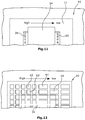
- Fig. 1 shows schematically and in cross section the essential components of the invention for a PMOS transistor 10, which is formed in this embodiment in a weakly p-doped silicon semiconductor substrate 12.
- a PMOS transistor 10 which is formed in this embodiment in a weakly p-doped silicon semiconductor substrate 12.
- the semiconductor substrate 12 there is formed an n-type well region 14 formed by ion implantation and thermal diffusion. The ion implantation occurs through the top 16 of the semiconductor substrate 12, as is conventional and known in the art.
- the actual channel region 18 of the PMOS transistor 10 is also formed.
- This channel region 18 arises as a result of ion implantation and thermal diffusion.
- On the channel region 18 there is a gate oxide layer 20 with a gate electrode 22 and possibly a metallic reinforcement 23 on this layer.
- the source connection region 24 and the drain connection region 26 are also known in principle.
- around the transistor 10 extends around a lateral insulation.
- the entire transistor region can additionally be insulated from adjacent structures of the semiconductor substrate 12 by a dielectric isolation, for example a so-called deep trench (DTI) 28.
- DTI deep trench
- a reinforced insulation 30 may in many cases also be provided for the base substrate 12 (for example by an n buried layer - NBL), which means that the transistor 10 can also be operated at potentials greatly removed from the potential of the semiconductor substrate 12 (enhanced highside ability).
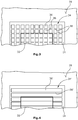
- Fig. 2 1 shows a top view of the upper side 16 of the semiconductor substrate 12 in the region of the transistor 10.
- the actual active region 32 of the transistor and the region of the n-well region 14 surrounding this region can be seen. Outside the n-well region 14, the surrounding region of the semiconductor substrate 12 to recognize.
- the n-well region 14 has a dopant concentration in the region around the active region 32 and within this active region 32. causing the PMOS transistor to have a low threshold voltage in the range of 0 volts.
- This is possible according to the invention, although in the case of ion implantation work is carried out with unchanged doses and energies which would be provided without special measures to a higher dopant concentration than in accordance with the invention in the well region 14 and thus also lead to higher threshold voltage in terms of magnitude.
- the n-well region 14 is masked out before the ion implantation, with a photoresist masking 34.
- This masking 34 comprises a multiplicity of equally distributed (masking out) regions 36 within which photoresist is located.
- another implant-preventing material may be used.
- the ion implantation now only passes into the intermediate regions 38 that are grid-shaped in this example and into the n-well region 14 to be formed.
- the dopants now also move into the areas that were previously covered by the masking areas 36.
- the dopant concentration in the n-well region 14 as a whole is reduced at the upper side 16 of the substrate 12 as compared to an n-well region that has been formed in a continuous partial region.
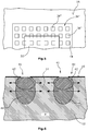
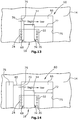
- Fig. 4 an example of an alternative trained masking 34 'is shown.
- the Ausmask ists Schemee 36 'provided with the implant blocking material are formed as elongated strips, which also elongated intermediate regions 38' arise in which the ion implantation occurs.
- FIG. 5 an example in which the masking 34 "in accordance with the embodiment according to Fig. 3 is trained. It can be seen that the implanted regions 38 "are now formed as individual fields or islands completed on all sides.
- This procedure can also be used according to the invention if a two-stage or multi-stage implantation is used as ion implantation.
- a two-stage or multi-stage implantation is used as ion implantation.
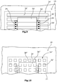
- This is in Fig. 6 indicated.
- a masking 40 is used to apply a two-stage ion implantation step.
- two dopants are introduced into two subregions 42 and 44 by exposed regions 41 of the masking 40, wherein the dopant of the subregion 44 penetrates deeper into the semiconductor substrate 12 than the dopant of the subregion 42.
- the (first) Dopant of the sub-region 42 in this case a lower mobility, ie, a shorter diffusion length, as the second dopant of the sub-area 44.
- FIG. 9 A top view of the top 16 of the semiconductor substrate 12 after processing of the semiconductor substrate according to the FIGS. 6 to 8 is in Fig. 9 shown.
- Fig. 9 In addition, the gate 54 of the MOS transistor and the source and drain terminal regions 24,26 are indicated.
- Fig. 10 shows a similar situation as in Fig. 9 , but for the masking applies that according to Fig. 5 is trained. In contrast, the masking is according to Fig. 9 around the one related to Fig. 4 is described.
- the n-well region 14 has a dopant gradient between the source terminal region 24 and the drain terminal region 26.
- This dopant profile is formed for example by a masking 60, as in Fig. 12 is shown.
- the unmasked regions 62 and 64 of different sizes can be seen, as a result of which the regions of the active region 32 not provided with ions after the ion implantation have different sizes and become larger towards the drain connection region 26.
- the dopant concentration decreases after the outdiffusion to the drain connection region 26.
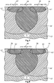
- Fig. 13 An alternative embodiment of the generation of a dopant gradient between the source terminal region 24 and the drain terminal region 26 is shown.
- the entire surrounded area active area 32 is free of ions through a masking area 66 after ion implantation.
- Adjacent to the source-side end 68 of the Gate 54 terminates Ausmask réelles Scheme 66 at a distance 70.
- the distance 70 is significantly smaller than the distance 72 between the drain-side end 74 of the gate 54 and the boundary edge 75 of Ausmask réelles Schemes 66.
- the distance 72 may be greater than the diffusion length of the dopant (s).
- the distance 70 is chosen to be significantly greater than the distance 72, then the conditions are reversed and the dopant concentration decreases starting from the later drain connection region 26 to the source connection region 24.
- both distances 70 and 72 are chosen to be approximately equal and, in particular, smaller than the diffusion length of the dopant or of the dopants, then a situation is obtained in which both the later source terminal region 24 and the drain terminal region 26 have an outdiffusion of the Masking margins 76 and 75, respectively takes place from both sides and to the same extent into the channel region 18.
- the resulting dopant concentration first decreases below the gate 54 in the direction from one of the two connection regions 24 or 26, reaches a minimum in the middle of the channel, and then increases again toward the other connection region 26 or 24 to the same extent as before has decreased.
- one of the two distances 70, 72 or even both can disappear or even become negative in the case of an expedient embodiment of the transistor, so that the channel region 18 at least at one of the two terminal regions 24, 26 the exposed, not by the Ausmasktechniks Society 66 detected surface 16 touched or even overlapped.
- the dopant concentration in the region of the source-side end 68 of the gate 54 and below this gate can be further reduced.
- a further masking area 78 is used for this purpose whose distance 80 from the masking area 66 is substantially smaller than the diffusion length. In this way, it is achieved that the dopant from the region between the two masking regions 66 and 78 also diffuses out into the region previously concealed by the masking region 78, as a result of which the amount of dopant which can now diffuse out in the direction of the channel region 18 is further reduced.
- FIGS. 15 and 16 finally show two variants in which the PMOS transistor 10 'with reduced threshold voltage is formed asymmetrically and more resistant to blocking voltage.
- both variants have a drain extension region 82 and the variant in FIG Fig. 16 additionally a field plate 84, as is conventional in itself, to offer a drift path for reducing increased reverse voltages between the drain and source of the transistor 10 '.
- This concept of the extended high-voltage capability of a PMOS transistor can thus be combined with the inventive concept of masking out during ion implantation for influencing the threshold voltage of the PMOS transistor 10 '.
Landscapes
- Insulated Gate Type Field-Effect Transistor (AREA)
Claims (7)
- Procédé de fabrication d'un transistor PMOS doté d'une tension de seuil réduite entre -0,4 Volt et +0,5 Volt, doté des étapes suivantes :- préparation d'un substrat semi-conducteur dopé type P (12) avec une face supérieure (16),- obtention d'un domaine de confinement dopé type N (14) par implantation d'un dopant N dans le substrat semi-conducteur (12) au travers de la face supérieure (16) de celui-ci,- définition d'un domaine de canal (18) sur la face supérieure (16) du substrat semi-conducteur (12) au sein du domaine de confinement (14), masquage du domaine de canal (18) au moyen d'un masque perforé comportant des échancrures sur la face supérieure (16) du substrat semi-conducteur (12),- implantation d'un ou plusieurs dopants de type N dans le domaine de canal (18) au travers des échancrures du masque perforé afin d'influer sur la tension de seuil dans un intervalle compris entre - 0,4 Volt et +0,5 Volt et- diffusion thermique des dopants des zones d'implantation de dopant introduites dans le domaine de canal (18) au travers des échancrures du masque à trous pour obtention d'une concentration en dopant essentiellement homogène ou d'une concentration en dopant inégale dans le domaine de canal (18), déterminant ainsi la tension de seuil dans un intervalle compris entre -0,4 Volt et +0,5 Volt,- définition de domaines de connexion de source et de drain (24, 26) dopés type P écartés l'un de l'autre sur la face supérieure (16) du substrat semi-conducteur (12) au sein du domaine de confinement (14).
- Procédé selon la revendication 1, doté en outre de l'étape de réalisation au sein du domaine de canal (18) de zones supplémentaires électriquement non conductrices, et ainsi par des méthodes courantes pour l'isolation des composants.
- Procédé selon la revendication 1 ou 2, doté en outre de l'étape d'élimination sur la face supérieure (16) du substrat semi-conducteur (12) des zones de celui-ci dont l'extrémité est proche des bords des échancrures, jusqu'à une profondeur pouvant être prédéfinie afin de réaliser des dépressions de surface (50), en particulier par corrosion localisée, et de l'étape de remplissage des dépressions de surface (50) du substrat semi-conducteur (12), en particulier par dépôt, avec un matériau de remplissage (52) électriquement isolant et/ou semi-conducteur, dans lequel, après le remplissage des dépressions de surface (50), le substrat semi-conducteur (12) est, en option, aplani chimiquement et/ou mécaniquement sur sa face supérieure (16).
- Procédé selon l'une des revendications 1 à 3, caractérisé en ce que l'étape d'implantation du dopant N pour influer sur la tension de seuil comprend une implantation avec différents dopants N simple ou multiple, en particulier une implantation double.
- Procédé selon la revendication 4, caractérisé en ce que les différents dopants N pénètrent dans le substrat semi-conducteur (12) à des profondeurs différentes, dans lequel il peut être prévu qu'après une étape de traitement thermique se rattachant à l'implantation multiple, le dopant N pénétrant moins profondément dans le substrat semi-conducteur (12) diffuse moins que le dopant N pénétrant plus profondément.
- Procédé selon l'une des revendications 1 à 5, caractérisé en ce que chacune des zones du substrat semi-conducteur (12) ayant une concentration de surface en dopant élevée est creusée par les dépressions de surface (50) et ainsi dont les concentrations de surface en dopant ne sont pas déterminantes pour la tension de seuil.
- Procédé selon l'une des revendications 1 à 6, caractérisé en ce qu'une zone de dérive ou d'extension (82) est réalisée dans le domaine de connexion de drain (26) et/ou entre le domaine de connexion de drain (26) et le domaine de canal (18) afin d'accroître la résistance au claquage.
Priority Applications (1)
| Application Number | Priority Date | Filing Date | Title |
|---|---|---|---|
| EP13719455.1A EP2845219B1 (fr) | 2012-05-02 | 2013-04-19 | Procédé de fabrication d'un transistor pmos à faible tension de seuil |
Applications Claiming Priority (3)
| Application Number | Priority Date | Filing Date | Title |
|---|---|---|---|
| EP12166404 | 2012-05-02 | ||
| PCT/EP2013/058188 WO2013164210A1 (fr) | 2012-05-02 | 2013-04-19 | Transistor pmos à faible tension de seuil et son procédé de fabrication |
| EP13719455.1A EP2845219B1 (fr) | 2012-05-02 | 2013-04-19 | Procédé de fabrication d'un transistor pmos à faible tension de seuil |
Publications (2)
| Publication Number | Publication Date |
|---|---|
| EP2845219A1 EP2845219A1 (fr) | 2015-03-11 |
| EP2845219B1 true EP2845219B1 (fr) | 2019-07-17 |
Family
ID=48227205
Family Applications (1)
| Application Number | Title | Priority Date | Filing Date |
|---|---|---|---|
| EP13719455.1A Active EP2845219B1 (fr) | 2012-05-02 | 2013-04-19 | Procédé de fabrication d'un transistor pmos à faible tension de seuil |
Country Status (2)
| Country | Link |
|---|---|
| EP (1) | EP2845219B1 (fr) |
| WO (1) | WO2013164210A1 (fr) |
Families Citing this family (1)
| Publication number | Priority date | Publication date | Assignee | Title |
|---|---|---|---|---|
| DE102018124740B4 (de) * | 2018-10-08 | 2025-08-28 | Infineon Technologies Ag | Verfahren zur herstellung eines halbleiterbauelements |
Family Cites Families (7)
| Publication number | Priority date | Publication date | Assignee | Title |
|---|---|---|---|---|
| DE3581348D1 (de) | 1984-09-28 | 1991-02-21 | Siemens Ag | Verfahren zum herstellen eines pn-uebergangs mit hoher durchbruchsspannung. |
| EP0389863B1 (fr) | 1989-03-29 | 1996-12-18 | Siemens Aktiengesellschaft | Procédé de fabrication d'une jonction p-n planaire à haute tenue en tension |
| US4927772A (en) | 1989-05-30 | 1990-05-22 | General Electric Company | Method of making high breakdown voltage semiconductor device |
| DE19526183C1 (de) | 1995-07-18 | 1996-09-12 | Siemens Ag | Verfahren zur Herstellung von mindestens zwei Transistoren in einem Halbleiterkörper |
| KR100220954B1 (ko) | 1996-12-31 | 1999-09-15 | 김영환 | 3중 웰을 갖는 반도체 소자 제조방법 |
| JP4703769B2 (ja) | 2009-01-15 | 2011-06-15 | 株式会社東芝 | 半導体装置及びその製造方法 |
| US8637386B2 (en) | 2009-05-12 | 2014-01-28 | Cree, Inc. | Diffused junction termination structures for silicon carbide devices and methods of fabricating silicon carbide devices incorporating same |
-
2013
- 2013-04-19 WO PCT/EP2013/058188 patent/WO2013164210A1/fr not_active Ceased
- 2013-04-19 EP EP13719455.1A patent/EP2845219B1/fr active Active
Non-Patent Citations (1)
| Title |
|---|
| None * |
Also Published As
| Publication number | Publication date |
|---|---|
| WO2013164210A1 (fr) | 2013-11-07 |
| EP2845219A1 (fr) | 2015-03-11 |
Similar Documents
| Publication | Publication Date | Title |
|---|---|---|
| DE112009000642B4 (de) | LDMOS Vorrichtungen mit verbesserten Architekturen und Herstellungsverfahren dafür | |
| EP0879481B1 (fr) | Composant semi-conducteur commande par effet de champ | |
| DE2853736C2 (de) | Feldeffektanordnung | |
| DE102008051245B4 (de) | Hochvolttransistor mit hoher Stromtragfähigkeit und Verfahren zur Herstellung | |
| DE19642538A1 (de) | Halbleitereinrichtung und Herstellungsverfahren derselben | |
| DE4219319A1 (de) | Mos-fet und herstellungsverfahren dafuer | |
| DE102006045441B4 (de) | Verfahren zur Herstellung einer Halbleiterbauelementanordnung mit einer Trenchtransistorstruktur | |
| DE112005000441T5 (de) | Halbleiterbauteil und Verfahren zur Herstellung desselben | |
| DE102004009521B4 (de) | Hochvolt-PMOS-Transistor, Maske zur Herstellung einer Wanne und Verfahren zur Herstellung eines Hochvolt-PMOS-Transistors | |
| WO1997013277A1 (fr) | Transistor mos a haute rigidite dielectrique de sortie | |
| EP0973204A2 (fr) | Transistor MOS avec tension de claquage élevée et resistance passante reduite | |
| EP0973205B1 (fr) | Transistor de type MOS haute tension | |
| DE2729657A1 (de) | Feldeffekttransistor mit extrem kurzer kanallaenge | |
| EP2845219B1 (fr) | Procédé de fabrication d'un transistor pmos à faible tension de seuil | |
| DE102006007096B4 (de) | MOSFET mit Kompensationsstruktur und Randabschluss sowie Verfahren zu dessen Herstellung | |
| WO2007033692A1 (fr) | Transistor haute tension et procede de realisation | |
| DE10361135B4 (de) | Trenchtransistor und Verfahren zur Herstellung eines Trenchtransistors mit hochenergieimplantiertem Drain | |
| DE102004014928B4 (de) | Hochvolttransistor und Verfahren zu seiner Herstellung | |
| DE102004063991B4 (de) | Verfahren zur Herstellung von dotierten Halbleitergebieten in einem Halbleiterkörper eines lateralen Trenchtransistors | |
| DE102005048000B4 (de) | Verfahren zur Herstellung eines Transistors mit zuverlässiger Source-Dotierung | |
| DE10235000B4 (de) | Verfahren zur Bildung einer Kanalzone eines Transistors und NMOS-Transistor | |
| DE4322549C2 (de) | MOS-Transistor mit hoher Ausgangsspannungsfestigkeit | |
| DE102006012447B4 (de) | Verfahren zur Herstellung einer Transistorstruktur | |
| EP1670052B1 (fr) | Méthode de fabrication d'un dispositif semi-conducteur comportant une structure semi-conductrice à PMOSFET à tenue en tension et une structure semi-conductrice à NMOSFET | |
| DE10002129B4 (de) | Vertikale DMOS-Transistoranordnung mit niedrigem Einschaltwiderstand |
Legal Events
| Date | Code | Title | Description |
|---|---|---|---|
| PUAI | Public reference made under article 153(3) epc to a published international application that has entered the european phase |
Free format text: ORIGINAL CODE: 0009012 |
|
| 17P | Request for examination filed |
Effective date: 20141125 |
|
| AK | Designated contracting states |
Kind code of ref document: A1 Designated state(s): AL AT BE BG CH CY CZ DE DK EE ES FI FR GB GR HR HU IE IS IT LI LT LU LV MC MK MT NL NO PL PT RO RS SE SI SK SM TR |
|
| AX | Request for extension of the european patent |
Extension state: BA ME |
|
| DAX | Request for extension of the european patent (deleted) | ||
| RAP1 | Party data changed (applicant data changed or rights of an application transferred) |
Owner name: ELMOS SEMICONDUCTOR AKTIENGESELLSCHAFT |
|
| RAP1 | Party data changed (applicant data changed or rights of an application transferred) |
Owner name: ELMOS SEMICONDUCTOR AKTIENGESELLSCHAFT |
|
| STAA | Information on the status of an ep patent application or granted ep patent |
Free format text: STATUS: EXAMINATION IS IN PROGRESS |
|
| 17Q | First examination report despatched |
Effective date: 20170220 |
|
| GRAP | Despatch of communication of intention to grant a patent |
Free format text: ORIGINAL CODE: EPIDOSNIGR1 |
|
| STAA | Information on the status of an ep patent application or granted ep patent |
Free format text: STATUS: GRANT OF PATENT IS INTENDED |
|
| RIC1 | Information provided on ipc code assigned before grant |
Ipc: H01L 21/266 20060101AFI20190107BHEP Ipc: H01L 29/78 20060101ALI20190107BHEP Ipc: H01L 29/10 20060101ALI20190107BHEP |
|
| INTG | Intention to grant announced |
Effective date: 20190128 |
|
| RIN1 | Information on inventor provided before grant (corrected) |
Inventor name: ROTTER, THOMAS |
|
| GRAS | Grant fee paid |
Free format text: ORIGINAL CODE: EPIDOSNIGR3 |
|
| GRAA | (expected) grant |
Free format text: ORIGINAL CODE: 0009210 |
|
| STAA | Information on the status of an ep patent application or granted ep patent |
Free format text: STATUS: THE PATENT HAS BEEN GRANTED |
|
| AK | Designated contracting states |
Kind code of ref document: B1 Designated state(s): AL AT BE BG CH CY CZ DE DK EE ES FI FR GB GR HR HU IE IS IT LI LT LU LV MC MK MT NL NO PL PT RO RS SE SI SK SM TR |
|
| REG | Reference to a national code |
Ref country code: GB Ref legal event code: FG4D Free format text: NOT ENGLISH |
|
| REG | Reference to a national code |
Ref country code: CH Ref legal event code: EP |
|
| REG | Reference to a national code |
Ref country code: IE Ref legal event code: FG4D Free format text: LANGUAGE OF EP DOCUMENT: GERMAN |
|
| REG | Reference to a national code |
Ref country code: DE Ref legal event code: R096 Ref document number: 502013013176 Country of ref document: DE |
|
| REG | Reference to a national code |
Ref country code: AT Ref legal event code: REF Ref document number: 1156617 Country of ref document: AT Kind code of ref document: T Effective date: 20190815 |
|
| REG | Reference to a national code |
Ref country code: NL Ref legal event code: MP Effective date: 20190717 |
|
| REG | Reference to a national code |
Ref country code: LT Ref legal event code: MG4D |
|
| PG25 | Lapsed in a contracting state [announced via postgrant information from national office to epo] |
Ref country code: BG Free format text: LAPSE BECAUSE OF FAILURE TO SUBMIT A TRANSLATION OF THE DESCRIPTION OR TO PAY THE FEE WITHIN THE PRESCRIBED TIME-LIMIT Effective date: 20191017 Ref country code: NO Free format text: LAPSE BECAUSE OF FAILURE TO SUBMIT A TRANSLATION OF THE DESCRIPTION OR TO PAY THE FEE WITHIN THE PRESCRIBED TIME-LIMIT Effective date: 20191017 Ref country code: LT Free format text: LAPSE BECAUSE OF FAILURE TO SUBMIT A TRANSLATION OF THE DESCRIPTION OR TO PAY THE FEE WITHIN THE PRESCRIBED TIME-LIMIT Effective date: 20190717 Ref country code: FI Free format text: LAPSE BECAUSE OF FAILURE TO SUBMIT A TRANSLATION OF THE DESCRIPTION OR TO PAY THE FEE WITHIN THE PRESCRIBED TIME-LIMIT Effective date: 20190717 Ref country code: PT Free format text: LAPSE BECAUSE OF FAILURE TO SUBMIT A TRANSLATION OF THE DESCRIPTION OR TO PAY THE FEE WITHIN THE PRESCRIBED TIME-LIMIT Effective date: 20191118 Ref country code: NL Free format text: LAPSE BECAUSE OF FAILURE TO SUBMIT A TRANSLATION OF THE DESCRIPTION OR TO PAY THE FEE WITHIN THE PRESCRIBED TIME-LIMIT Effective date: 20190717 Ref country code: SE Free format text: LAPSE BECAUSE OF FAILURE TO SUBMIT A TRANSLATION OF THE DESCRIPTION OR TO PAY THE FEE WITHIN THE PRESCRIBED TIME-LIMIT Effective date: 20190717 Ref country code: HR Free format text: LAPSE BECAUSE OF FAILURE TO SUBMIT A TRANSLATION OF THE DESCRIPTION OR TO PAY THE FEE WITHIN THE PRESCRIBED TIME-LIMIT Effective date: 20190717 |
|
| PG25 | Lapsed in a contracting state [announced via postgrant information from national office to epo] |
Ref country code: GR Free format text: LAPSE BECAUSE OF FAILURE TO SUBMIT A TRANSLATION OF THE DESCRIPTION OR TO PAY THE FEE WITHIN THE PRESCRIBED TIME-LIMIT Effective date: 20191018 Ref country code: LV Free format text: LAPSE BECAUSE OF FAILURE TO SUBMIT A TRANSLATION OF THE DESCRIPTION OR TO PAY THE FEE WITHIN THE PRESCRIBED TIME-LIMIT Effective date: 20190717 Ref country code: AL Free format text: LAPSE BECAUSE OF FAILURE TO SUBMIT A TRANSLATION OF THE DESCRIPTION OR TO PAY THE FEE WITHIN THE PRESCRIBED TIME-LIMIT Effective date: 20190717 Ref country code: RS Free format text: LAPSE BECAUSE OF FAILURE TO SUBMIT A TRANSLATION OF THE DESCRIPTION OR TO PAY THE FEE WITHIN THE PRESCRIBED TIME-LIMIT Effective date: 20190717 Ref country code: IS Free format text: LAPSE BECAUSE OF FAILURE TO SUBMIT A TRANSLATION OF THE DESCRIPTION OR TO PAY THE FEE WITHIN THE PRESCRIBED TIME-LIMIT Effective date: 20191117 Ref country code: ES Free format text: LAPSE BECAUSE OF FAILURE TO SUBMIT A TRANSLATION OF THE DESCRIPTION OR TO PAY THE FEE WITHIN THE PRESCRIBED TIME-LIMIT Effective date: 20190717 |
|
| PG25 | Lapsed in a contracting state [announced via postgrant information from national office to epo] |
Ref country code: TR Free format text: LAPSE BECAUSE OF FAILURE TO SUBMIT A TRANSLATION OF THE DESCRIPTION OR TO PAY THE FEE WITHIN THE PRESCRIBED TIME-LIMIT Effective date: 20190717 |
|
| PG25 | Lapsed in a contracting state [announced via postgrant information from national office to epo] |
Ref country code: IT Free format text: LAPSE BECAUSE OF FAILURE TO SUBMIT A TRANSLATION OF THE DESCRIPTION OR TO PAY THE FEE WITHIN THE PRESCRIBED TIME-LIMIT Effective date: 20190717 Ref country code: DK Free format text: LAPSE BECAUSE OF FAILURE TO SUBMIT A TRANSLATION OF THE DESCRIPTION OR TO PAY THE FEE WITHIN THE PRESCRIBED TIME-LIMIT Effective date: 20190717 Ref country code: PL Free format text: LAPSE BECAUSE OF FAILURE TO SUBMIT A TRANSLATION OF THE DESCRIPTION OR TO PAY THE FEE WITHIN THE PRESCRIBED TIME-LIMIT Effective date: 20190717 Ref country code: EE Free format text: LAPSE BECAUSE OF FAILURE TO SUBMIT A TRANSLATION OF THE DESCRIPTION OR TO PAY THE FEE WITHIN THE PRESCRIBED TIME-LIMIT Effective date: 20190717 Ref country code: RO Free format text: LAPSE BECAUSE OF FAILURE TO SUBMIT A TRANSLATION OF THE DESCRIPTION OR TO PAY THE FEE WITHIN THE PRESCRIBED TIME-LIMIT Effective date: 20190717 |
|
| PG25 | Lapsed in a contracting state [announced via postgrant information from national office to epo] |
Ref country code: CZ Free format text: LAPSE BECAUSE OF FAILURE TO SUBMIT A TRANSLATION OF THE DESCRIPTION OR TO PAY THE FEE WITHIN THE PRESCRIBED TIME-LIMIT Effective date: 20190717 Ref country code: SM Free format text: LAPSE BECAUSE OF FAILURE TO SUBMIT A TRANSLATION OF THE DESCRIPTION OR TO PAY THE FEE WITHIN THE PRESCRIBED TIME-LIMIT Effective date: 20190717 Ref country code: IS Free format text: LAPSE BECAUSE OF FAILURE TO SUBMIT A TRANSLATION OF THE DESCRIPTION OR TO PAY THE FEE WITHIN THE PRESCRIBED TIME-LIMIT Effective date: 20200224 Ref country code: SK Free format text: LAPSE BECAUSE OF FAILURE TO SUBMIT A TRANSLATION OF THE DESCRIPTION OR TO PAY THE FEE WITHIN THE PRESCRIBED TIME-LIMIT Effective date: 20190717 |
|
| REG | Reference to a national code |
Ref country code: DE Ref legal event code: R097 Ref document number: 502013013176 Country of ref document: DE |
|
| PLBE | No opposition filed within time limit |
Free format text: ORIGINAL CODE: 0009261 |
|
| STAA | Information on the status of an ep patent application or granted ep patent |
Free format text: STATUS: NO OPPOSITION FILED WITHIN TIME LIMIT |
|
| PG2D | Information on lapse in contracting state deleted |
Ref country code: IS |
|
| REG | Reference to a national code |
Ref country code: DE Ref legal event code: R082 Ref document number: 502013013176 Country of ref document: DE Representative=s name: DOMPATENT VON KREISLER SELTING WERNER - PARTNE, DE Ref country code: DE Ref legal event code: R081 Ref document number: 502013013176 Country of ref document: DE Owner name: ELMOS SEMICONDUCTOR SE, DE Free format text: FORMER OWNER: ELMOS SEMICONDUCTOR AKTIENGESELLSCHAFT, 44227 DORTMUND, DE |
|
| 26N | No opposition filed |
Effective date: 20200603 |
|
| PG25 | Lapsed in a contracting state [announced via postgrant information from national office to epo] |
Ref country code: SI Free format text: LAPSE BECAUSE OF FAILURE TO SUBMIT A TRANSLATION OF THE DESCRIPTION OR TO PAY THE FEE WITHIN THE PRESCRIBED TIME-LIMIT Effective date: 20190717 |
|
| PG25 | Lapsed in a contracting state [announced via postgrant information from national office to epo] |
Ref country code: MC Free format text: LAPSE BECAUSE OF FAILURE TO SUBMIT A TRANSLATION OF THE DESCRIPTION OR TO PAY THE FEE WITHIN THE PRESCRIBED TIME-LIMIT Effective date: 20190717 |
|
| REG | Reference to a national code |
Ref country code: CH Ref legal event code: PL |
|
| PG25 | Lapsed in a contracting state [announced via postgrant information from national office to epo] |
Ref country code: LU Free format text: LAPSE BECAUSE OF NON-PAYMENT OF DUE FEES Effective date: 20200419 Ref country code: FR Free format text: LAPSE BECAUSE OF NON-PAYMENT OF DUE FEES Effective date: 20200430 Ref country code: LI Free format text: LAPSE BECAUSE OF NON-PAYMENT OF DUE FEES Effective date: 20200430 Ref country code: CH Free format text: LAPSE BECAUSE OF NON-PAYMENT OF DUE FEES Effective date: 20200430 |
|
| REG | Reference to a national code |
Ref country code: BE Ref legal event code: MM Effective date: 20200430 |
|
| PG25 | Lapsed in a contracting state [announced via postgrant information from national office to epo] |
Ref country code: BE Free format text: LAPSE BECAUSE OF NON-PAYMENT OF DUE FEES Effective date: 20200430 |
|
| GBPC | Gb: european patent ceased through non-payment of renewal fee |
Effective date: 20200419 |
|
| PG25 | Lapsed in a contracting state [announced via postgrant information from national office to epo] |
Ref country code: IE Free format text: LAPSE BECAUSE OF NON-PAYMENT OF DUE FEES Effective date: 20200419 Ref country code: GB Free format text: LAPSE BECAUSE OF NON-PAYMENT OF DUE FEES Effective date: 20200419 |
|
| REG | Reference to a national code |
Ref country code: AT Ref legal event code: MM01 Ref document number: 1156617 Country of ref document: AT Kind code of ref document: T Effective date: 20200419 |
|
| PG25 | Lapsed in a contracting state [announced via postgrant information from national office to epo] |
Ref country code: AT Free format text: LAPSE BECAUSE OF NON-PAYMENT OF DUE FEES Effective date: 20200419 |
|
| PG25 | Lapsed in a contracting state [announced via postgrant information from national office to epo] |
Ref country code: MT Free format text: LAPSE BECAUSE OF FAILURE TO SUBMIT A TRANSLATION OF THE DESCRIPTION OR TO PAY THE FEE WITHIN THE PRESCRIBED TIME-LIMIT Effective date: 20190717 Ref country code: CY Free format text: LAPSE BECAUSE OF FAILURE TO SUBMIT A TRANSLATION OF THE DESCRIPTION OR TO PAY THE FEE WITHIN THE PRESCRIBED TIME-LIMIT Effective date: 20190717 |
|
| PG25 | Lapsed in a contracting state [announced via postgrant information from national office to epo] |
Ref country code: MK Free format text: LAPSE BECAUSE OF FAILURE TO SUBMIT A TRANSLATION OF THE DESCRIPTION OR TO PAY THE FEE WITHIN THE PRESCRIBED TIME-LIMIT Effective date: 20190717 |
|
| P01 | Opt-out of the competence of the unified patent court (upc) registered |
Effective date: 20230525 |
|
| PGFP | Annual fee paid to national office [announced via postgrant information from national office to epo] |
Ref country code: DE Payment date: 20250415 Year of fee payment: 13 |
|
| REG | Reference to a national code |
Ref country code: DE Ref legal event code: R081 Ref document number: 502013013176 Country of ref document: DE Owner name: ELMOS SEMICONDUCTOR SE, DE Free format text: FORMER OWNER: ELMOS SEMICONDUCTOR SE, 44227 DORTMUND, DE |
|
| REG | Reference to a national code |
Ref country code: DE Ref legal event code: R079 Ref document number: 502013013176 Country of ref document: DE Free format text: PREVIOUS MAIN CLASS: H01L0021266000 Ipc: H10P0030220000 |