EP2846353B1 - Procédé de fabrication d'un dispositif à semi-conducteur à oxyde de métal complémentaire - Google Patents
Procédé de fabrication d'un dispositif à semi-conducteur à oxyde de métal complémentaire Download PDFInfo
- Publication number
- EP2846353B1 EP2846353B1 EP14183431.7A EP14183431A EP2846353B1 EP 2846353 B1 EP2846353 B1 EP 2846353B1 EP 14183431 A EP14183431 A EP 14183431A EP 2846353 B1 EP2846353 B1 EP 2846353B1
- Authority
- EP
- European Patent Office
- Prior art keywords
- layer
- type transistor
- manufacturing
- buffer layer
- pattern
- Prior art date
- Legal status (The legal status is an assumption and is not a legal conclusion. Google has not performed a legal analysis and makes no representation as to the accuracy of the status listed.)
- Active
Links
Images



Classifications
-
- H—ELECTRICITY
- H10—SEMICONDUCTOR DEVICES; ELECTRIC SOLID-STATE DEVICES NOT OTHERWISE PROVIDED FOR
- H10D—INORGANIC ELECTRIC SEMICONDUCTOR DEVICES
- H10D84/00—Integrated devices formed in or on semiconductor substrates that comprise only semiconducting layers, e.g. on Si wafers or on GaAs-on-Si wafers
- H10D84/01—Manufacture or treatment
- H10D84/02—Manufacture or treatment characterised by using material-based technologies
- H10D84/05—Manufacture or treatment characterised by using material-based technologies using Group III-V technology
-
- H—ELECTRICITY
- H10—SEMICONDUCTOR DEVICES; ELECTRIC SOLID-STATE DEVICES NOT OTHERWISE PROVIDED FOR
- H10D—INORGANIC ELECTRIC SEMICONDUCTOR DEVICES
- H10D84/00—Integrated devices formed in or on semiconductor substrates that comprise only semiconducting layers, e.g. on Si wafers or on GaAs-on-Si wafers
- H10D84/01—Manufacture or treatment
- H10D84/0123—Integrating together multiple components covered by H10D12/00 or H10D30/00, e.g. integrating multiple IGBTs
- H10D84/0126—Integrating together multiple components covered by H10D12/00 or H10D30/00, e.g. integrating multiple IGBTs the components including insulated gates, e.g. IGFETs
- H10D84/0165—Integrating together multiple components covered by H10D12/00 or H10D30/00, e.g. integrating multiple IGBTs the components including insulated gates, e.g. IGFETs the components including complementary IGFETs, e.g. CMOS devices
-
- H—ELECTRICITY
- H10—SEMICONDUCTOR DEVICES; ELECTRIC SOLID-STATE DEVICES NOT OTHERWISE PROVIDED FOR
- H10D—INORGANIC ELECTRIC SEMICONDUCTOR DEVICES
- H10D84/00—Integrated devices formed in or on semiconductor substrates that comprise only semiconducting layers, e.g. on Si wafers or on GaAs-on-Si wafers
- H10D84/01—Manufacture or treatment
-
- H—ELECTRICITY
- H10—SEMICONDUCTOR DEVICES; ELECTRIC SOLID-STATE DEVICES NOT OTHERWISE PROVIDED FOR
- H10D—INORGANIC ELECTRIC SEMICONDUCTOR DEVICES
- H10D84/00—Integrated devices formed in or on semiconductor substrates that comprise only semiconducting layers, e.g. on Si wafers or on GaAs-on-Si wafers
- H10D84/01—Manufacture or treatment
- H10D84/02—Manufacture or treatment characterised by using material-based technologies
- H10D84/03—Manufacture or treatment characterised by using material-based technologies using Group IV technology, e.g. silicon technology or silicon-carbide [SiC] technology
- H10D84/038—Manufacture or treatment characterised by using material-based technologies using Group IV technology, e.g. silicon technology or silicon-carbide [SiC] technology using silicon technology, e.g. SiGe
-
- H—ELECTRICITY
- H10—SEMICONDUCTOR DEVICES; ELECTRIC SOLID-STATE DEVICES NOT OTHERWISE PROVIDED FOR
- H10D—INORGANIC ELECTRIC SEMICONDUCTOR DEVICES
- H10D84/00—Integrated devices formed in or on semiconductor substrates that comprise only semiconducting layers, e.g. on Si wafers or on GaAs-on-Si wafers
- H10D84/80—Integrated devices formed in or on semiconductor substrates that comprise only semiconducting layers, e.g. on Si wafers or on GaAs-on-Si wafers characterised by the integration of at least one component covered by groups H10D12/00 or H10D30/00, e.g. integration of IGFETs
- H10D84/82—Integrated devices formed in or on semiconductor substrates that comprise only semiconducting layers, e.g. on Si wafers or on GaAs-on-Si wafers characterised by the integration of at least one component covered by groups H10D12/00 or H10D30/00, e.g. integration of IGFETs of only field-effect components
- H10D84/83—Integrated devices formed in or on semiconductor substrates that comprise only semiconducting layers, e.g. on Si wafers or on GaAs-on-Si wafers characterised by the integration of at least one component covered by groups H10D12/00 or H10D30/00, e.g. integration of IGFETs of only field-effect components of only insulated-gate FETs [IGFET]
- H10D84/8311—Integrated devices formed in or on semiconductor substrates that comprise only semiconducting layers, e.g. on Si wafers or on GaAs-on-Si wafers characterised by the integration of at least one component covered by groups H10D12/00 or H10D30/00, e.g. integration of IGFETs of only field-effect components of only insulated-gate FETs [IGFET] the IGFETs characterised by having different channel structures
-
- H—ELECTRICITY
- H10—SEMICONDUCTOR DEVICES; ELECTRIC SOLID-STATE DEVICES NOT OTHERWISE PROVIDED FOR
- H10D—INORGANIC ELECTRIC SEMICONDUCTOR DEVICES
- H10D84/00—Integrated devices formed in or on semiconductor substrates that comprise only semiconducting layers, e.g. on Si wafers or on GaAs-on-Si wafers
- H10D84/80—Integrated devices formed in or on semiconductor substrates that comprise only semiconducting layers, e.g. on Si wafers or on GaAs-on-Si wafers characterised by the integration of at least one component covered by groups H10D12/00 or H10D30/00, e.g. integration of IGFETs
- H10D84/82—Integrated devices formed in or on semiconductor substrates that comprise only semiconducting layers, e.g. on Si wafers or on GaAs-on-Si wafers characterised by the integration of at least one component covered by groups H10D12/00 or H10D30/00, e.g. integration of IGFETs of only field-effect components
- H10D84/83—Integrated devices formed in or on semiconductor substrates that comprise only semiconducting layers, e.g. on Si wafers or on GaAs-on-Si wafers characterised by the integration of at least one component covered by groups H10D12/00 or H10D30/00, e.g. integration of IGFETs of only field-effect components of only insulated-gate FETs [IGFET]
- H10D84/85—Complementary IGFETs, e.g. CMOS
-
- H—ELECTRICITY
- H10—SEMICONDUCTOR DEVICES; ELECTRIC SOLID-STATE DEVICES NOT OTHERWISE PROVIDED FOR
- H10D—INORGANIC ELECTRIC SEMICONDUCTOR DEVICES
- H10D84/00—Integrated devices formed in or on semiconductor substrates that comprise only semiconducting layers, e.g. on Si wafers or on GaAs-on-Si wafers
- H10D84/01—Manufacture or treatment
- H10D84/02—Manufacture or treatment characterised by using material-based technologies
- H10D84/08—Manufacture or treatment characterised by using material-based technologies using combinations of technologies, e.g. using both Si and SiC technologies or using both Si and Group III-V technologies
Definitions
- CMOS complementary metal oxide semiconductor
- Group III-V semiconductor materials Since the electron mobility of Group III-V compound semiconductor materials is higher by about 10 times to about 10 3 times than the electron mobility of silicon (Si), the Group III-V compound semiconductor materials are used for high-speed channels in complementary metal oxide semiconductor (CMOS) devices or are suitably applied to high-efficiency Group III-V solar cells.
- CMOS complementary metal oxide semiconductor
- the Group III-V substrates are more expensive and more likely to be damaged during a process than Si substrates.
- the maximum size of commercial substrates is about 6 inches, and the Group III-V substrates are difficult to manufacture in large sizes.
- semiconductor devices using Si substrates instead of Group III-V substrates have been developed.
- US 2013/0062696 and US 2013/0246409 describe methods of preparing a SOI semiconductor structure with a hybrid of coplanar Ge and III-V.
- a first aspect of the invention relates to methods of manufacturing CMOS devices including both an n-type transistor layer and a p-type transistor layer on a silicon substrate according to claim 1.
- a CMOS device includes a silicon substrate; a buffer layer on the silicon substrate; a first layer for an n-type transistor on the buffer layer; a second layer for a p-type transistor disposed on the buffer layer or the silicon substrate while being spaced apart from the first layer; and an insulating layer between the first layer and the second layer.
- At least one example embodiment includes a method of manufacturing a complementary metal oxide semiconductor (CMOS) device that includes forming a buffer layer on a substrate, forming a first material layer on the buffer layer, the first material layer including a group III-V material, etching the first material layer to form a first layer and a first pattern, forming an insulating layer on the first layer and the first pattern, etching the insulating layer to form a second pattern, and selectively growing a second material layer in the second pattern, the second material layer including a group IV material.
- CMOS complementary metal oxide semiconductor
- a method of manufacturing a complementary metal oxide semiconductor (CMOS) device includes forming a buffer layer on a silicon substrate; forming a material layer for an n-type transistor on the buffer layer; etching the material layer for the n-type transistor to form a first layer for the n-type transistor and a first pattern; forming an insulating layer on the first layer and the first pattern; etching the insulating layer to form a second pattern for selective growth; and selectively growing a second layer for a p-type transistor in the second pattern.
- CMOS complementary metal oxide semiconductor
- the buffer layer may include or, alternatively, be formed of a Group III-V material including at least one selected from the group consisting of indium (In), gallium (Ga), and aluminum (Al), and at least one selected from the group consisting of arsenic (As), phosphorus (P), and antimony (Sb).
- a Group III-V material including at least one selected from the group consisting of indium (In), gallium (Ga), and aluminum (Al), and at least one selected from the group consisting of arsenic (As), phosphorus (P), and antimony (Sb).
- the buffer layer may include or, alternatively, be formed of at least one selected from the group consisting of InP, InAs, InSb, GaAs, GaP, GaSb, AlP, AlAs, AlSb, InAlAs, InGaP, GaAsP, InGaAsP, and InGaAlAs.
- the buffer layer may be doped with an n-type dopant.
- the buffer layer may include at least one Group IV material.
- the buffer layer may include or, alternatively, be formed of at least one of SiGe, GeSn, and germanium (Ge).
- the first layer may include or, alternatively, be formed of a Group III-V material.
- the first layer may include or, alternatively, be formed of at least one of InGaAs, InP, InSb, InGaSb, GaSb, and InAs.
- the second layer may include or, alternatively, be formed of a Group IV material.
- the second layer may include or, alternatively, be formed of Ge.
- the n-type transistor may include an n-type metal oxide semiconductor field effect transistor (MOSFET).
- MOSFET metal oxide semiconductor field effect transistor
- the p-type transistor may include a p-type MOSFET.
- the first layer and the second layer may be channel layers.
- the material layer may be etched to expose a portion of the buffer layer.
- the material layer may be etched to expose the silicon substrate.
- the insulating layer may include or, alternatively, be formed of a silicon oxide film, a silicon nitride film, or a silicon oxynitride film.
- CMOS complementary metal oxide semiconductor
- first, second, etc. may be used herein to describe various elements, components, regions, layers and/or sections, these elements, components, regions, layers and/or sections should not be limited by these terms. These terms are only used to distinguish one element, component, region, layer or section from another element, component, region, layer or section. Thus, a first element, component, region, layer or section discussed below could be termed a second element, component, region, layer or section without departing from the teachings of example embodiments.
- spatially relative terms such as “beneath,” “below,” “lower,” “above,” “upper” and the like, may be used herein for ease of description to describe one element or feature's relationship to another element(s) or feature(s) as illustrated in the figures. It will be understood that the spatially relative terms are intended to encompass different orientations of the device in use or operation in addition to the orientation depicted in the figures. For example, if the device in the figures is turned over, elements described as “below” or “beneath” other elements or features would then be oriented “above” the other elements or features. Thus, the example term “below” can encompass both an orientation of above and below. The device may be otherwise oriented (rotated 90 degrees or at other orientations) and the spatially relative descriptors used herein interpreted accordingly.
- Example embodiments are described herein with reference to cross-sectional illustrations that are schematic illustrations of idealized embodiments (and intermediate structures) of example embodiments. As such, variations from the shapes of the illustrations as a result, for example, of manufacturing techniques and/or tolerances, are to be expected. Thus, example embodiments should not be construed as limited to the particular shapes of regions illustrated herein but are to include deviations in shapes that result, for example, from manufacturing. For example, an implanted region illustrated as a rectangle will, typically, have rounded or curved features and/or a gradient of implant concentration at its edges rather than a binary change from implanted to non-implanted region.
- a buried region formed by implantation may result in some implantation in the region between the buried region and the surface through which the implantation takes place.
- the regions illustrated in the figures are schematic in nature and their shapes are not intended to illustrate the actual shape of a region of a device and are not intended to limit the scope of example embodiments.
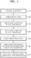
- FIG. 1 is a flowchart illustrating a CMOS device manufacturing method according to an example embodiment.
- a substrate is prepared S10, and a buffer layer is formed on the substrate S20.
- the substrate may be a silicon-based substrate.
- the substrate may be a silicon substrate.
- a first layer for an n-type transistor is grown on the buffer layer S30.
- the n-type transistor may be an n-type metal oxide semiconductor field effect transistor (MOSFET).
- MOSFET metal oxide semiconductor field effect transistor
- the first layer for the n-type transistor is etched to form a first pattern S40.
- the first pattern may expose a portion of the buffer layer or may expose a portion of the substrate.
- An insulating layer is stacked on the first layer for the n-type transistor and the first pattern S50.
- the insulating layer is etched to form a second pattern for selective growth S60.
- the second pattern may be a pattern for selectively growing a second layer for a p-type transistor.
- a second layer for a p-type transistor is formed in the second pattern S70.
- the p-type transistor may be a p-type MOSFET.
- the first layer for the n-type transistor may be formed of a material with high electron mobility
- the second layer for the p-type transistor may be formed of a material with high hole mobility.
- the example embodiment provides a manufacturing method that may form both an n-type transistor and a p-type transistor on one substrate.
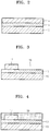
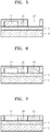
- FIGS. 2 to 8 illustrate a CMOS device manufacturing method according to an example embodiment.
- a buffer layer 13 may be formed on a substrate 10, and a material layer 15 for an n-type transistor may be formed on the buffer layer 13.
- the substrate 10 may be a silicon-based substrate.
- the substrate 10 may be doped with a p-type or n-type dopant.
- the substrate 10 may be a silicon substrate, and may be a p-type silicon substrate.
- the material layer 15 for the n-type transistor may be formed of a Group III-V material, which will be described later.
- the buffer layer 13 may be formed of a Group III-V material of the same series as the material layer 15.
- the buffer layer 13 may include a Group III-V material including at least one selected from the group consisting of indium (In), gallium (Ga), and aluminum (Al), and at least one selected from the group consisting of arsenic (As), phosphorus (P), and antimony (Sb).
- the Group III-V material for the buffer layer 13 may be a two-element material, a three-element material, or a four-element material.
- the two-element material may be InP, InAs, InSb, GaAs, GaP, GaSb, AlP, AlAs, or AlSb.
- the three-element material may be InAlAs, InGaP, or GaAsP.
- the four-element material may be InGaAsP or InGaAlAs.
- the buffer layer 13 may be an n-type material layer.
- the buffer layer 13 may be a layer doped with an n-type dopant, or may be a layer having an n-type doping effect.
- the buffer layer 13 may be an n-InP layer.
- the buffer layer 13 may reduce the lattice constant difference and the thermal expansion coefficient difference between the substrate 10 and the material layer 15 for the n-type transistor and reduce the defects thereof to increase the crystallinity of the material layer 15 of the n-type transistor.
- the buffer layer 13 may be formed of a material of the same series as a material for a second layer 25 for a p-type transistor, which will be described later.
- the buffer layer 13 may be formed of at least one Group IV material.
- the buffer layer 13 may include at least one of SiGe, GeSn, and Ge.
- the material layer 15 for the n-type transistor may be formed of a Group III-V material.
- the III-V material may include at least one of InGaAs, InP, InSb, InGaSb, GaSb, and InAs.
- the material layer 15 for the n-type transistor may have a quantum well structure.
- a wet treatment or in-situ annealing may be performed as a pretreatment on the material layer 15 of the n-type transistor.
- the n-type transistor may be an n-type MOSFET.
- the material layer 15 for the n-type transistor may be etched to form a first layer 17 for the n-type transistor and a first pattern 18.
- the first layer 17 may be a channel layer of the n-type transistor.
- the first pattern 18 may expose a portion of the buffer layer 13.
- the material layer 15 for the n-type transistor may be etched by using photoresist.
- an insulating layer 20 may be formed on the first layer 17 for the n-type transistor and an exposed region of the buffer layer 13.
- the insulating layer 20 may be formed of an oxide film, a nitride film, or an oxynitride film.
- the insulating layer 20 may be formed of a silicon oxide (SiO 2 ) film, a silicon nitride (SiN x ) film, or a silicon oxynitride (SiO x N y ) film. Referring to FIG.
- the insulating layer 20 may be etched to form a second pattern 23 for selective growth.
- a second layer 25 for a p-type transistor may be formed in the second pattern 23 by selective growth.
- the second layer 25 may be grown to have a thickness that is smaller than, equal to, or greater than the depth of the second pattern 23.
- the surface of the second layer 25 may be planarized through a planarization process.
- the planarization process may be a chemical mechanical polishing (CMP) process.
- CMP chemical mechanical polishing
- the planarization process is not mandatory but may be performed selectively according to the surface state of the second layer 25.
- the insulating layer 20 may be used as a mask in the selective growth process.
- the second layer 25 may be formed of a material including a Group IV material.
- the second layer 25 may be formed of germanium (Ge).
- the second layer 25 may be grown by epitaxial growth.
- the second layer 25 may be formed by growing germanium to several tens of nm at a low temperature of, for example, about 400°C, and then growing germanium at a high temperature of, for example, about 600°C.
- the insulating layer 20 may be used as a mask. Since the surface of the first layer 17 is covered with the insulating layer 20, the second layer 25 may be selectively grown on the exposed region of the buffer layer 13.
- the surface of the resulting structure illustrated in FIG. 6 may be planarized to expose the first layer 17.
- the planarization may be performed through a CMP process.
- both the first layer 17 for the n-type transistor and the second layer 25 for the p-type transistor may be formed on one substrate 10.
- selectively growing the second layer 25 formed of a Ge material may be easier and simpler than selectively growing the first layer 17 formed of a Group III-V material.
- a first source electrode S1 and a first drain electrode D1 may be formed at both sides of the first layer 17.
- the first source electrode S1 and the first drain electrode D1 may be formed at a top portion of the first layer 17 while being spaced apart from each other.
- a second source electrode S2 and a second drain electrode D2 may be formed at both sides of the second layer 25.
- the second source electrode S2 and the second drain electrode D2 may be formed at a top portion of the second layer 25 while being spaced apart from each other.
- the first and second source electrodes S1 and S2 and the first and second drain electrodes D1 and D2 may be formed by implantation.
- the source electrodes and the drain electrodes may be formed by various other methods.
- the first and second source electrodes S1 and S2 and the first and second drain electrodes D1 and D2 may be formed of a conductive material, for example, a metal or an alloy.
- the first and second source electrodes S1 and S2 and the first and second drain electrodes D1 and D2 may be formed of a Ti/Au alloy or a Ge/Au/Ni/Au alloy.
- a first gate insulating layer 30 may be formed on the first layer 17, and a second gate insulating layer 40 may be formed on the second layer 25.
- the first and second gate insulating layers 30 and 40 may include at least one of Al 2 O 3 , SiO x , Si x N y , Sc 2 O 3 , AlN, Ga 2 O 3 , Gd 2 O 3 , Al x Ga 2(1-x) O 3 , and MgO.
- example embodiments are not limited thereto, and the first and second gate insulating layers 30 and 40 may include any gate insulating layer material that is used in a general transistor.
- a first gate electrode G1 may be formed on the first gate insulating layer 30, and a second gate electrode G2 may be formed on the second gate insulating layer 40.
- a first spacer 33 may be formed on both sides of the first gate electrode G1.
- a second spacer 43 may be formed on both sides of the second gate electrode G2.
- the first gate electrode G1, the first source electrode S1, and the first drain electrode D1 may be formed of various metals or conductive oxide materials. Also, the first gate electrode G1, the first source electrode S1, and the first drain electrode D1 may be formed of the same material, or may be formed of different materials.
- the second gate electrode G2, the second source electrode S2, and the second drain electrode D2 may be formed of various metals or conductive oxide materials.
- the second gate electrode G2, the second source electrode S2, and the second drain electrode D2 may be formed of the same material, or may be formed of different materials. Since the first and second gate insulating layers 30 and 40 have a very large energy bandgap, the first and second gate insulating layers 30 and 40 may function as barrier layers with respect to the first and second layers 17 and 25, respectively.
- a CMOS device includes a substrate 10, a buffer layer 13 on the substrate 10, and a first layer 17 for an n-type transistor and a second layer 25 for a p-type transistor that are disposed on the buffer layer while being spaced apart from each other. Also, an insulating layer 20 may be provided between the first layer 17 and the second layer 25. Accordingly, the CMOS device includes both the first layer 17 for the n-type transistor and the second layer 25 for the p-type transistor, on one substrate 10.
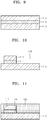
- FIGS. 9 to 15 illustrate a CMOS device manufacturing method according to another example embodiment.
- a buffer material layer 113 may be formed on a substrate 110, and a material layer 115 for an n-type transistor may be formed on the buffer material layer 113.
- the substrate 110 may be a silicon-based substrate.
- the substrate 110 may be doped with a p-type or n-type dopant.
- the substrate 110 may be a silicon substrate, and may be a p-type silicon substrate.
- the material layer 115 for the n-type transistor may be formed of a Group III-V material.
- the buffer material layer 113 may be formed of a Group III-V material of the same series as the material layer 115 for the n-type transistor. Since the buffer material layer 113 and the material layer 115 for the n-type transistor may be formed of the same materials and may perform the same operations as the buffer layer 13 and the material layer 15 of the n-type transistor described with reference to FIGS. 2 to 8 , detailed descriptions thereof will be omitted herein.
- the material layer 115 for the n-type transistor and the buffer material layer 113 may be etched to form a first layer 117 for the n-type transistor, a buffer layer 114 and a first pattern 118.
- the first pattern 118 may expose a portion of the substrate 110.
- an insulating layer 120 may be formed on the first layer 117 for the n-type transistor and an exposed region of the substrate 110.
- the insulating layer 120 may be formed of an oxide film, a nitride film, or an oxynitride film.
- the insulating layer 120 may be formed of a silicon oxide (SiO 2 ) film, a silicon nitride (SiN x ) film, or a silicon oxynitride (SiO x N y ) film.
- the insulating layer 120 may be etched to form a second pattern 123 for selective growth.
- the second pattern 123 may expose a portion of the substrate 110.
- a second layer 125 for a p-type transistor may be formed in the second pattern 123 by selective growth.
- the insulating layer 120 may be used as a mask in the selective growth process.
- the second layer 125 may be formed of a material including a Group IV material.
- the second layer 125 may be formed of germanium (Ge). Since the surface of the first layer 117 is covered with the insulating layer 120, the second layer 125 may be selectively grown on the exposed region of the substrate 110.
- the surfaces of the first layer 117 and the second layer 125 may be planarized through a planarization process. Accordingly, both the first layer 117 for the n-type transistor and the second layer 125 for the p-type transistor may be formed on one substrate 110. For example, selectively growing the second layer 125 formed of a single material may be easier and simpler than selectively growing the first layer 117 formed of a Group III-V compound material.
- a first source electrode S11 and a first drain electrode D11 may be formed at both sides of the first layer 117.
- the first source electrode S11 and the first drain electrode D11 may be formed at a top portion of the first layer 117 while being spaced apart from each other.
- a second source electrode S12 and a second drain electrode D12 may be formed at both sides of the second layer 125.
- a first spacer 133 may be formed on both sides of a first gate electrode G11.
- a second spacer 143 may be formed on both sides of a second gate electrode G12.
- the second source electrode S12 and the second drain electrode D12 may be formed at a top portion of the second layer 125 while being spaced apart from each other.
- a first gate insulating layer 130 may be formed on the first layer 117, and the first gate electrode G11 may be formed on the first gate insulating layer 130.
- a second gate insulating layer 140 may be formed on the second layer 125, and the second gate electrode G12 may be formed on the second gate insulating layer 140.
- a buffer layer 114 may be provided on a substrate 110, a first layer 117 for an n-type transistor may be provided on the buffer layer 114, and a second layer 125 for a p-type transistor may be provided on the substrate 110 while being spaced apart from the first layer 117. Also, an insulating layer 120 may be provided between the first layer 117 and the second layer 125.
- FIGS. 16 to 23 illustrate a CMOS device manufacturing method according to another example embodiment.
- a substrate 210 is prepared. Referring to FIG. 17 , the substrate 210 is etched to form a first pattern 212. Referring to FIG. 18 , a buffer layer 213 and a material layer 215 for an n-type transistor are formed in the first pattern 212. Referring to FIG. 19 , the material layer 215 for the n-type transistor is etched to form a first layer 217 for the n-type transistor and a second pattern 218. The second pattern 218 may be formed to expose the buffer layer 213 or to expose the substrate 210. FIG. 19 illustrates an example in which the buffer layer 213 is exposed.
- an insulating layer 220 is formed on the resulting structure illustrated in FIG. 19 .
- the insulating layer 220 may be etched to form a third pattern 223.
- the third pattern 223 may be a pattern for selective growth.
- a second layer 225 for a p-type transistor may be selectively grown in the third pattern 223.
- the insulating layer 220 may be used as a mask in the selective growth.
- the surfaces of the substrate 210, the first layer 217, and the second layer 225 may be planarized through a planarization process. Since the components using the same denotations as the components described with reference to FIGS. 2 and 8 may be formed of the same materials and may perform the same functions and operations as the corresponding components of FIGS. 2 and 8 , detailed description thereof will be omitted herein.
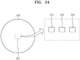
- FIG. 24 illustrates an example in which a first region 310, a second region 320, and a third region 330 are included in one cell 305 of a wafer 300.
- the first region 310 may be a silicon region 310
- the second region 320 may be a Group III-V compound region
- the third region 330 may be a Ge region.
- a photonic device may be provided in the first region 310
- an n-type transistor may be provided in the second region 320
- a p-type transistor may be provided in the third region 330.
- the photonic device may be a light emitting diode (LED), a laser diode (LD), or a photodiode (PD).
- the n-type transistor and the p-type transistor may operate as an electronic device that supports a light-emitting or light-receiving operation of the photonic device. Also, in this way, photonic device integration and hybrid electronic and photonic circuit integration may be possible.
Landscapes
- Metal-Oxide And Bipolar Metal-Oxide Semiconductor Integrated Circuits (AREA)
Claims (12)
- Procédé de fabrication d'un dispositif semi-conducteur à oxyde de métal complémentaire (CMOS) comprenant un substrat silicium (10), une couche tampon (13) sur le substrat silicium,
une première couche (17) pour un transistor de type n sur la couche tampon, une deuxième couche (25) pour un transistor de type p disposée sur la couche tampon (13) ou le substrat silicium (10) tout en étant espacée de la première couche (17) ; et une couche isolante (20) entre la première couche (17) et la deuxième couche (25), le procédé comprenant :la formation de la couche tampon (13) sur le substrat silicium (10) ; la formation d'une couche de matériau (15) pour un transistor de type n sur la couche tampon(13) ; la gravure de la couche de matériau (15) pour le transistor de type n pour former la première couche (17) pour le transistor de type n et d'un premier motif (18), dans lequel la première couche (17) est formée d'un matériau du groupe III-V ;le procédé caractérisé par : la formation de la couche isolante (20) sur la première couche (17) et du premier motif (18) ; la gravure de la couche isolante (20) pour former un deuxième motif (23) pour une croissance sélective ; etla croissance sélective de la deuxième couche (25) pour un transistor de type p dans le deuxième motif (23) dans lequel la deuxième couche (25) est formée d'un matériau du groupe IV. - Procédé selon la revendication 1, dans lequel la formation du premier motif inclut la gravure de la couche de matériau pour exposer une partie de la couche tampon.
- Procédé selon la revendication 1, dans lequel la formation du premier motif inclut la gravure de la couche de matériau pour exposer le substrat silicium.
- Procédé de fabrication d'un dispositif CMOS selon la revendication 1, 2 ou 3, dans lequel la couche tampon est formée d'un matériau du groupe III-V incluant au moins un élément parmi l'indium (In), le gallium (Ga) et l'aluminium (Al), et au moins un élément parmi l'arsenic (As), le phosphore (P) et l'antimoine (Sb).
- Procédé de fabrication d'un dispositif CMOS selon la revendication 4, dans lequel la couche tampon est formée d'au moins un élément parmi le InP, InAs, InSb, GaAs, GaP, GaSb, AIP, AlAs, AlSb, InAlAs, InGaP, GaAsP, InGaAsP et InGaAlAs.
- Procédé de fabrication d'un dispositif CMOS selon la revendication 4 ou 5, dans lequel la couche tampon est dopée avec un dopant de type n.
- Procédé de fabrication d'un dispositif CMOS selon la revendication 1, 2 ou 3, dans lequel la couche tampon comprend au moins un matériau du groupe IV.
- Procédé de fabrication d'un dispositif CMOS selon la revendication 7, dans lequel la couche tampon est formée d'au moins un élément parmi le SiGe, GeSn et germanium (Ge).
- Procédé de fabrication d'un dispositif CMOS selon l'une quelconque des revendications 1 à 8, dans lequel la première couche est formée d'au moins un élément parmi le InGaAs, InP, InSb, InGaSb, GaSb et InAs.
- Procédé de fabrication d'un dispositif CMOS selon la revendication 1, 2 ou 3, dans lequel la deuxième couche est formée de Ge.
- Procédé de fabrication d'un dispositif CMOS selon l'une quelconque des revendications 1 à 10, dans lequel le transistor de type n comprend un transistor à effet de champ à semi-conducteur à oxyde de métal (MOSFET) de type n et/ou le transistor de type p comprend un MOSFET de type p.
- Procédé de fabrication d'un dispositif CMOS selon l'une quelconque des revendications 1 à 11, dans lequel la première couche et la deuxième couche sont des couches de canaux.
Applications Claiming Priority (1)
| Application Number | Priority Date | Filing Date | Title |
|---|---|---|---|
| KR1020130107502A KR102210325B1 (ko) | 2013-09-06 | 2013-09-06 | Cmos 소자 및 그 제조 방법 |
Publications (3)
| Publication Number | Publication Date |
|---|---|
| EP2846353A2 EP2846353A2 (fr) | 2015-03-11 |
| EP2846353A3 EP2846353A3 (fr) | 2015-08-12 |
| EP2846353B1 true EP2846353B1 (fr) | 2017-11-01 |
Family
ID=51453694
Family Applications (1)
| Application Number | Title | Priority Date | Filing Date |
|---|---|---|---|
| EP14183431.7A Active EP2846353B1 (fr) | 2013-09-06 | 2014-09-03 | Procédé de fabrication d'un dispositif à semi-conducteur à oxyde de métal complémentaire |
Country Status (4)
| Country | Link |
|---|---|
| US (1) | US9425104B2 (fr) |
| EP (1) | EP2846353B1 (fr) |
| KR (1) | KR102210325B1 (fr) |
| CN (1) | CN104425492B (fr) |
Families Citing this family (8)
| Publication number | Priority date | Publication date | Assignee | Title |
|---|---|---|---|---|
| US8941118B1 (en) * | 2011-07-29 | 2015-01-27 | Hrl Laboratories, Llc | Normally-off III-nitride transistors with high threshold-voltage and low on-resistance |
| KR102104062B1 (ko) * | 2013-10-31 | 2020-04-23 | 삼성전자 주식회사 | 기판 구조체, 이를 포함한 cmos 소자 및 cmos 소자 제조 방법 |
| US11025029B2 (en) | 2015-07-09 | 2021-06-01 | International Business Machines Corporation | Monolithic III-V nanolaser on silicon with blanket growth |
| US10153300B2 (en) * | 2016-02-05 | 2018-12-11 | Taiwan Semiconductor Manufacturing Company Limited | Semiconductor device including a high-electron-mobility transistor (HEMT) and method for manufacturing the same |
| US11222982B2 (en) * | 2016-09-29 | 2022-01-11 | Intel Corporation | Methods and apparatus to form silicon-based transistors on group III-nitride materials using aspect ratio trapping |
| KR102034175B1 (ko) | 2017-05-30 | 2019-10-18 | 한국과학기술연구원 | 수평 배열된 반도체 채널을 가지는 반도체 소자 및 이의 제조 방법 |
| KR102549586B1 (ko) * | 2017-08-17 | 2023-07-03 | 한국전자통신연구원 | 융합 반도체 장치 및 그 제조 방법 |
| KR102722449B1 (ko) * | 2022-10-07 | 2024-10-24 | 연세대학교 산학협력단 | 다중 파장 이미지 저장 소자 및 이의 제조 방법 |
Family Cites Families (25)
| Publication number | Priority date | Publication date | Assignee | Title |
|---|---|---|---|---|
| US6563143B2 (en) * | 1999-07-29 | 2003-05-13 | Stmicroelectronics, Inc. | CMOS circuit of GaAs/Ge on Si substrate |
| US20040012037A1 (en) | 2002-07-18 | 2004-01-22 | Motorola, Inc. | Hetero-integration of semiconductor materials on silicon |
| US7153753B2 (en) * | 2003-08-05 | 2006-12-26 | Micron Technology, Inc. | Strained Si/SiGe/SOI islands and processes of making same |
| US7138697B2 (en) | 2004-02-24 | 2006-11-21 | International Business Machines Corporation | Structure for and method of fabricating a high-speed CMOS-compatible Ge-on-insulator photodetector |
| JP4177775B2 (ja) * | 2004-03-16 | 2008-11-05 | 株式会社東芝 | 半導体基板及びその製造方法並びに半導体装置 |
| US7422956B2 (en) | 2004-12-08 | 2008-09-09 | Advanced Micro Devices, Inc. | Semiconductor device and method of making semiconductor device comprising multiple stacked hybrid orientation layers |
| US7569873B2 (en) | 2005-10-28 | 2009-08-04 | Dsm Solutions, Inc. | Integrated circuit using complementary junction field effect transistor and MOS transistor in silicon and silicon alloys |
| KR100843229B1 (ko) | 2007-01-11 | 2008-07-02 | 삼성전자주식회사 | 하이브리드 구조의 전하 트랩막을 포함하는 플래쉬 메모리소자 및 그 제조 방법 |
| US7510940B2 (en) | 2007-02-16 | 2009-03-31 | Taiwan Semiconductor Manufacturing Company, Ltd. | Method for fabricating dual-gate semiconductor device |
| US9006707B2 (en) * | 2007-02-28 | 2015-04-14 | Intel Corporation | Forming arsenide-based complementary logic on a single substrate |
| KR20090038653A (ko) | 2007-10-16 | 2009-04-21 | 삼성전자주식회사 | Cmos 소자 및 그 제조방법 |
| KR101020841B1 (ko) | 2008-03-31 | 2011-03-09 | 고려대학교 산학협력단 | 씨모스 장치 및 이의 제조방법 |
| CN102113114B (zh) | 2008-07-25 | 2013-08-28 | 国立大学法人东北大学 | 互补型逻辑门器件 |
| KR20100078548A (ko) | 2008-12-30 | 2010-07-08 | 주식회사 동부하이텍 | 듀얼 게이트를 갖는 씨모스 반도체 소자의 제조방법 |
| US8530938B2 (en) * | 2009-12-10 | 2013-09-10 | International Rectifier Corporation | Monolithic integrated composite group III-V and group IV semiconductor device and method for fabricating same |
| US8212294B2 (en) | 2010-01-28 | 2012-07-03 | Raytheon Company | Structure having silicon CMOS transistors with column III-V transistors on a common substrate |
| CN102790084B (zh) * | 2011-05-16 | 2016-03-16 | 中国科学院上海微系统与信息技术研究所 | 锗和iii-v混合共平面的soi半导体结构及其制备方法 |
| CN102790054B (zh) * | 2011-05-16 | 2015-09-16 | 中国科学院上海微系统与信息技术研究所 | 锗和iii-v混合共平面的半导体结构及其制备方法 |
| CN102842595B (zh) * | 2011-06-20 | 2015-12-02 | 中国科学院微电子研究所 | 半导体器件及其制造方法 |
| US9165835B2 (en) | 2011-08-30 | 2015-10-20 | Taiwan Semiconductor Manufacturing Co., Ltd. | Method and structure for advanced semiconductor channel substrate materials |
| US20130137238A1 (en) | 2011-11-30 | 2013-05-30 | Taiwan Semiconductor Manufacturing Company, Ltd. | Method for forming high mobility channels in iii-v family channel devices |
| US8471342B1 (en) * | 2011-12-09 | 2013-06-25 | GlobalFoundries, Inc. | Integrated circuits formed on strained substrates and including relaxed buffer layers and methods for the manufacture thereof |
| KR101167530B1 (ko) | 2012-01-05 | 2012-07-20 | 주식회사 시지트로닉스 | 수퍼 헤테로 접합 반도체소자 및 그 제작방법 |
| CN103258796B (zh) * | 2013-05-14 | 2015-01-28 | 中国科学院半导体研究所 | 硅基高迁移率沟道cmos的制备方法 |
| CN103390591B (zh) | 2013-07-22 | 2015-11-25 | 中国科学院半导体研究所 | 硅基高迁移率Ⅲ-V/Ge沟道的CMOS制备方法 |
-
2013
- 2013-09-06 KR KR1020130107502A patent/KR102210325B1/ko active Active
-
2014
- 2014-04-23 US US14/259,569 patent/US9425104B2/en active Active
- 2014-09-02 CN CN201410442976.4A patent/CN104425492B/zh active Active
- 2014-09-03 EP EP14183431.7A patent/EP2846353B1/fr active Active
Non-Patent Citations (1)
| Title |
|---|
| None * |
Also Published As
| Publication number | Publication date |
|---|---|
| CN104425492A (zh) | 2015-03-18 |
| KR102210325B1 (ko) | 2021-02-01 |
| US9425104B2 (en) | 2016-08-23 |
| EP2846353A2 (fr) | 2015-03-11 |
| KR20150028626A (ko) | 2015-03-16 |
| US20150069517A1 (en) | 2015-03-12 |
| CN104425492B (zh) | 2019-03-22 |
| EP2846353A3 (fr) | 2015-08-12 |
Similar Documents
| Publication | Publication Date | Title |
|---|---|---|
| EP2846353B1 (fr) | Procédé de fabrication d'un dispositif à semi-conducteur à oxyde de métal complémentaire | |
| KR102551812B1 (ko) | 가공된 기판과 통합된 전자 전력 디바이스 | |
| KR102681469B1 (ko) | 가공된 기판 상의 집적된 디바이스를 위한 시스템 및 방법 | |
| US9412911B2 (en) | Optical tuning of light emitting semiconductor junctions | |
| US9312377B2 (en) | Semiconductor devices and methods of manufacturing the same | |
| EP2787525A1 (fr) | Structures de substrat et dispositifs semi-conducteurs l'employant | |
| US8866154B2 (en) | Lattice mismatched heterojunction structures and devices made therefrom | |
| US9105496B2 (en) | Complementary metal oxide semiconductor device, optical apparatus including the same, and method of manufacturing the same | |
| JP6525554B2 (ja) | 基板構造体を含むcmos素子 | |
| US20110315953A1 (en) | Method of forming compound semiconductor | |
| US9595616B1 (en) | Vertical III-nitride thin-film power diode | |
| US8536028B1 (en) | Self alignment and assembly fabrication method for stacking multiple material layers | |
| KR102034175B1 (ko) | 수평 배열된 반도체 채널을 가지는 반도체 소자 및 이의 제조 방법 | |
| JP2014090122A (ja) | 複合基板の製造方法 | |
| Liu et al. | n+ Si/pGe Heterojunctions Fabricated by Narrow Membrane Bonding |
Legal Events
| Date | Code | Title | Description |
|---|---|---|---|
| 17P | Request for examination filed |
Effective date: 20140903 |
|
| AK | Designated contracting states |
Kind code of ref document: A2 Designated state(s): AL AT BE BG CH CY CZ DE DK EE ES FI FR GB GR HR HU IE IS IT LI LT LU LV MC MK MT NL NO PL PT RO RS SE SI SK SM TR |
|
| AX | Request for extension of the european patent |
Extension state: BA ME |
|
| PUAI | Public reference made under article 153(3) epc to a published international application that has entered the european phase |
Free format text: ORIGINAL CODE: 0009012 |
|
| PUAL | Search report despatched |
Free format text: ORIGINAL CODE: 0009013 |
|
| AK | Designated contracting states |
Kind code of ref document: A3 Designated state(s): AL AT BE BG CH CY CZ DE DK EE ES FI FR GB GR HR HU IE IS IT LI LT LU LV MC MK MT NL NO PL PT RO RS SE SI SK SM TR |
|
| AX | Request for extension of the european patent |
Extension state: BA ME |
|
| RIC1 | Information provided on ipc code assigned before grant |
Ipc: H01L 27/06 20060101ALI20150706BHEP Ipc: H01L 27/092 20060101ALI20150706BHEP Ipc: H01L 21/8238 20060101ALI20150706BHEP Ipc: H01L 21/8252 20060101AFI20150706BHEP Ipc: H01L 21/8258 20060101ALI20150706BHEP |
|
| R17P | Request for examination filed (corrected) |
Effective date: 20160212 |
|
| RBV | Designated contracting states (corrected) |
Designated state(s): AL AT BE BG CH CY CZ DE DK EE ES FI FR GB GR HR HU IE IS IT LI LT LU LV MC MK MT NL NO PL PT RO RS SE SI SK SM TR |
|
| GRAP | Despatch of communication of intention to grant a patent |
Free format text: ORIGINAL CODE: EPIDOSNIGR1 |
|
| INTG | Intention to grant announced |
Effective date: 20170601 |
|
| GRAS | Grant fee paid |
Free format text: ORIGINAL CODE: EPIDOSNIGR3 |
|
| GRAA | (expected) grant |
Free format text: ORIGINAL CODE: 0009210 |
|
| AK | Designated contracting states |
Kind code of ref document: B1 Designated state(s): AL AT BE BG CH CY CZ DE DK EE ES FI FR GB GR HR HU IE IS IT LI LT LU LV MC MK MT NL NO PL PT RO RS SE SI SK SM TR |
|
| REG | Reference to a national code |
Ref country code: GB Ref legal event code: FG4D |
|
| REG | Reference to a national code |
Ref country code: CH Ref legal event code: EP Ref country code: AT Ref legal event code: REF Ref document number: 942823 Country of ref document: AT Kind code of ref document: T Effective date: 20171115 |
|
| REG | Reference to a national code |
Ref country code: IE Ref legal event code: FG4D |
|
| REG | Reference to a national code |
Ref country code: DE Ref legal event code: R096 Ref document number: 602014016493 Country of ref document: DE |
|
| REG | Reference to a national code |
Ref country code: NL Ref legal event code: MP Effective date: 20171101 |
|
| REG | Reference to a national code |
Ref country code: LT Ref legal event code: MG4D |
|
| REG | Reference to a national code |
Ref country code: AT Ref legal event code: MK05 Ref document number: 942823 Country of ref document: AT Kind code of ref document: T Effective date: 20171101 |
|
| PG25 | Lapsed in a contracting state [announced via postgrant information from national office to epo] |
Ref country code: NL Free format text: LAPSE BECAUSE OF FAILURE TO SUBMIT A TRANSLATION OF THE DESCRIPTION OR TO PAY THE FEE WITHIN THE PRESCRIBED TIME-LIMIT Effective date: 20171101 Ref country code: FI Free format text: LAPSE BECAUSE OF FAILURE TO SUBMIT A TRANSLATION OF THE DESCRIPTION OR TO PAY THE FEE WITHIN THE PRESCRIBED TIME-LIMIT Effective date: 20171101 Ref country code: LT Free format text: LAPSE BECAUSE OF FAILURE TO SUBMIT A TRANSLATION OF THE DESCRIPTION OR TO PAY THE FEE WITHIN THE PRESCRIBED TIME-LIMIT Effective date: 20171101 Ref country code: SE Free format text: LAPSE BECAUSE OF FAILURE TO SUBMIT A TRANSLATION OF THE DESCRIPTION OR TO PAY THE FEE WITHIN THE PRESCRIBED TIME-LIMIT Effective date: 20171101 Ref country code: NO Free format text: LAPSE BECAUSE OF FAILURE TO SUBMIT A TRANSLATION OF THE DESCRIPTION OR TO PAY THE FEE WITHIN THE PRESCRIBED TIME-LIMIT Effective date: 20180201 Ref country code: ES Free format text: LAPSE BECAUSE OF FAILURE TO SUBMIT A TRANSLATION OF THE DESCRIPTION OR TO PAY THE FEE WITHIN THE PRESCRIBED TIME-LIMIT Effective date: 20171101 |
|
| PG25 | Lapsed in a contracting state [announced via postgrant information from national office to epo] |
Ref country code: AT Free format text: LAPSE BECAUSE OF FAILURE TO SUBMIT A TRANSLATION OF THE DESCRIPTION OR TO PAY THE FEE WITHIN THE PRESCRIBED TIME-LIMIT Effective date: 20171101 Ref country code: HR Free format text: LAPSE BECAUSE OF FAILURE TO SUBMIT A TRANSLATION OF THE DESCRIPTION OR TO PAY THE FEE WITHIN THE PRESCRIBED TIME-LIMIT Effective date: 20171101 Ref country code: BG Free format text: LAPSE BECAUSE OF FAILURE TO SUBMIT A TRANSLATION OF THE DESCRIPTION OR TO PAY THE FEE WITHIN THE PRESCRIBED TIME-LIMIT Effective date: 20180201 Ref country code: LV Free format text: LAPSE BECAUSE OF FAILURE TO SUBMIT A TRANSLATION OF THE DESCRIPTION OR TO PAY THE FEE WITHIN THE PRESCRIBED TIME-LIMIT Effective date: 20171101 Ref country code: RS Free format text: LAPSE BECAUSE OF FAILURE TO SUBMIT A TRANSLATION OF THE DESCRIPTION OR TO PAY THE FEE WITHIN THE PRESCRIBED TIME-LIMIT Effective date: 20171101 Ref country code: GR Free format text: LAPSE BECAUSE OF FAILURE TO SUBMIT A TRANSLATION OF THE DESCRIPTION OR TO PAY THE FEE WITHIN THE PRESCRIBED TIME-LIMIT Effective date: 20180202 Ref country code: IS Free format text: LAPSE BECAUSE OF FAILURE TO SUBMIT A TRANSLATION OF THE DESCRIPTION OR TO PAY THE FEE WITHIN THE PRESCRIBED TIME-LIMIT Effective date: 20180301 |
|
| PG25 | Lapsed in a contracting state [announced via postgrant information from national office to epo] |
Ref country code: SK Free format text: LAPSE BECAUSE OF FAILURE TO SUBMIT A TRANSLATION OF THE DESCRIPTION OR TO PAY THE FEE WITHIN THE PRESCRIBED TIME-LIMIT Effective date: 20171101 Ref country code: DK Free format text: LAPSE BECAUSE OF FAILURE TO SUBMIT A TRANSLATION OF THE DESCRIPTION OR TO PAY THE FEE WITHIN THE PRESCRIBED TIME-LIMIT Effective date: 20171101 Ref country code: CY Free format text: LAPSE BECAUSE OF FAILURE TO SUBMIT A TRANSLATION OF THE DESCRIPTION OR TO PAY THE FEE WITHIN THE PRESCRIBED TIME-LIMIT Effective date: 20171101 Ref country code: EE Free format text: LAPSE BECAUSE OF FAILURE TO SUBMIT A TRANSLATION OF THE DESCRIPTION OR TO PAY THE FEE WITHIN THE PRESCRIBED TIME-LIMIT Effective date: 20171101 Ref country code: CZ Free format text: LAPSE BECAUSE OF FAILURE TO SUBMIT A TRANSLATION OF THE DESCRIPTION OR TO PAY THE FEE WITHIN THE PRESCRIBED TIME-LIMIT Effective date: 20171101 |
|
| REG | Reference to a national code |
Ref country code: DE Ref legal event code: R097 Ref document number: 602014016493 Country of ref document: DE |
|
| PG25 | Lapsed in a contracting state [announced via postgrant information from national office to epo] |
Ref country code: RO Free format text: LAPSE BECAUSE OF FAILURE TO SUBMIT A TRANSLATION OF THE DESCRIPTION OR TO PAY THE FEE WITHIN THE PRESCRIBED TIME-LIMIT Effective date: 20171101 Ref country code: IT Free format text: LAPSE BECAUSE OF FAILURE TO SUBMIT A TRANSLATION OF THE DESCRIPTION OR TO PAY THE FEE WITHIN THE PRESCRIBED TIME-LIMIT Effective date: 20171101 Ref country code: SM Free format text: LAPSE BECAUSE OF FAILURE TO SUBMIT A TRANSLATION OF THE DESCRIPTION OR TO PAY THE FEE WITHIN THE PRESCRIBED TIME-LIMIT Effective date: 20171101 Ref country code: PL Free format text: LAPSE BECAUSE OF FAILURE TO SUBMIT A TRANSLATION OF THE DESCRIPTION OR TO PAY THE FEE WITHIN THE PRESCRIBED TIME-LIMIT Effective date: 20171101 |
|
| PLBE | No opposition filed within time limit |
Free format text: ORIGINAL CODE: 0009261 |
|
| STAA | Information on the status of an ep patent application or granted ep patent |
Free format text: STATUS: NO OPPOSITION FILED WITHIN TIME LIMIT |
|
| 26N | No opposition filed |
Effective date: 20180802 |
|
| PG25 | Lapsed in a contracting state [announced via postgrant information from national office to epo] |
Ref country code: SI Free format text: LAPSE BECAUSE OF FAILURE TO SUBMIT A TRANSLATION OF THE DESCRIPTION OR TO PAY THE FEE WITHIN THE PRESCRIBED TIME-LIMIT Effective date: 20171101 |
|
| PG25 | Lapsed in a contracting state [announced via postgrant information from national office to epo] |
Ref country code: MC Free format text: LAPSE BECAUSE OF FAILURE TO SUBMIT A TRANSLATION OF THE DESCRIPTION OR TO PAY THE FEE WITHIN THE PRESCRIBED TIME-LIMIT Effective date: 20171101 |
|
| REG | Reference to a national code |
Ref country code: CH Ref legal event code: PL |
|
| GBPC | Gb: european patent ceased through non-payment of renewal fee |
Effective date: 20180903 |
|
| REG | Reference to a national code |
Ref country code: BE Ref legal event code: MM Effective date: 20180930 |
|
| REG | Reference to a national code |
Ref country code: IE Ref legal event code: MM4A |
|
| PG25 | Lapsed in a contracting state [announced via postgrant information from national office to epo] |
Ref country code: LU Free format text: LAPSE BECAUSE OF NON-PAYMENT OF DUE FEES Effective date: 20180903 |
|
| PG25 | Lapsed in a contracting state [announced via postgrant information from national office to epo] |
Ref country code: IE Free format text: LAPSE BECAUSE OF NON-PAYMENT OF DUE FEES Effective date: 20180903 |
|
| PG25 | Lapsed in a contracting state [announced via postgrant information from national office to epo] |
Ref country code: BE Free format text: LAPSE BECAUSE OF NON-PAYMENT OF DUE FEES Effective date: 20180930 Ref country code: CH Free format text: LAPSE BECAUSE OF NON-PAYMENT OF DUE FEES Effective date: 20180930 Ref country code: LI Free format text: LAPSE BECAUSE OF NON-PAYMENT OF DUE FEES Effective date: 20180930 Ref country code: FR Free format text: LAPSE BECAUSE OF NON-PAYMENT OF DUE FEES Effective date: 20180930 |
|
| PG25 | Lapsed in a contracting state [announced via postgrant information from national office to epo] |
Ref country code: GB Free format text: LAPSE BECAUSE OF NON-PAYMENT OF DUE FEES Effective date: 20180903 |
|
| PG25 | Lapsed in a contracting state [announced via postgrant information from national office to epo] |
Ref country code: MT Free format text: LAPSE BECAUSE OF NON-PAYMENT OF DUE FEES Effective date: 20180903 |
|
| PG25 | Lapsed in a contracting state [announced via postgrant information from national office to epo] |
Ref country code: TR Free format text: LAPSE BECAUSE OF FAILURE TO SUBMIT A TRANSLATION OF THE DESCRIPTION OR TO PAY THE FEE WITHIN THE PRESCRIBED TIME-LIMIT Effective date: 20171101 |
|
| PG25 | Lapsed in a contracting state [announced via postgrant information from national office to epo] |
Ref country code: HU Free format text: LAPSE BECAUSE OF FAILURE TO SUBMIT A TRANSLATION OF THE DESCRIPTION OR TO PAY THE FEE WITHIN THE PRESCRIBED TIME-LIMIT; INVALID AB INITIO Effective date: 20140903 Ref country code: PT Free format text: LAPSE BECAUSE OF FAILURE TO SUBMIT A TRANSLATION OF THE DESCRIPTION OR TO PAY THE FEE WITHIN THE PRESCRIBED TIME-LIMIT Effective date: 20171101 |
|
| PG25 | Lapsed in a contracting state [announced via postgrant information from national office to epo] |
Ref country code: MK Free format text: LAPSE BECAUSE OF NON-PAYMENT OF DUE FEES Effective date: 20171101 |
|
| PG25 | Lapsed in a contracting state [announced via postgrant information from national office to epo] |
Ref country code: AL Free format text: LAPSE BECAUSE OF FAILURE TO SUBMIT A TRANSLATION OF THE DESCRIPTION OR TO PAY THE FEE WITHIN THE PRESCRIBED TIME-LIMIT Effective date: 20171101 |
|
| P01 | Opt-out of the competence of the unified patent court (upc) registered |
Effective date: 20230520 |
|
| REG | Reference to a national code |
Ref country code: DE Ref legal event code: R079 Ref document number: 602014016493 Country of ref document: DE Free format text: PREVIOUS MAIN CLASS: H01L0021825200 Ipc: H10D0084050000 |
|
| PGFP | Annual fee paid to national office [announced via postgrant information from national office to epo] |
Ref country code: DE Payment date: 20250722 Year of fee payment: 12 |